LME49811TB中文资料
LME49810运用
随着输出的电平增加,被提取进入“Zobel”网络的电流也随之会上升。因此,在任 何条件下输出网络中元件的额定参数都必须足够。
3. 可减轻交流耦合 RC 网络的噪声。
负反馈系数 功率放大器的负反馈设置可为系统带来较高的稳定性和线性度。采用负反馈可防止 放大器直流偏移电压出现饱和。一般来说,当放大器在高频工作时会出现相位位 移,而较大的负反馈系数可减轻在高频时的不稳定性和振荡。
在离散的放大器系统中,高反馈系数将会引起很差的瞬态响应或高频不稳定性。然 而,LME49810 拥有一个较高的开环增益,因此它的闭环增益误差和电源纹波抑制 会较小,可以最大化电路中的负反馈,从而提高系统的线性度。通常,建议采用 30dB 至 40dB 的电压增益。 通过设置输入电阻和反馈电阻,很容易就可以设定出负反馈系数
静音控制、静音 输出偏置及输出级 输出偏置电路
LME49810 有两根用来设定偏置的专用引脚(BIASP 和 BIASM),可以提供一定的输 出偏置电流。可变电阻器 R pot 可用来调节输出级的偏置电流,将 R pot+Rb1 的电 阻降低可以提高偏置电压。 倍增器 QMULT 用来补偿偏置电压以防止双极输出晶 体管出现热漂移。 QMULT 必须与输出晶体管连接在相同的散热器上。当温度上升时,Vbe 会减小以 降低偏置电压,较高的偏置电流可减少输出的交越失真,但同时会消耗较大的电 流。
等效RE Amp
RE
Rload
此外,RE电阻是开环输出阻抗的主要成份。闭环输出阻抗由开环输出阻抗和负反 馈系数来定义,其关系如下:
JUMO设备型号说明书
Page 2/2
Accessories for Programmers, Thermostats, Microstats and Controllers
Device designation
DICON 400/500 DICON 401/501
Data Sheet 70.3570 Data Sheet 70.3580
Software programs1 (multilingual)
x
Setup program, program editor and Startup
x
Setup program
x
Setup program
x
Setup program
x
Program editor
x
Setup program and program editor
e-mail:
mail@
Internet:
JUMO Instrument Co. Ltd. JUMO House Temple Bank, Riverway Harlow, Essex CM 20 2TT, UK Phone: +44 1279 635533 Fax: +44 1279 635262 e-mail: sales@ Internet:
eTRON T eTRON M
Data Sheet 70.1050 Data Sheet 70.1060
eTRON M100
Data Sheet 70.1061
iTRON 04 B
Data Sheet 70.2050
mTRON
Data Sheet 70.4010 ... 45
LME49600中文资料
±550
±1.0
±2.5
±3.0
±5.0
7.5 5.5
±17
±60
±100
Units (Limits)
V (min) V (min) V (min)
V (min) V (min) V (min)
mA mA (max) mA (max)
μA (max) μA (max)
MΩ MΩ mV (max) μV/°C
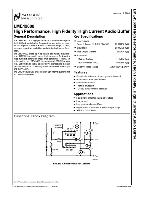
Functional Block Diagram
30029805
FIGURE 1. Functional Block Diagram
Boomer® is a registered trademark of National Semiconductor Corporation.
1150 型号说明书

Thermo Fisher Scientific Air Quality Instruments 27 Forge Parkway Franklin, MA 02038 1-508-520-0430 /aqi
WEEE iance
This product is required to comply with the European Union’s Waste Electrical & Electronic Equipment (WEEE) Directive 2002/96/EC. It is marked with the following symbol:
用LME49810制作高性能功率放大器

⽤LME49810制作⾼性能功率放⼤器距离第⼀篇⽂章发表已有好长⼀段时间了(因⼥⼉出⽣),现在我的⼩⼥⼉已经1岁多,所以我的制作和研究⼜可以继续了。
在第⼀篇⽂章中,曾推荐了⼀款采⽤国半⾼性能驱动芯⽚LME49810的功放。
这块芯⽚的性能已经在不同负载下测量过。
得出的建议是,驱动级必须要为输出级提供⾜够的驱动电流,输出级由此选择 ON(安森美)的NJL3281D/1302D。
这对管⼦由于内含偏置⼆极管,具有同时实现热补偿功能,因此传统的Vbe倍乘器就可以取消了。
在本⽂中主要介绍电源部分的设计及如何借助仪器监测功放的THD(总谐波失真加噪声)指标、如何⽤频谱分析的⽅法来调整功放的静态电流⾄最佳值,最后部分是功放的性能测试结果,其中包括了THD测试、IMD测试和⽅波测试。
⼀、电源设计本功放设计在8Ω负载上⾄少有120W输出。
这样,每个输出级晶体管将分担1.9A的有效值电流(本功放使⽤了两对管⼦)。
从NJL3281D/1302D的资料可知,其V ce的线性⼯作区的最⼩值是5V,这样要满⾜满功率输出,电源电压(V+、V-)⾄少要达到49V,其计算如下:P out=120(W)=I 2out×8=V 2out /8Iout= 120/8= 15≈3.87(A)V +=V - = 120×8× 2+5≈49(V)电源部分电路如图1所⽰。
V+ 及V-在满功率输出状态起码要49V,加上变压器的损耗和纹波,我们选择了未经稳压的±55V,此时变压器次级电压为交流39V。
桥堆中的⼆极管在⼤电流状态下会有约1V的压降,同时我们也必须考虑市电电压的变化,这样,就需要⼀个双0~42V次级电压绕组的变压器,且次级必须要能提供4A的有效值电流。
如果你希望在4Ω负载上得到翻倍的输出功率,就必须要有⼀个满⾜8A电流的变压器!光有⼤变压器还不⾏,⼤⽔塘式电容也是必要的。
我使⽤了两个桥堆(B1、B2)来组成双桥全波整流,这样DC 0V 也包含在整流回路中。
LME49740中文资料

February 2007LME49740Quad High Performance, High Fidelity Audio Operational AmplifierGeneral DescriptionThe LME49740 is part of the ultra-low distortion, low noise,high slew rate operational amplifier series optimized and fully specified for high performance, high fidelity bining advanced leading-edge process technology with state-of-the-art circuit design, the LME49740 audio opera-tional amplifiers deliver superior audio signal amplification for outstanding audio performance. The LME49740 combines extremely low voltage noise density (2.7nV/√HZ) with van-ishingly low TH D+N (0.00003%) to easily satisfy the most demanding audio applications. To ensure that the most chal-lenging loads are driven without compromise, the LME49740has a high slew rate of ±20V/μs and an output current capa-bility of ±26mA. Further, dynamic range is maximized by an output stage that drives 2k Ω loads to within 1V of either power supply voltage and to within 1.4V when driving 600Ω loads.The LME49740's outstanding CMRR(120dB), PSRR(120dB),and V OS (0.1mV) give the amplifier excellent operational am-plifier DC performance.The LME49740 has a wide supply range of ±2.5V to ±17V.Over this supply range the LME49740’s input circuitry main-tains excellent common-mode and power supply rejection, as well as maintaining its low input bias current. The LME49740is unity gain stable. The Audio Operational Amplifier achieves outstanding AC performance while driving complex loads with values as high as 100pF.The LME49740 is available in 14–lead narrow body SOIC and 14–lead plastic DIP. Demonstration boards are available for each package.Key Specifications■ Power Supply Voltage Range ±2.5V to ±17V■ THD+N (A V = 1, V OUT = 3V RMS , f IN = 1kHz)R L = 2k Ω0.00003% (typ) R L = 600Ω0.00003% (typ)■ Input Noise Density 2.7nV/√Hz (typ)■ Slew Rate±20V/μs (typ)■ Gain Bandwidth Product 55MHz (typ)■ Open Loop Gain (R L = 600Ω)140dB (typ)■ Input Bias Current 10nA (typ)■ Input Offset Voltage 0.1mV (typ)■ DC Gain Linearity Error0.000009%Features■Easily drives 600Ω loads■Optimized for superior audio signal fidelity ■Output short circuit protection■PSRR and CMRR exceed 120dB (typ)■SOIC and DIP packagesApplications■Ultra high quality audio amplification ■High fidelity preamplifiers ■High fidelity multimedia■State of the art phono pre amps■High performance professional audio■High fidelity equalization and crossover networks ■High performance line drivers ■High performance line receivers ■High fidelity active filters© 2007 National Semiconductor Corporation LME49740 Quad High Performance, High Fidelity Audio Operational AmplifierTypical Application20210502FIGURE 1. Passively Equalized RIAA Phono PreamplifierConnection Diagram20210501Order Number LME49740MA See NS Package Number — M14A Order Number LME49740NA See NS Package Number — N14A 2L M E 49740Absolute Maximum Ratings (Notes 1, 2)If Military/Aerospace specified devices are required,please contact the National Semiconductor Sales Office/Distributors for availability and specifications.Power Supply Voltage (V S = V + - V -)36VStorage Temperature −65°C to 150°CInput Voltage(V-) - 0.7V to (V+) + 0.7VOutput Short Circuit (Note 3)Continuous Power DissipationInternally LimitedESD Susceptibility (Note 4)2000V ESD Susceptibility (Note 5)200V Junction Temperature 150°CThermal Resistance θJA (MA)107°C/W θJA (NA)74°C/WTemperature RangeT MIN ≤ T A ≤ T MAX –40°C ≤ T A ≤ 85°C Supply Voltage Range±2.5V ≤ V S ≤ ± 17VElectrical Characteristics(Notes 1, 2)The following specifications apply for V S = ±15V, R L = 2k Ω, f IN = 1kHz,and T A = 25C, unless otherwise specified.SymbolParameterConditionsLME49740Units (Limits)Typical Limit (Note 6)(Notes 7, 8)THD+NTotal Harmonic Distortion + NoiseA V = 1, V OUT = 3V RMSR L = 2k Ω R L = 600Ω0.000030.000030.00009% (max)% (max)IMD Intermodulation Distortion A V = 1, V OUT = 3V RMSTwo-tone, 60Hz & 7kHz 4:10.00005 % (max)GBWP Gain Bandwidth Product 5545MHz (min)SR Slew Rate±20±15V/μs (min)FPBWFull Power BandwidthV OUT = 1V P-P , –3dBreferenced to output magnitude at f = 1kHz10MHzt sSettling timeA V = 1, 10V step, C L = 100pF 0.1% error range 1.2μs e nEquivalent Input Noise Voltagef BW = 20Hz to 20kHz 0.340.65μV RMSEquivalent Input Noise Density f = 1kHz f = 10Hz 2.76.4 4.7 nV /√Hz nV /√Hz i n Current Noise Density f = 1kHz f = 10Hz 1.63.1 pA /√Hz pA /√HzV OSOffset Voltage±0.1±0.7mV (max)ΔV OS /ΔTemp Average Input Offset Voltage Drift vsTemperature40°C ≤ T A ≤ 85°C0.2 μV/°C PSRR Average Input Offset Voltage Shift vsPower Supply Voltage ΔV S = 20V (Note 9)120110dB (min)ISO CH-CH Channel-to-Channel Isolation f IN = 1kHz f IN = 20kHz 118112 dB dB I BInput Bias Current V CM = 0V1072nA (max)ΔI OS /ΔTemp Input Bias Current Drift vs Temperature –40°C ≤ T A ≤ 85°C 0.1 nA/°C I OS Input Offset CurrentV CM = 0V1165nA (max)V IN-CM Common-Mode Input Voltage Range +14.1–13.9(V+)–2.0(V-)+2.0V (min)V (min)CMRR Common-Mode Rejection –10V<V CM <10V 120110dB (min)Z INDifferential Input Impedance30 k ΩCommon Mode Input Impedance –10V<V CM <10V1000 M ΩA VOLOpen Loop Voltage Gain–10V<V OUT <10V, R L = 600Ω140 dB (min)–10V<V OUT <10V, R L = 2k Ω140 dB (min)–10V<V OUT <10V, R L = 10k Ω140125dB (min)3LME49740SymbolParameterConditionsLME49740Units (Limits)Typical Limit (Note 6)(Notes 7, 8)V OUTMAX Maximum Output Voltage Swing R L = 600Ω±13.6±12.5V (min)R L = 2k Ω±14.0 V (min)R L = 10k Ω±14.1 V (min)I OUT Output Current R L = 600Ω, V S = ±17V ±26±23mA (min)I OUT-CC Short Circuit Current+30–38 mA mAR OUT Output Impedancef IN = 10kHz Closed-Loop Open-Loop 0.0113ΩΩC LOAD Capacitive Load Drive Overshoot 100pF 16 %I STotal Quiescent CurrentI OUT = 0mA18.520mA (max)Note 1:Absolute Maximum Ratings indicate limits beyond which damage to the device may occur.Note 2:Operating Ratings indicate conditions for which the device is functional, but do not guarantee specific performance limits. For guaranteed specifications and test conditions, see the Electrical Characteristics. The guaranteed specifications apply only for the test conditions listed. Some performance characteristics may degrade when the device is not operated under the listed test conditions.Note 3:Amplifier output connected to GND, any number of amplifiers within a package.Note 4:Human body model, 100pF discharged through a 1.5k Ω resistor.Note 5:Machine Model ESD test is covered by specification EIAJ IC-121-1981. A 200pF cap is charged to the specified voltage and then discharged directly into the IC with no external series resistor (resistance of discharge path must be under 50Ω).Note 6:Typical specifications are specified at +25ºC and represent the most likely parametric norm.Note 7:Tested limits are guaranteed to National's AOQL (Average Outgoing Quality Level).Note 8:Datasheet min/max specification limits are guaranteed by design, test, or statistical analysis.Note 9:PSRR is measured as follows: V OS is measured at two supply voltages, ±5V and ±15V. PSRR = |20log(ΔV OS /ΔV S )|. 4L M E 49740Typical Performance CharacteristicsTHD+N vs Output Voltage V CC = 15V, V EE = –15V, R L = 2k Ω20210515THD+N vs Output Voltage V CC = 17V, V EE = –17V, R L = 2k Ω20210516THD+N vs FrequencyV CC = 15V, V EE = –15V, R L = 2k Ω, V OUT = 3V RMS 20210511THD+N vs FrequencyV CC = 17V, V EE = –17V, R L = 2k Ω, V OUT = 3V RMS20210513THD+N vs FrequencyV CC = 15V, V EE = –15V, R L = 600Ω, V OUT = 3V RMS 20210512THD+N vs FrequencyV CC = 17V, V EE = –17V, R L = 600Ω, V OUT = 3V RMS20210514LME49740IMD vs Output VoltageV CC = 15V, V EE = –15V, R L = 2k Ω20210553IMD vs Output VoltageV CC = 17V, V EE = –17V, R L = 2k Ω20210554PSRR+ vs Frequency V CC = 15V, V EE = –15V,R L = 2k Ω, V RIPPLE = 200mVpp20210559PSRR- vs FrequencyV CC = 15V, V EE = –15V, R L = 2k ΩR L = 2k Ω, V RIPPLE = 200mVpp20210560CMRR vs FrequencyV CC = 15V, V EE = –15V, R L = 2k Ω20210552Crosstalk vs Frequency V CC = 15V, V EE = –15V, R L = 2k Ω20210519 6L M E 49740Output Voltage vs Supply VoltageRL= 2kΩ, THD+N = 1%20210518Output Voltage vs Load ResistanceTHD+N = 1%20210517Supply Current vs Supply VoltageRL= 2kΩ, THD+N = 1%20210507Full Power Bandwidth vs Frequency20210520Gain Phase vs Frequency20210551Voltage Noise Density vs Frequency20210557LME49740Small-Signal Transient ResponseA V = 1, C L = 100pF20210556Large-Signal Transient ResponseA V = 1, C L = 100pF20210555 8L M E 49740Application InformationDISTORTION MEASUREMENTSThe vanishingly low residual distortion produced by LME49740 is below the capabilities of all commercially avail-able equipment. This makes distortion measurements just slightly more difficult than simply connecting a distortion me-ter to the amplifier’s inputs and outputs. The solution, how-ever, is quite simple: an additional resistor. Adding this resistor extends the resolution of the distortion measurement equipment.The LME49740’s low residual distortion is an input referred internal error. As shown in Figure 2, adding the 10Ω resistor connected between the amplifier’s inverting and non-inverting inputs changes the amplifier’s noise gain. The result is that the error signal (distortion) is amplified by a factor of 101. Al-though the amplifier’s closed-loop gain is unaltered, the feed-back available to correct distortion errors is reduced by 101, which means that measurement resolution increases by 101. To ensure minimum effects on distortion measurements, keep the value of R1 low as shown in Figure 2.This technique is verified by duplicating the measurements with high closed loop gain and/or making the measurements at high frequencies. Doing so produces distortion compo-nents that are within the measurement equipment’s capabili-ties. This datasheet’s THD+N and IMD values were generat-ed using the above described circuit connected to an Audio Precision System Two Cascade.20210562FIGURE 2. THD+N and IMD Distortion Test Circuit LME49740Application HintsThe LME49740 is a high speed op amp with excellent phase margin and stability. Capacitive loads up to 100pF will cause little change in the phase characteristics of the amplifiers and are therefore allowable.Capacitive loads greater than 100pF must be isolated from the output. The most straightforward way to do this is to put a resistor in series with the output. This resistor will also pre-vent excess power dissipation if the output is accidentally shorted.Noise Measurement Circuit20210527Complete shielding is required to prevent induced pick up from external sources. Always check with oscilloscope for power line noise.Total Gain: 115 dB at f = 1 kHzInput Referred Noise Voltage: e n = V O /560,000 (V)RIAA Preamp Voltage Gain,RIAA Deviation vs Frequency V IN = 10mV, A V = 35.0dB, f = 1kHz20210528Flat Amp Voltage Gain vs Frequency V O = 0dB, A V = 80.0dB, f = 1kHz20210529 10L M E 49740Typical ApplicationsNAB Preamp20210530A V = 34.5F = 1 kHz E n = 0.38 μV A WeightedNAB Preamp Voltage Gain vs FrequencyV IN = 10mV, A V = 34.5dB, f = 1kHz20210531Balanced to Single Ended Converter 20210532V O = V1–V2Adder/Subtracter20210533V O = V1 + V2 − V3 − V4Sine Wave Oscillator20210534LME49740Second Order High Pass Filter(Butterworth)20210535Illustration is f= 1 kHzSecond Order Low Pass Filter(Butterworth)20210536Illustration is f= 1 kHzState Variable Filter20210537 12LME4974AC/DC Converter202105382 Channel Panning Circuit (Pan Pot)20210539Line Driver20210540Tone Control20210541LME4974020210542RIAA Preamp20210503A v = 35 dB E n = 0.33 μV S/N = 90 dB f = 1 kHz A WeightedA Weighted, V IN = 10 mV @f = 1 kHz 14L M E 49740Balanced Input Mic Amp20210543Illustration is:V0 = 101(V2 − V1)LME4974010 Band Graphic Equalizer20210544fo (Hz)C 1C 2R 1R 2320.12μF 4.7μF 75k Ω500Ω640.056μF 3.3μF 68k Ω510Ω1250.033μF 1.5μF 62k Ω510Ω2500.015μF 0.82μF 68k Ω470Ω5008200pF 0.39μF 62k Ω470Ω1k 3900pF 0.22μF 68k Ω470Ω2k 2000pF 0.1μF 68k Ω470Ω4k 1100pF 0.056μF 62k Ω470Ω8k 510pF 0.022μF 68k Ω510Ω16k330pF0.012μF51k Ω510ΩNote 10:At volume of change = ±12 dB Q = 1.7 Reference: “AUDIO/RADIO HANDBOOK”, National Semiconductor, 1980, Page 2–61 16L M E 49740LME49740 Revision HistoryRev Date Description1.002/28/07Initial WEB release.Physical Dimensions inches (millimeters) unless otherwise notedDual-In-Line Package Order Number LME49740MA NS Package Number M14ADual-In-Line Package Order Number LME49740NA NS Package Number N14A18L M E 49740LME49740NotesL M E 49740 Q u a d H i g h P e r f o r m a n c e , H i g h F i d e l i t y A u d i o O p e r a t i o n a l A m p l i f i e rTHE CONTENTS OF THIS DOCUMENT ARE PROVIDED IN CONNECTION WITH NATIONAL SEMICONDUCTOR CORPORATION (“NATIONAL”) PRODUCTS. NATIONAL MAKES NO REPRESENTATIONS OR WARRANTIES WITH RESPECT TO THE ACCURACY OR COMPLETENESS OF TH E CONTENTS OF TH IS PUBLICATION AND RESERVES TH E RIGH T TO MAKE CH ANGES TO SPECIFICATIONS AND PRODUCT DESCRIPTIONS AT ANY TIME WITH OUT NOTICE. NO LICENSE, WH ETH ER EXPRESS,IMPLIED, ARISING BY ESTOPPEL OR OTH ERWISE, TO ANY INTELLECTUAL PROPERTY RIGH TS IS GRANTED BY TH IS DOCUMENT.TESTING AND OTH ER QUALITY CONTROLS ARE USED TO TH E EXTENT NATIONAL DEEMS NECESSARY TO SUPPORT NATIONAL’S PRODUCT WARRANTY. EXCEPT WH ERE MANDATED BY GOVERNMENT REQUIREMENTS, TESTING OF ALL PARAMETERS OF EACH PRODUCT IS NOT NECESSARILY PERFORMED. NATIONAL ASSUMES NO LIABILITY FOR APPLICATIONS ASSISTANCE OR BUYER PRODUCT DESIGN. BUYERS ARE RESPONSIBLE FOR TH EIR PRODUCTS AND APPLICATIONS USING NATIONAL COMPONENTS. PRIOR TO USING OR DISTRIBUTING ANY PRODUCTS TH AT INCLUDE NATIONAL COMPONENTS, BUYERS SHOULD PROVIDE ADEQUATE DESIGN, TESTING AND OPERATING SAFEGUARDS.EXCEPT AS PROVIDED IN NATIONAL’S TERMS AND CONDITIONS OF SALE FOR SUCH PRODUCTS, NATIONAL ASSUMES NO LIABILITY WH ATSOEVER, AND NATIONAL DISCLAIMS ANY EXPRESS OR IMPLIED WARRANTY RELATING TO TH E SALE AND/OR USE OF NATIONAL PRODUCTS INCLUDING LIABILITY OR WARRANTIES RELATING TO FITNESS FOR A PARTICULAR PURPOSE, MERCH ANTABILITY, OR INFRINGEMENT OF ANY PATENT, COPYRIGH T OR OTH ER INTELLECTUAL PROPERTY RIGHT.LIFE SUPPORT POLICYNATIONAL’S PRODUCTS ARE NOT AUTHORIZED FOR USE AS CRITICAL COMPONENTS IN LIFE SUPPORT DEVICES OR SYSTEMS WITHOUT THE EXPRESS PRIOR WRITTEN APPROVAL OF THE CHIEF EXECUTIVE OFFICER AND GENERAL COUNSEL OF NATIONAL SEMICONDUCTOR CORPORATION. As used herein:Life support devices or systems are devices which (a) are intended for surgical implant into the body, or (b) support or sustain life and whose failure to perform when properly used in accordance with instructions for use provided in the labeling can be reasonably expected to result in a significant injury to the user. A critical component is any component in a life support device or system whose failure to perform can be reasonably expected to cause the failure of the life support device or system or to affect its safety or effectiveness.National Semiconductor and the National Semiconductor logo are registered trademarks of National Semiconductor Corporation. All other brand or product names may be trademarks or registered trademarks of their respective holders.Copyright© 2007 National Semiconductor CorporationFor the most current product information visit us at National Semiconductor Americas Customer Support Center Email:new.feedback@ Tel: 1-800-272-9959National Semiconductor Europe Customer Support Center Fax: +49 (0) 180-530-85-86Email: europe.support@ Deutsch Tel: +49 (0) 69 9508 6208English Tel: +49 (0) 870 24 0 2171Français Tel: +33 (0) 1 41 91 8790National Semiconductor Asia Pacific Customer Support Center Email: ap.support@National Semiconductor Japan Customer Support Center Fax: 81-3-5639-7507Email: jpn.feedback@ Tel: 81-3-5639-7560。
值得一做的LME49830TB功放DIY全程记录

值得一做的LME49830TB功放DIY全程记录LME49830TB这个线路很好,十分稳定绝不自激。
自认为精简的是没有用的或起反作用的。
试音条件简陋,音源:电脑无损音频文件,安桥SE90声卡。
音箱:天音发烧级6寸落地,高低音均为英国博声单元。
主观听觉良好,信噪比极高。
高音纤细,铁三角碰钟等细微的极高音清晰可辨丝丝入耳。
中高音明亮不燥人声亲切细腻即所谓“口水满地”,因中高音比较完美而人声乐器定位比较清楚。
中低音强劲有力弹性十足,收放自如。
大音量重低音感觉有些收不住,也可能是由于供电电压比较低,因试机用散热器仅1.6KG电流也没有调大,单管100ma左右,放大器功率不够大且电源只用一组的缘故,这个问题比较容易解决。
感觉还是低音太重,也可能是我听音偏好,喜欢听女声。
耦合电容用魏玛4.7uf MKP10两个并联与一个4.7uf均有此问题。
减少耦合电容容量可以缓解,耦合电容1uf低音已经很满意了,我用的是ERO-MKP-0.36两个并联为0.72uf,爱好音乐的友人来做客帮忙试听也认为低音已经够足。
为什么可以用这么小?也许是我的音源与音箱的原因需要耦合电容小?不知。
耦合电容挺关键,应反复更换调试。
试机时推动与末级均用一组供电,两个变压器。
电源电原理图与实际接线图,见图:断开图中叉处,变成一个变压器把推动与末级共用一组电源。
由末级供电通过两个二极管连接到推动级供电(虚线处)试听也没感觉有什么不妥,信噪比一样的高,夜深人静的时候离音箱喇叭很近也听不到任何噪音,也许是我早过花甲真的耳背了?另外,我用自耦变压器与调压器配合将末级供电电压调到50V推动级调到55V感觉更好,控制力更强。
前边已经说了C1耦合电容问题,再说C2输入旁路。
我试用82P、180P、220P、330P没有太大改变,最后选用180P银云母。
C3偏置电路电容,有的电路用到最大0.1uf也有用20P的,我实验可以不接也没有发现有什么不妥,国半的原文说明是“不带补偿的偏置电路只是在LME49830的偏置引脚之间连接一个电阻或电位器和一到两个电容器”K1058/J162是负温度系数音响专用管,就可以不加温补,可是国半他不说明白数值让你猜。
LME49810TBNOPB, 规格书,Datasheet 资料

LME49810LME49810 200V Audio Power Amplifier Driver with Baker ClampLiterature Number: SNAS391B芯天下--/September 2007 LME49810200V Audio Power Amplifier Driver with Baker ClampGeneral DescriptionThe LME49810 is a high fidelity audio power amplifier driver designed for demanding consumer and pro-audio applica-tions. Amplifier output power may be scaled by changing the supply voltage and number of power transistors. The LME49810’s minimum output current is 50mA. When using a discrete output stage the LME49810 is capable of delivering in excess of 300 watts into a single-ended 8Ω load.Unique to the LME49810 is an internal Baker Clamp. This clamp insures that the amplifier output does not saturate when over driven. The resultant “soft clipping” of high level audio signals suppresses undesirable audio artifacts gener-ated when conventional solid state amplifiers are driven hard into clipping.The LME49810 includes thermal shutdown circuitry that ac-tivates when the die temperature exceeds 150°C. The LME49810’s mute function, when activated, mutes the input drive signal and forces the amplifier output to a quiescent state.Key Specifications■ Wide operating voltage range±20V to ±100V ■ Slew Rate50V/μs (typ)■ Output Drive Current60mA (typ)■ PSRR (f = DC)110dB (typ)■ THD+N (f = 1kHz)0.0007 (typ)Features■Very high voltage operation■Output clamp logic output■Thermal shutdown and mute■Customizable external compensation■Scalable output powerApplications■Guitar amplifiers■Powered studio monitors■Powered subwoofers■Pro audio■Audio video receivers■High voltage industrial applicationsBoomer® is a registered trademark of National Semiconductor Corporation.Tru-GND is a trademark of National Semiconductor Corporation.© 2007 National Semiconductor LME49810 200V Audio Power Amplifier Driver with Baker ClampTypical Application20216772FIGURE 1. LME49810 Audio Amplifier Schematic 2L M E 49810Connection DiagramTB Package20216702Top ViewOrder Number LME49810TBSee NS Package Number TB15AN = National LogoU = Fabrication plant codeZ = Assembly plant codeXY = 2 Digit date codeTT = Die traceabilityTB = Package codePin DescriptionsPin Pin Name Description1ClpFlag Baker Clamp Clip Flag Output2Mute Mute Control3GND Device Ground4IN+Non-Inverting Input5IN–Inverting Input6Comp External Compensation Connection7NC No Connect, Pin electrically isolated8Osense Output Sense9NC No Connect, Pin electrically isolated10–VEENegative Power Supply11BiasMNegative External Bias Control12BiasPPositive External Bias Control13Sink Output Sink14Source Output Source15+VCCPositive Power Supply LME498101894EML20216708FIGURE 2. LME49810 Simplified Schematic 4Absolute Maximum Ratings (Notes 1, 2) If Military/Aerospace specified devices are required, please contact the National Semiconductor Sales Office/ Distributors for availability and specifications.Supply Voltage |V+| + |V-|200V Differential Input Voltage±6VCommon Mode Input Range0.4VEE to 0.4VCCPower Dissipation (Note 3)4W ESD Susceptibility (Note 4)1kV ESD Susceptibility (Note 5)200V Junction Temperature (TJMAX) (Note 9)150°C Soldering InformationT Package (10 seconds)260°C Storage Temperature–40°C to +150°C Thermal Resistance θJA73°C/W θJC4°C/WOperating RatingsTemperature RangeTMIN≤ TA≤ TMAX−40°C ≤ T A≤ +8 5°CSupply Voltage±20V ≤ VSUPPLY≤ ±100VElectrical Characteristics VCC = +100V, VEE= –100V (Notes 1, 2)The following specifications apply for IMUTE = 100μA, unless otherwise specified. Limits apply for T A = 25°C, C C = 10pF, and A V =29dB.Symbol Parameter ConditionsLME49810Units(Limits) Typical(Note 6)Limits(Notes 7, 8)ICCQuiescent Power Supply Current V CM = 0V, V O = 0V, I O = 0A1118mA (max)IEEQuiescent Power Supply Current V CM = 0V, V O = 0V, I O = 0A13mA (max)THD+N Total Harmonic Distortion + Noise No Load, BW = 30kHzVOUT= 30VRMS, f = 1kHz0.0007% (max)A V Open Loop Gainf = DCf = 1kHz, VIN= 1mVRMS12088dBdBVOMOutput Voltage Swing THD+N = 0.05%, f = 1kHz67.5V RMSV NOISE Output NoiseBW = 30kHz,A-weighted5034150μVμV (max)IOUTOutput Current Current from Source to Sink Pins6050mA (min)I MUTE Current into Mute Pin To activate the amplifier10050200μA (min)μA (max)SR Slew Rate VIN= 1VP-P,f = 10kHz square Wave50V/μs(min)V OS Input Offset Voltage VCM= 0V, IO= 0mA13mV (max)I B Input Bias Current VCM= 0V, IO= 0mA100200nA (max)PSRR Power Supply Rejection Ratio f = DC, Input Referred110105dB (min)V CLIP Baker Clamp Clipping VoltageClip OutputSource pinSink pin97.2–96.495.5–95.5V (max)V (min)VBCBaker Clamp Flag Output Voltage I FLAG = 4.7mA0.4VVBABias P&M Pin Open Voltage BiasP - BiasM10VIBIASBias Adjust Function Current 2.8mALME49810Note 1:All voltages are measured with respect to the GND pin unless otherwise specified.Note 2:Absolute Maximum Ratings indicate limits beyond which damage to the device may occur. Operating Ratings indicate conditions for which the device is functional but do not guarantee specific performance limits. Electrical Characteristics state DC and AC electrical specifications under particular test conditions which guarantee specific performance limits. This assumes that the device is within the Operating Ratings. Specifications are not guaranteed for parameters where no limit is given, however, the typical value is a good indication of device performance.Note 3:The maximum power dissipation must be derated at elevated temperatures and is dictated by T JMAX , θJC , and the ambient temperature, T A . The maximum allowable power dissipation is P DMAX = (T JMAX - T A ) / θJC or the number given in Absolute Maximum Ratings, whichever is lower. For the LME49810, T JMAX = 150°C and the typical θJC is 4°C/W. Refer to the Thermal Considerations section for more information.Note 4:Human body model, 100pF discharged through a 1.5k Ω resistor.Note 5:Machine Model, 220pF - 240pF discharged through all pins.Note 6:Typicals are measured at +25°C and represent the parametric norm.Note 7:Limits are guaranteed to National's AOQL (Average Outgoing Quality Level).Note 8:Datasheet min/max specification limits are guaranteed by design, test, or statistical analysis.Note 9:The maximum operating junction temperature is 150°C.Note 10:Data taken with Bandwidth = 30kHz, A V = 29dB, C C = 10pF, and T A = 25°C except where specified. 6L M E 49810LME4981020216709FIGURE 3. LME49810 Test Circuit Schematic (DC Coupled)Typical Performance Characteristics(Note 10)THD+N vs Frequency +V CC = –V EE = 20V, V O = 5V20216744THD+N vs Frequency +V CC = –V EE = 20V, V O = 10V20216745THD+N vs Frequency +V CC = –V EE = 50V, V O = 14V 20216746THD+N vs Frequency +V CC = –V EE = 50V, V O = 20V20216747THD+N vs Frequency +V CC = –V EE = 100V, V O = 14V 20216748THD+N vs Frequency +V CC = –V EE = 50V, V O = 30V20216749 8L M E 49810THD+N vs Output Voltage +V CC = – V EE = 50V, f = 20Hz 20216757THD+N vs Output Voltage +V CC = –V EE = 100V, f = 20Hz20216755THD+N vs Output Voltage +V CC = –V EE = 50V, f = 1kHz 20216753THD+N vs Output Voltage +V CC = – V EE = 100V, f = 1kHz20216754THD+N vs Output Voltage +V CC = –V EE = 50V, f = 20kHz 20216758THD+N vs Output Voltage +V CC = –V EE = 100V, f = 20kHz20216756LME49810THD+N vs Output Voltage +V CC = –V EE = 20V, f = 20Hz 20216751THD+N vs Output Voltage +V CC = –V EE = 20V, f = 1kHz20216750THD+N vs Output Voltage +V CC = –V EE = 20V, f = 20kHz 20216752Closed Loop Frequency Response +V CC = –V EE = 50V, V IN = 1V RMS20216735Closed Loop Frequency Response +V CC = –V EE = 100V, V IN = 1V RMS20216736PSRR vs Frequency +V CC = –V EE = 100V,No Filters, Input referred, V RIPPLE = 1V RMS on V CC pin20216726L M E 49810PSRR vs Frequency +V CC = –V EE = 100V,No Filters, Input referred, V RIPPLE = 1V RMS on V EE pin20216727Mute Attenuation vs I MUTE+V CC = –V EE = 100V20216724Output Voltage vs Supply Voltage20216725Slew Rate vs Compensation Capacitor+V CC = –V EE = 100V, V IN = 1.2V P 10kHz squarewave20216728Supply Current vs Supply Voltage 20216741Input Offset Voltage vs Supply Voltage20216737LME49810Open Loop Gain and Phase Margin+V CC = –V EE = 100V 20216738CMRR vs Frequency +V CC = –V EE = 100V20216722Noise Floor+V CC = –V EE = 50V, V IN = 0V 20216742Noise Floor+V CC = –V EE = 100V, V IN = 0V20216743Baker Clamp Flag Output+V CC = –V EE = 100V, V IN = 4V RMS , f IN = 20kHzCh1: Output, Ch2: CLPFLAG Output20216734L M E 49810Application InformationMUTE FUNCTIONThe mute function of the LME49810 is controlled by the amount of current that flows into the MUTE pin. LME49810typically requires 50μA to 100μA of mute current flowing in order to be in “play” mode. This can be done by connecting a reference voltage (V MUTE ) to the MUTE pin through a resistor (R M ). The following formula can be used to calculate the mute current.I MUTE = (V MUTE -0.7V) / (R M +10k Ω) (A)(1)The 10k Ω resistor value in Equation 1 is internal. Please refer to Figure 2, LME49810 Simplified Schematic, for additional details. For example, if a 5V voltage is connected through a 33k Ω resistor to the MUTE pin, then the mute current will be 100μA, according to Equation 1. Consequently, R M can be changed to suit any other reference voltage requirement. The LME49810 will enter Mute mode if I MUTE is less than 1μA which can be accomplished by shorting the MUTE pin to ground or by floating the MUTE pin. It is not recommended that more than 200μA flow into the MUTE pin because dam-age to LME49810 may occur and device may not function properly.BAKER CLAMP AND CLAMP FLAG OUTPUTThe LME49810 features a Baker Clamp function with corre-sponding CLPFLAG output pin. The clamp function keeps all transistors in linear operation when the output goes into clip-ping. In addition, when the output goes into clipping, a logic low level appears at the CLPFLAG pin. The CLPFLGAG pin can be used to drive an LED or some other visual display as shown by Figure 1. The value of logic low voltage varies and depends on I FLAG . For example, if I FLAG is 4.7mA then a volt-age (V BC ) of 0.4V will appear at the CLPFLAG output pin. The smooth response of the Baker Clamp and the corresponding CLPFLAG logic output is shown in the scope photo below:20216740+V CC = -V EE = 100V, V IN = 4V RMS , f IN = 1kHz, R C = 1k ΩCh1: Output, Ch2: CLPFLAG Output The CLPFLAG pin can source up to 10mA, and since the CLPFLAG output is an open collector output as shown by Figure 2, LME49810 Simplified Schematic, it should never be left to float under normal operation. If CLPFLAG pin is not used, then it should be connected through a resistor to a ref-erence voltage so that I FLAG is below 10mA. For example, a resistor of 1k can be used with a 5V reference voltage. This will give the I FLAG of 4.7mA. In a typical LED setup, if +5Vreference voltage is not available, the following circuit using a Zener diode can be used to power the CLPFLAG pin from the higher supply voltage rails of the LME49810. The power dissipation rating of R Z will need to be at-least ½W if using a 5V Zener Diode. Alternately, the following basic formula can be used to find the proper power rating of R Z : P DZ = (V CC -V Z )2/R Z (W). This formula can also be used to meet the design requirements of any other reference voltage that the user de-sires.20216770THERMAL PROTECTIONThe LME49810 has a thermal protection scheme to prevent long-term thermal stress of the device. When the temperature on the die exceeds 150°C, the LME49810 goes into thermal shutdown. The LME49810 starts operating again when the die temperature drops to about 145°C, but if the temperature again begins to rise, shutdown will occur again above 150°C.Therefore, the device is allowed to heat up to a relatively high temperature if the fault condition is temporary, but a sustained fault will cause the device to cycle between the thermal shut-down temperature limits of 150°C and 145°C. This greatly reduces the stress imposed on the IC by thermal cycling,which in turn improves its reliability under sustained fault con-ditions. Since the die temperature is directly dependent upon the heat sink used, the heat sink should be chosen so that thermal shutdown is not activated during normal ing the best heat sink possible within the cost and space constraints of the system will improve the long-term reliability of any power semiconductor device, as discussed in the De-termining the Correct Heat Sink section.POWER DISSIPATIONWhen in “play” mode, the LME49810 draws a constant amount of current, regardless of the input signal amplitude.Consequently, the power dissipation is constant for a given supply voltage and can be computed with the equation P DMAX = I CC * (V CC – V EE ). For a quick calculation of P DMAX ,approximate the current to be 11mA and multiply it by the total supply voltage (the current varies slightly from this value over the operating range).DETERMINING THE CORRECT HEAT SINKThe choice of a heat sink for a high-power audio amplifier is made entirely to keep the die temperature at a level such that the thermal protection circuitry is not activated under normal circumstances.The thermal resistance from the die to the outside air, θJA (junction to ambient), is a combination of three thermal resis-tances, θJC (junction to case), θCS (case to sink), and θSA (sink to ambient). The thermal resistance, θJC (junction to case), of the LME49810 is 4°C/W. Using Thermalloy Thermacote ther-mal compound, the thermal resistance, θCS (case to sink), is about 0.2°C/W. Since convection heat flow (power dissipa-tion) is analogous to current flow, thermal resistance is anal-ogous to electrical resistance, and temperature drops areLME49810analogous to voltage drops, the power dissipation out of the LME49810 is equal to the following:P DMAX = (T JMAX −T AMB ) / θJA(2)where T JMAX = 150°C, T AMB is the system ambient tempera-ture and θJA = θJC + θCS + θSA .20216771Once the maximum package power dissipation has been cal-culated using Equation 2, the maximum thermal resistance,θSA , (heat sink to ambient) in °C/W for a heat sink can be calculated. This calculation is made using Equation 3 which is derived by solving for θSA from Equation 2.θSA = [(T JMAX −T AMB )−P DMAX (θJC +θCS )] / P DMAX(3)Again it must be noted that the value of θSA is dependent upon the system designer's amplifier requirements. If the ambient temperature that the audio amplifier is to be working under is higher than 25°C, then the thermal resistance for the heat sink, given all other things are equal, will need to be smaller.PROPER SELECTION OF EXTERNAL COMPONENTS Proper selection of external components is required to meet the design targets of an application. The choice of external component values that will affect gain and low frequency re-sponse are discussed below.The overall gain of the amplifier is set by resistors R F and R i for the non-inverting configuration shown in Figure 1. The gain is found by Equation 4 below given R i = R IN and R F = R S .A V = R F / R i (V/V)(4)For best Noise performance, lower values of resistors are used. A value of 243 is commonly used for R i and setting the value for R F for desired gain. For the LME49810 the gain should be set no lower than 10V/V. Gain settings below 10V/V may experience instability.The combination of R i and C i (see Figure 1) creates a high pass filter. The gain at low frequency and therefore the re-sponse is determined by these components. The -3dB point can be determined from Equation 5 shown below:f i = 1 / (2πR i C i ) (Hz)(5)If an input coupling capacitor (C IN ) is used to block DC from the inputs as shown in Figure 1, there will be another high pass filter created with the combination of C IN and R IN . The resulting -3dB frequency response due to the combination of C IN and R IN can be found from equation 6 shown below:f IN = 1 / (2πR IN C IN ) (Hz)(6)For best audio performance, the input capacitor should not be used. Without the input capacitor, any DC bias from the source will be transferred to the load. The feedback capacitor (C i ) is used to set the gain at DC to unity. Because a large value is required for a low frequency -3dB point, the capacitoris an electrolytic type. An additional small value, high quality film capacitor may be used in parallel with the feedback re-sistor to improve high frequency sonic performance. If DC offset in the output stage is acceptable without the feedback capacitor, it may be removed but DC gain will now be equal to AC gain.COMPENSATION CAPACITORThe compensation capacitor (C C ) is one of the most critical external components in value, placement and type. The ca-pacitor should be placed close to the LME49810 and a silver mica type will give good performance. The value of the ca-pacitor will affect slew rate and stability. The highest slew rate is possible while also maintaining stability through out the power and frequency range of operation results in the best audio performance. The value shown in Figure 1 should be considered a starting value with optimization done on the bench and in listening testing. Please refer to Slew Rate vs.C C Graph in Typical Performance Characteristics for de-termining the proper slew rate for your particular application.SUPPLY BYPASSINGThe LME49810 has excellent power supply rejection and does not require a regulated supply. However, to eliminate possible oscillations all op amps and power op amps should have their supply leads bypassed with low-inductance capac-itors having short leads and located close to the package terminals. Inadequate power supply bypassing will manifest itself by a low frequency oscillation known as “motorboating”or by high frequency instabilities. These instabilities can be eliminated through multiple bypassing utilizing a large elec-trolytic capacitor (10μF or larger) which is used to absorb low frequency variations and a small ceramic capacitor (0.1μF) to prevent any high frequency feedback through the power sup-ply lines. If adequate bypassing is not provided the current in the supply leads which is a rectified component of the load current may be fed back into internal circuitry. This signal causes low distortion at high frequencies requiring that the supplies be bypassed at the package terminals with an elec-trolytic capacitor of 470μF or more.OUTPUT STAGE USING BIPOLAR TRANSISTORSWith a properly designed output stage and supply voltage of ±100V, an output power up to 500W can be generated at 0.05% THD+N into an 8Ω speaker load. With an output cur-rent of several amperes, the output transistors need substan-tial base current drive because power transistors usually have quite low current gain—typical h fe of 50 or so. To increase the current gain, audio amplifiers commonly use Darlington style devices. Power transistors should be mounted together with the V BE multiplier transistor on the same heat sink to avoid thermal run away. Please see the section Biasing Tech-nique and Avoiding Thermal Runaway for additional infor-mation.BIASING TECHNIQUES AND AVOIDING THERMAL RUNAWAYA class AB amplifier has some amount of distortion called Crossover distortion. To effectively minimize the crossover distortion from the output, a V BE multiplier may be used in-stead of two biasing diodes. The LME49810 has two dedicat-ed pins (BIAS M and BIAS P ) for Bias setup and provide a constant current source of about 2.8mA. A V BE multiplier nor-mally consists of a bipolar transistor (Q MULT , see Figure 1) and two resistors (R B1 and R B2, see Figure 1). A trim pot can also be added in series with R B1 for optional bias adjustment. A properly designed output stage, combine with a V BE multiplier,L M E 49810can eliminate the trim pot and virtually eliminate crossover distortion. The V CE voltage of Q MULT (also called BIAS of the output stage) can be set by following formula:V BIAS = V BE (1+R B2/R B1) (V)(7)When using a bipolar output stage with the LME49810 (as in Figure 1), the designer must beware of thermal runaway.Thermal runaway is a result of the temperature dependence of V BE (an inherent property of the transistor). As temperature increases, V BE decreases. In practice, current flowing through a bipolar transistor heats up the transistor, which lowers the V BE . This in turn increases the current gain, and the cycle re-peats. If the system is not designed properly this positive feedback mechanism can destroy the bipolar transistors used in the output stage. One of the recommended methods of preventing thermal runaway is to use the same heat sink on the bipolar output stage transistor together with V BE multiplier transistor. When the V BE multiplier transistor is mounted to the same heat sink as the bipolar output stage transistors, it tem-perature will track that of the output transistors. Its V BE is dependent upon temperature as well, and so it will draw more current as the output transistors heat up, reducing the bias voltage to compensate. This will limit the base current into the output transistors, which counteracts thermal runaway. An-other widely popular method of preventing thermal runaway is to use low value emitter degeneration resistors (R E1 and R E2). As current increases, the voltage at the emitter also in-creases, which decreases the voltage across the base andemitter. This mechanism helps to limit the current and coun-teracts thermal runaway.LAYOUT CONSIDERATION AND AVOIDING GROUND LOOPSA proper layout is virtually essential for a high performance audio amplifier. It is very important to return the load ground,supply grounds of output transistors, and the low level (feed-back and input) grounds to the circuit board common ground point through separate paths. When ground is routed in this fashion, it is called a star ground or a single point ground. It is advisable to keep the supply decoupling capacitors of 0.1μF close as possible to LME49810 to reduce the effects of PCB trace resistance and inductance. Following the general rules will optimize the PCB layout and avoid ground loops problems:a) Make use of symmetrical placement of components.b) Make high current traces, such as output path traces, as wide as possible to accomodate output stage current require-ment.c) To reduce the PCB trace resistance and inductance, same ground returns paths should be as short as possible. If pos-sible, make the output traces short and equal in length.d) To reduce the PCB trace resistance and inductance,ground returns paths should be as short as possible.e) If possible, star ground or a single point ground should be observed. Advanced planning before starting the PCB can improve audio performance.LME49810Demo Board Schematic20216707FIGURE 4. LME49810 Test demo board schematicL M E 49810Demonstration Board Layout20216704Silkscreen Layer20216706Top Layer LME4981020216703Bottom LayerL M E 49810LME49810 Revision HistoryRev Date Description1.005/24/07Initial WEB release.1.0105/29/07Few text edits.1.0209/17/07Edited curve 20216724.Physical Dimensions inches (millimeters) unless otherwise notedTO–247 15–Lead Package Order Number LME49810TB NS Package Number TB15A 20L M E 49810LME49810 NotesNotesL M E 49810 200V A u d i o P o w e r A m p l i f i e r D r i v e r w i t h B a k e r C l a m pTHE CONTENTS OF THIS DOCUMENT ARE PROVIDED IN CONNECTION WITH NATIONAL SEMICONDUCTOR CORPORATION (“NATIONAL”) PRODUCTS. NATIONAL MAKES NO REPRESENTATIONS OR WARRANTIES WITH RESPECT TO THE ACCURACY OR COMPLETENESS OF TH E CONTENTS OF TH IS PUBLICATION AND RESERVES TH E RIGH T TO MAKE CH ANGES TO SPECIFICATIONS AND PRODUCT DESCRIPTIONS AT ANY TIME WITH OUT NOTICE. NO LICENSE, WH ETH ER EXPRESS,IMPLIED, ARISING BY ESTOPPEL OR OTH ERWISE, TO ANY INTELLECTUAL PROPERTY RIGH TS IS GRANTED BY TH IS DOCUMENT.TESTING AND OTH ER QUALITY CONTROLS ARE USED TO TH E EXTENT NATIONAL DEEMS NECESSARY TO SUPPORT NATIONAL’S PRODUCT WARRANTY. EXCEPT WH ERE MANDATED BY GOVERNMENT REQUIREMENTS, TESTING OF ALL PARAMETERS OF EACH PRODUCT IS NOT NECESSARILY PERFORMED. NATIONAL ASSUMES NO LIABILITY FOR APPLICATIONS ASSISTANCE OR BUYER PRODUCT DESIGN. BUYERS ARE RESPONSIBLE FOR TH EIR PRODUCTS AND APPLICATIONS USING NATIONAL COMPONENTS. PRIOR TO USING OR DISTRIBUTING ANY PRODUCTS TH AT INCLUDE NATIONAL COMPONENTS, BUYERS SHOULD PROVIDE ADEQUATE DESIGN, TESTING AND OPERATING SAFEGUARDS.EXCEPT AS PROVIDED IN NATIONAL’S TERMS AND CONDITIONS OF SALE FOR SUCH PRODUCTS, NATIONAL ASSUMES NO LIABILITY WH ATSOEVER, AND NATIONAL DISCLAIMS ANY EXPRESS OR IMPLIED WARRANTY RELATING TO TH E SALE AND/OR USE OF NATIONAL PRODUCTS INCLUDING LIABILITY OR WARRANTIES RELATING TO FITNESS FOR A PARTICULAR PURPOSE, MERCH ANTABILITY, OR INFRINGEMENT OF ANY PATENT, COPYRIGH T OR OTH ER INTELLECTUAL PROPERTY RIGHT.LIFE SUPPORT POLICYNATIONAL ’S PRODUCTS ARE NOT AUTHORIZED FOR USE AS CRITICAL COMPONENTS IN L IFE SUPPORT DEVICES OR SYSTEMS WITHOUT THE EXPRESS PRIOR WRITTEN APPROVAL OF THE CHIEF EXECUTIVE OFFICER AND GENERAL COUNSEL OF NATIONAL SEMICONDUCTOR CORPORATION. As used herein:Life support devices or systems are devices which (a) are intended for surgical implant into the body, or (b) support or sustain life and whose failure to perform when properly used in accordance with instructions for use provided in the labeling can be reasonably expected to result in a significant injury to the user. A critical component is any component in a life support device or system whose failure to perform can be reasonably expected to cause the failure of the life support device or system or to affect its safety or effectiveness.National Semiconductor and the National Semiconductor logo are registered trademarks of National Semiconductor Corporation. All other brand or product names may be trademarks or registered trademarks of their respective holders.Copyright© 2007 National Semiconductor CorporationFor the most current product information visit us at National Semiconductor Americas Customer Support Center Email:new.feedback@ Tel: 1-800-272-9959National Semiconductor Europe Customer Support Center Fax: +49 (0) 180-530-85-86Email: europe.support@ Deutsch Tel: +49 (0) 69 9508 6208English Tel: +49 (0) 870 24 0 2171Français Tel: +33 (0) 1 41 91 8790National Semiconductor Asia Pacific Customer Support Center Email: ap.support@National Semiconductor Japan Customer Support Center Fax: 81-3-5639-7507Email: jpn.feedback@ Tel: 81-3-5639-7560IMPORTANT NOTICETexas Instruments Incorporated and its subsidiaries(TI)reserve the right to make corrections,modifications,enhancements,improvements, and other changes to its products and services at any time and to discontinue any product or service without notice.Customers should obtain the latest relevant information before placing orders and should verify that such information is current and complete.All products are sold subject to TI’s terms and conditions of sale supplied at the time of order acknowledgment.TI warrants performance of its hardware products to the specifications applicable at the time of sale in accordance with TI’s standard warranty.Testing and other quality control techniques are used to the extent TI deems necessary to support this warranty.Except where mandated by government requirements,testing of all parameters of each product is not necessarily performed.TI assumes no liability for applications assistance or customer product design.Customers are responsible for their products and applications using TI components.To minimize the risks associated with customer products and applications,customers should provide adequate design and operating safeguards.TI does not warrant or represent that any license,either express or implied,is granted under any TI patent right,copyright,mask work right, or other TI intellectual property right relating to any combination,machine,or process in which TI products or services are rmation published by TI regarding third-party products or services does not constitute a license from TI to use such products or services or a warranty or endorsement e of such information may require a license from a third party under the patents or other intellectual property of the third party,or a license from TI under the patents or other intellectual property of TI.Reproduction of TI information in TI data books or data sheets is permissible only if reproduction is without alteration and is accompanied by all associated warranties,conditions,limitations,and notices.Reproduction of this information with alteration is an unfair and deceptive business practice.TI is not responsible or liable for such altered rmation of third parties may be subject to additional restrictions.Resale of TI products or services with statements different from or beyond the parameters stated by TI for that product or service voids all express and any implied warranties for the associated TI product or service and is an unfair and deceptive business practice.TI is not responsible or liable for any such statements.TI products are not authorized for use in safety-critical applications(such as life support)where a failure of the TI product would reasonably be expected to cause severe personal injury or death,unless officers of the parties have executed an agreement specifically governing such use.Buyers represent that they have all necessary expertise in the safety and regulatory ramifications of their applications,and acknowledge and agree that they are solely responsible for all legal,regulatory and safety-related requirements concerning their products and any use of TI products in such safety-critical applications,notwithstanding any applications-related information or support that may be provided by TI.Further,Buyers must fully indemnify TI and its representatives against any damages arising out of the use of TI products in such safety-critical applications.TI products are neither designed nor intended for use in military/aerospace applications or environments unless the TI products are specifically designated by TI as military-grade or"enhanced plastic."Only products designated by TI as military-grade meet military specifications.Buyers acknowledge and agree that any such use of TI products which TI has not designated as military-grade is solely at the Buyer's risk,and that they are solely responsible for compliance with all legal and regulatory requirements in connection with such use. TI products are neither designed nor intended for use in automotive applications or environments unless the specific TI products are designated by TI as compliant with ISO/TS16949requirements.Buyers acknowledge and agree that,if they use any non-designated products in automotive applications,TI will not be responsible for any failure to meet such requirements.Following are URLs where you can obtain information on other Texas Instruments products and application solutions:Products ApplicationsAudio /audio Communications and Telecom /communicationsAmplifiers Computers and Peripherals /computersData Converters Consumer Electronics /consumer-appsDLP®Products Energy and Lighting /energyDSP Industrial /industrialClocks and Timers /clocks Medical /medicalInterface Security /securityLogic Space,Avionics and Defense /space-avionics-defense Power Mgmt Transportation and Automotive /automotiveMicrocontrollers Video and Imaging /videoRFID OMAP Mobile Processors /omapWireless Connectivity /wirelessconnectivityTI E2E Community Home Page Mailing Address:Texas Instruments,Post Office Box655303,Dallas,Texas75265Copyright©2011,Texas Instruments Incorporated。
- 1、下载文档前请自行甄别文档内容的完整性,平台不提供额外的编辑、内容补充、找答案等附加服务。
- 2、"仅部分预览"的文档,不可在线预览部分如存在完整性等问题,可反馈申请退款(可完整预览的文档不适用该条件!)。
- 3、如文档侵犯您的权益,请联系客服反馈,我们会尽快为您处理(人工客服工作时间:9:00-18:30)。
Positive Power Supply
3
元器件交易网
LME49811
Absolute Maximum Ratings (Note 1)
If Military/Aerospace specified devices are required, please contact the National Semiconductor Sales Office/ Distributors for availability and specifications.
The LME49811 includes thermal shut down circuitry that activates when the die temperature exceeds 150°C. The LME49811's shutdown function when activated, forces the LME49811 into shutdown state.
10
-VEE
Negative Power Supply
11
NC
No Connect, Pin electrically isolated
12
NC
No Connect, Pin electrically isolated
13
Sink
Output Sink
14
Source
Output Source
15
+VCC
±20V to ±100V 115dB (typ)
0.00035% (typ) 9mA
Applications
■ Powered subwoofers ■ Pro audio ■ Powered studio monitors ■ Audio video receivers ■ Guitar Amplifiers ■ High voltage industrial applications
30004860
Top View See Order Number LME49811TB
NS = National Logo U = Fabrication plant code Z = Assembly plant code
XY = 2 Digit date code TT = Die traceability TB = Package code1源自3mV (max)
100
nA
115
105
dB (min)
Electrical Characteristics +VCC = –VEE = 100V (Notes 1, 2)
The following specifications apply for ISD = 1.5mA, Figure 1, unless otherwise specified. Limits apply for TA = 25°C.
LME49811 High Fidelity 200 Volt Power Amplifier Input Stage with Shutdown
元器件交易网
January 4, 2008
LME49811 Audio Power Amplifier Series High Fidelity 200 Volt Power Amplifier Input Stage with Shutdown
16
19
mA (max)
THD+N AV AV
Total Harmonic Distortion + Noise Closed Loop Voltage Gain
Open Loop Gain
No load, AV = 29dB VOUT = 20VRMS, f = 1kHz
VIN = 1mVRMS, f = 1kHz f = DC
200V +/-6V 0.4 VEE to 0.4 VCC
4W 2kV 200V 150°C
T Package (10 seconds) Storage Temperature Thermal Resistance θJA θJC
260°C -40°C to +150°C
73°C/W 4°C/W
30004862
元器件交易网
LME49811
Typical Audio Amplifier Application Circuit
30004862
2
LME49811
元器件交易网 Connection Diagram
70
VRMS
μV
180
μV (max)
IOUT
Output Current
Outputs Shorted
ISD
Current into Shutdown Pin
To put part in “play” mode
8
6.5
mA(min)
1.5
1
mA(min)
2
mA (max)
SR
Slew Rate
VIN = 1.2VP-P, f = 10kHz square Wave,
Units (Limits)
mA (max) mA (max) % (max) dB (min)
4
LME49811
元器件交易网
Symbol
AV VOM VNOISE IOUT ISD SR VOS IB PSRR
Parameter
Conditions
VCM = 0V, VO = 0V, IO = 0A
19
24
THD+N AV
Total Harmonic Distortion + Noise
Closed Loop Voltage Gain
No load, AV = 30dB VOUT = 30VRMS, f = 1kHz
0.00035
0.001 26
Key Specifications
■ Wide operating voltage range ■ PSRR (f = DC) ■ THD+N (f = 1kHz) ■ Output Drive Current
Features
■ Very high voltage operation ■ Scalable output power ■ Minimum external components ■ External compensation ■ Thermal Shutdown
LME49811 Typical Limit
Units (Limits)
(Note 6) (Note 7)
ICC
Total Quiescent Power Supply VCM = 0V, VO = 0V, IO = 0A Current
14
17
mA (max)
IEE
Total Quiescent Power Supply VCM = 0V, VO = 0V, IO = 0A Current
Open Loop Gain Output Voltage Swing Output Noise Output Current
VIN = 1mVRMS, f = 1kHz f = DC THD+N = 0.05%, Freq = 20Hz to 20kHz LPF = 30kHz, Av = 29dB A-weighted Outputs Shorted
0.00055
93 120
0.0015 26
% (max)
dB (min) dB dB
VOM VNOISE
Output Voltage Swing Output Noise
THD+N = 0.05%, Freq = 20Hz to 20kHz
33
LPF = 30kHz, Av = 29dB
100
A-weighted
Current into Shutdown Pin
To put part in “play” mode
The following specifications apply for ISD = 1.5mA, Figure 1, unless otherwise specified. Limits apply for TA = 25°C, CC = 30pF.
Symbol
Parameter
Conditions
Typical Application
FIGURE 1. Typical Audio Amplifier Application Circuit
Overture® is a registered trademark of National Semiconductor Corporation.
© 2008 National Semiconductor Corporation 300048
Symbol
Parameter
Conditions
LME49811
Typical Limit
(Note 6) (Note 7)
ICC
Total Quiescent Power Supply Current
VCM = 0V, VO = 0V, IO = 0A
17
22
IEE
Total Quiescent Power Supply Current
General Description
The LME49811 is a high fidelity audio power amplifier input stage designed for demanding consumer and pro-audio applications. Amplifier output power may be scaled by changing the supply voltage and number of output devices. The LME49811 is capable of driving an output stage to deliver in excess of 500 watts single-ended into an 8 ohm load in the presence of 10% high line headroom and 20% supply regulation.