ZXCT1009_07中文资料
ZXCT1009FTA中文资料(Diodes)中文数据手册「EasyDatasheet - 矽搜」

RLIM(MAX) = R OUT [VIN(MIN) - (VDP + V OUT(MAX) )]/V OUT(MAX)
VIN(MIN) =最低电源工作电压 VDP =压差 VOUT(MAX) =最大工作输出电压
该器件的功耗,P PD = IOUT (V IN -V OUT ) W
D 是由下式给出:
应用信息
以下文本描述了如何扩展到的输出电压的负载电流.
VSENSE = V IN - V LOAD VOUT = 0.01 x V SENSE x ROUT 1
E.g.
1A的电流通过一个100mV的输出代表
电压:
重新排列
1 对于溃败给:
ROUT = V OUT /(V SENSE x 0.01) ROUT = 0.1 / (0.1 x 0.01) = 100Ω
芯片中文手册,看全文,戳
应用信息
锂离子电池充电器电路
(续)
上图显示支持的ZXCT1009 Benchmarq bq2954充电管理IC.大多数支持组件为bq2954 的为了清楚而省略. 这种设计还采用了发光二极管FZT789A高电流 超ßPNP作为在DC-DC升压开关晶体管 升降压转换器和FMMT451作为驱动NPN为 FZT789A.该电路可以被配置充电到4 锂离子电池在1.25A的充电电流.充电可 端接在最大电压,可选的最低 电流,或最大超时.开关的频率 PWM循环大约为120kHz.
电子元器件ZXCT1010中文资料_数据手册_IC数据表

ZXCT1010Enhanced high-side current monitorDescriptionOrdering informationThe ZXCT1010 is a high side current sense monitor. Using this device eliminates the need to disrupt the ground plane when sensing a load current.t is an enhanced version of the ZXCT1009offering reduced typical output offset and improved accuracy at low sense voltage.The wide input voltage range of 20V down to as low as 2.5V make it suitable for a range of applications. A minimum operating current of just 4A, combined with its SOT23-5 package make suitable for portable battery equipment.Features•Low cost, accurate high-side current sensing•Output voltage scaling •Up to 2.5V sense voltage • 2.5V – 20V supply range •300nA typical offset current • 3.5A quiescent current •1% typical accuracy •SOT23-5 packageApplications•Battery chargers •Smart battery packs •DC motor control •Over current monitor •Power management•Programmable current sourcePinout informationTypical application circuitDevicePackage Device marking Reel size (inches)Tape width (mm)Quantity per reel ZXCT1010E5TASOT23-5101783000https:///Pin informationAbsolute maximum ratingsOperation above the absolute maximum rating may cause device failure. Operation at the absolute maximum ratings, for extended periods, may reduce device reliability.Pin Name Description 1N/C Not connection2GND Ground connection3I OUTOutput current, proportional to V IN - V LOAD4V SENSE+Supply voltage5V SENSE-Connection to load/batteryVoltage on any pin (relative to GND pin)-0.6 to 20V (relative to GND)Continuous output current 25mAContinous sense voltageV IN + 0.5V > V SENSE > V IN - 5V Ambient operating temperature range -40 to 85°C Storage temperature -55 to 150°C Package power dissipation T amb = 25°C SOT23-5300mWhttps:///Electrical characteristicsTest conditions T amb = 25°C, V IN = 5V, R OUT = 100⍀NOTES:(a)Includes input offset voltage contribution (b)V SENSE = V IN -V LOAD(c)-20dBm = 63mVp-p into 50⍀Symbol ParameterConditionsLimits UnitMin.Typ.Max.V IN V CC range 2.520V I OUT (a)Output currentV SENSE = 0V 00.310A V SENSE = 10mV 85100115A V SENSE = 100mV 0.975 1.00 1.025mAV SENSE = 200mV 1.95 2.00 2.05mA V SENSE = 1V9.710.010.3mA I Q Ground pin current V SENSE = 0V3.58A V SENSE (b)Sense voltage2500mV I SENSE-V SENSE- input current 100nAAcc AccuracyR SENSE = 0.1⍀ V SENSE = 200mV-2.52.5%Gm Transconductance, I OUT /V SENSE 10000A/VBWBandwidthRF P IN = -20dBm (c)V SENSE = 10mV DC 300kHz VSENSE= 100mV DC 2MHzhttps:///Typical characteristicsPower dissipationThe maximum allowable power dissipation of the device Array for normal operation (P max), is a function of the packagejunction to ambient thermal resistance (⍜ja), maximumjunction temperature (Tj max), and ambient temperature(T amb), according to the expression:Pmax = (Tj max – T amb) / ⍜jaThe device power dissipation, P D is given by theexpression:P D=I OUT.(V IN-V OUT) WattsApplications informationThe following lines describe how to scale a load current to an output voltage.V SENSE = V IN - V LOADV OUT = 0.01 x V SENSE x R OUT(1)For example:https:/// A 1A current is to be represented by a 100mV output voltage:1Choose the value of R SENSE to give 50mV > V SENSE > 500mV at full load.For example V SENSE = 100mV at 1.0A. R SENSE = 0.1/1.0 => 0.1⍀.2Choose R OUT to give V OUT = 100mV, when V SENSE = 100mV.Rearranging (1)for R OUT gives:R OUT = V OUT /(V SENSE x 0.01)R OUT = 0.1 / (0.1 x 0.01) = 100⍀Schematic diagramTypical circuit applicationWhere R LOAD represents any load including DC Array motors, a charging battery or further circuitrythat requires monitoring, R SENSE can beselected on specific requirements of accuracy,size and power rating.Li-Ion charger circuitThe figure below shows the ZXCT1010 supporting the Benchmarq bq2954 charge managementIC. Most of the support components for the bq2954 are omitted for clarity. This design also usesthe Zetex FZT789A high current Super- PNP as the switching transistor in the DC-DC step downconverter and the FMMT451 as the drive NPN for the FZT789A. The circuit can be configured to https:///charge up to four Li-Ion cells at a charge current of 1.25A. Charge can be terminated on maximumvoltage, selectable minimum current, or maximum time out. Switching frequency of the PWMloop is approximately 120kHz.Bi-directional current sensingThe ZXCT1010 can be used to measure current bi-Array directionally, if two devices are connected as shownopposite.If the voltage V1 is positive with respect to the voltage V2the lower device will be active, delivering a proportionaloutput current to R OUT. Due to the polarity of the voltageacross Rsense, the upper device will be inactive and will notcontribute to the current delivered to R OUT. When V2 is morepositive than V1, current will be flowing in the oppositedirection, causing the upper device to be active instead.Non-linearity will be apparent at small values of V SENSE dueto offset current contribution. Devices can use separateoutput resistors if the current direction is to be monitoredindependently.https:///Bi-directional transfer functionPCB trace shunt resistor for low cost solution The figure opposite shows output characteristics of the device when using a PCB resistive trace for a low cost solution in replacement for a conventional shunt resistor. The graph shows the linear rise in voltage across the resistor due to the PTC of the material and demonstrates how this rise in resistance value over temperature compensates for the NTC of the device. The figure below shows a PCB layout suggestion.The resistor section is 25mm x 0.25mm giving approximately 150mW using 1oz copper. The data for the normalised graph was obtained using a 1A load current and a 100W output resistor. An electronic version of the PCB layout is available at /isenseLayout shows area of shunt resistor compared to ZSOT23-5package (not actual size).https:///https:///Intentionally left blankPackage outline - SOT23-5Note: Controlling dimensions are in millimeters. Approximate dimensions are provided in inchesDIM MillimetersInchesMin.Max.Min.Max.A 0.90 1.450.03540.0570A10.000.150.000.0059A20.90 1.300.03540.0511b 0.200.500.00780.0196C 0.090.260.00350.0102D 2.70 3.100.10620.1220E 2.20 3.200.08660.1181E1 1.301.800.05110.0708e 0.95 REF 0.0374 REF e1 1.90 REF0.0748 REFL 0.100.600.00390.0236a°0°30°0°30°https:///。
ACS8509T资料
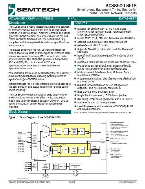
ADVANCED COMMUNICATIONS FINALSynchronous Equipment Timing Source forSONET or SDH Network ElementsDATASHEETThe ACS8509 is a highly integrated, single-chip solution for the Synchronous Equipment Timing Source (SETS) function in a SONET or SDH Network Element. The device generates SONET or SDH Equipment Clocks (SEC) and Frame Synchronization clocks. The ACS8509 is fully compliant with the required international specifications and standards.The device supports Free-run, Locked and Holdovermodes. It also supports all three types of reference clock source: recovered line clock, PDH network, and node synchronization. The ACS8509 generates independent SEC and BITS/SSU clocks, an 8 kHz Frame Synchronization clock and a 2 kHz Multi-Frame Synchronization clock.Two ACS8509 devices can be used together in a Master/ Slave configuration mode allowing system protection against a single ACS8509 failure.A microprocessor port is incorporated, providing access to the configuration and status registers for device setup and monitoring.The ACS8509 includes a choice of edge alignment for 8kHz input, as well as a low jitter n x E1/DS1 output mode. The User can choose between OCXO or TCXO to define the Stratum and/or Holdover performance required.Suitable for Stratum 3E*, 3, 4E, 4 and SONET Minimum Clock (SMC) or SONET/SDH Equipment Clock (SEC) applicationsMeets AT&T, ITU-T, ETSI and Telcordia specifications Accepts four individual input reference clocks Generates six output clocksSupports Free-run, Locked and Holdover modes of operationRobust input clock source quality monitoring on all inputsAutomatic “hit-less” source switchover on loss of input Phase build-out for output clock phase continuity during input switchover and mode transitions Microprocessor interface - Intel, Motorola, Serial, Multiplexed, EPROMProgrammable wander and jitter tracking attenuation 0.1 Hz to 20 HzSupport for Master/Slave device configuration alignment and hot/standby redundancy IEEE 1149.1 JTAG Boundary ScanSingle +3.3 V operation, +5 V I/O compatibleOperating temperature (ambient) -40°C to +85°C Available in 100 pin LQFP package.Lead (Pb)-free version available (ACS8509T), RoHS and WEEE compliant.Note...* Meets holdover requirements, lowest bandwidth 0.1Hz.Block DiagramDescriptionFeaturesADVANCED COMMUNICATIONS FINAL DATASHEET Table of ContentsSection Page Description (1)Block Diagram (1)Features (1)Table of Contents (2)Pin Diagram (4)Pin Description (5)Functional Description (8)Local Oscillator Clock (8)Crystal Frequency Calibration (8)Input Interfaces (9)Over-Voltage Protection (9)Input Reference Clock Ports (9)DivN Examples (10)Input Wander and Jitter Tolerance (10)Frame Sync and Multi-Frame Sync Clocks (Part of T OUT0) (12)Output Clock Ports (12)Low-speed Output Clock (T OUT4) (12)High-speed Output Clock (Part of T OUT0) (12)Low Jitter Multiple E1/DS1 Outputs (13)Output Wander and Jitter (13)Phase Variation (14)Phase Build-Out (17)Microprocessor Interface (17)Motorola Mode (17)Intel Mode (17)Multiplexed Mode (17)Serial Mode (17)EPROM Mode (17)Register Set (18)Configuration Registers (18)Status Registers (18)Register Access (18)Interrupt Enable and Clear (18)Register Map (18)Register Map Description (23)Selection of Input Reference Clock Source (36)Forced Control Selection (36)Automatic Control Selection (36)Ultra Fast Switching (37)Clock Quality Monitoring (37)Activity Monitoring (38)Frequency Monitoring (39)Modes of Operation (39)Free-run mode (39)Pre-Locked mode (39)Locked mode (39)Lost_Phase mode (40)Holdover mode (40)Pre-Locked(2) mode (41)Section Page Protection Facility (41)Alignment of Priority Tables in Master and Slave ACS8509 (42)Alignment of the Selection of Reference Sources for T OUT4 Generation in the Master and Slave ACS8509 (42)Alignment of the Phases of the 8 kHz and 2 kHz Clocks in both Master and Slave ACS8509 (42)JTAG (43)PORB (43)Electrical Specification (45)Operating Conditions (45)DC Characteristics (45)Notes for Tables 24 to 30 (51)Input/Output Timing (52)Motorola Mode (53)Intel Mode (55)Multiplexed Mode (57)Serial Mode (59)EPROM Mode (61)Package Information (62)Thermal Conditions (63)Application Information (64)References (65)Abbreviations (65)Trademark Acknowledgements (66)Revision Status/History (67)Ordering Information (68)Disclaimers (68)Contacts (68)Pin DiagramFigure 2ACS8509 Pin Diagram Synchronous Equipment Timing Source for SONET or SDH Network ElementsNote...I = Input, O = Output, P = Power, TTL U = TTL input with pull-up resistor, TTL D = TTL input with pull-down resistor.Pin DescriptionTable 1Power PinsPin Number SymbolI/O Type Description12, 13, 16VD+P -Supply Voltage: Digital supply to gates in analog section, +3.3 Volts ±10%.33, 39VDD_DIFF P -Supply Voltage: Digital supply for differential ports, +3.3 Volts ±10%.44VDD5P-Digital Supply for +5 Volts Tolerance to Input Pins. Connect to +5Volts (±10%) for clamping to +5 Volts. Connect to VDD for clamping to +3.3 Volts. Leave floating for no clamping, input pins tolerant up to +5.5Volts.50, 61, 85, 86 91VDD P -Supply Voltage: Digital supply to logic, +3.3 Volts ±10%.6VA1+P -Supply Voltage: Analog supply to clock multiplying PLL, +3.3 Volts ±10%.19VA2+P -Supply Voltage: Analog supply to output PLLs, +3.3 Volts ±10%.11, 14, 15, 24, 25, 29, 49, 62, 84, 87,92DGNDP- Supply Ground: Digital ground for logic32, 38GND_DIFF P -Supply Ground: Digital ground for differential ports.1, 5,20AGNDP-Supply Ground: Analog grounds.Table 2Not Connected or Internally Connected PinsPin Number SymbolI/O Type Description4, 17, 26NCNC -Not connected: Leave to Float 3, 18, 22, 27, 28, 34, 35, 40, 41, 42, 43, 46, 47, 52, 53, 55, 57, 89, 93, 94, 96, 97, 98ICIC-Internally Connected: Leave to Float.Table 3Other PinsPin Number Symbol I/O Type Description2TRSTITTL DJTAG Control Reset Input: TRST = 1 to enable JTAG Boundary Scan mode. TRST = 0 for Boundary Scan stand-by mode, still allowing correct device operation. If not used connect to GND or leave floating.7TMS ITTL UJTAG Test Mode Select: Boundary Scan enable. Sampled on rising edge of TCK. If not used connect to VDD or leave floating.8INTREQ O TTL/CMOS Interrupt Request: Active High software Interrupt output.9TCK I TTL D JTAG Clock: Boundary Scan clock input. If not used connect to GND or leavefloating. This pin may require a capacitor placed between the pin and thenearest GND, to reduce noise pickup. A value of 10 pF should be adequate,but the value is dependent on PCB layout.10REFCLK I TTL Reference Clock: 12.800 MHz (refer to “Local Oscillator Clock” on page8). 21TDO O TTL/CMOS JTAG Output: Serial test data output. Updated on falling edge of TCK. If notused leave floating.23TDI I TTL U JTAG Input: Serial test data Input. Sampled on rising edge of TCK. If notused connect to VDD or leave floating.30FrSync O TTL/CMOS Output Reference: 8 kHz Frame Sync output (square wave).31MFrSync O TTL/CMOS Output Reference: 2 kHz Multi-Frame Sync output (square wave).36, 37O1POS, O1NEG O PECL/LVDS Output Reference O1: Programmable, default 19.44 MHz. Also 51.84 MHz,77.76 MHz, 155.52 MHz. MHz, default type PECL.45SYNC2K I TTL D Synchronize 2 kHz: Connect to 2 kHz Multi-Frame Sync output of partnerACS8509 in redundancy system.48SEC1I TTL D Input Reference SEC1: Programmable, default 19.44 MHz(Default Priority 7).51SEC2I TTL D Input Reference SEC2 : Programmable, default 19.44 MHz(Default Priority 8).54SEC3I TTL D Input Reference SEC3: Programmable, default (Master mode)1.544/2.048 MHz, default (Slave mode) 6.48 MHz.(Default Priority 11).56SEC4I TTL D Input Reference SEC4 (Priority 13): Programmable, default1.544/2.048MHz (Default Priority 13).58 - 60UPSEL(2:0)I TTL D Microprocessor Select: Configures the interface for a particularmicroprocessor type at reset.63 - 69A(6:0)I TTL D Microprocessor Interface Address: Address bus for the microprocessorinterface registers. A(0) is SDI in Serial mode - output in EPROM mode only. 70CSB I TTL U Chip Select (Active Low): This pin is asserted Low by the microprocessor toenable the microprocessor interface - output in EPROM mode only.71WRB I TTL U Write (Active Low): This pin is asserted Low by the microprocessor toinitiate a write cycle. In Motorola mode, WRB = 1 for Read.72RDB I TTL U Read (Active Low): This pin is asserted Low by the microprocessor toinitiate a read cycle.73ALE I TTL D Address Latch Enable: This pin becomes the address latch enable from themicroprocessor. When this pin transitions from High to Low, the addressbus inputs are latched into the internal registers. ALE = SCLK in Serialmode.74PORB I TTL U Power-On Reset: Master reset. If PORB is forced Low, all internal states arereset back to default values.Pin Number Symbol I/O Type DescriptionPin Number Symbol I/O Type Description75RDY O TTL/CMOS Ready/Data Acknowledge: This pin is asserted High to indicate the devicehas completed a read or write operation.76 - 83AD(7:0)IO TTL D Address/Data: Multiplexed data/address bus depending on themicroprocessor mode selection. AD(0) is SDO in Serial mode.88O2O TTL/CMOS Output Reference 2: Default 6.48 MHz. Also Dig1 (1.544 MHz/2.048 MHzand 2, 4, 8 x), 19.44 MHz, 25.92 MHz90O3O TTL/CMOS Output Reference 3: 19.44 MHz - fixed.95O4O TTL/CMOS Output Reference 4: 1.544/2.048 MHz, (T4 BITS).99MSTSLVB I TTL U Master/Slave Select: Sets the initial power-up state (or state after a PORB)of the Master/Slave selection register, Reg.34, Bit 1. The register statecan be changed after power up by software.100SONSDHB I TTL D SONET or SDH Frequency Select: Sets the initial power-up state (or stateafter a PORB) of the SONET/SDH frequency selection registers, Reg.34, Bit2 and Reg.38, Bit 5 and Bit 6. When set Low, SDH rates are selected(2.048 MHz etc.) and when set High, SONET rates are selected (1.544 MHzetc.) The register states can be changed after power-up by software.The ACS8509 is a highly integrated, single-chip solution for the SETS function in a SONET/SDH Network Element, for the generation of SEC and frame synchronization pulses.In Free-run mode, the ACS8509 generates a stable, low noise clock signal from an internal oscillator.In Locked mode, the ACS8509 selects the most appropriate input reference source and generates a stable, low-noise clock signal locked to the selected reference.In Holdover mode, the ACS8509 generates a stable, low-noise clock signal from the internal oscillator, adjusted to match the last known good frequency of the last selected reference source.In all modes, the frequency accuracy, jitter and drift performance of the clock meet the requirements of ITU G.812[10], G.813[11], G.823[13], and Telcordia GR-1244-CORE[19].The ACS8509 supports all three types of reference clock source: recovered line clock (T IN1), PDH network synchronization timing (T IN2) and node synchronization (T IN3). The ACS8509 generates independent T OUT0 and T OUT4 clocks, an 8 kHz Frame Synchronization clock and a 2 kHz Multi-Frame Synchronization clock.The ACS8509 has a high tolerance to input jitter and wander. The jitter/wander transfer is programmable (0.1 Hz up to 20 Hz cut-off points).The ACS8509 supports protection. Two ACS8509 devices can be configured to provide protection against a single ACS8509 failure.The protection maintains alignment of the two ACS8509 devices (Master and Slave) and ensures that bothACS8509 devices maintain the same priority table, choose the same reference input and generate the T OUT0 clock, the 8 kHz Frame Synchronization clock and the 2 kHz Multi-Frame Synchronization clock with the same phase.The ACS8509 includes a microprocessor port, providing access to the configuration and status registers for device setup and monitoring.Local Oscillator ClockThe Master system clock on the ACS8509 should be provided by an external clock oscillator of frequency 12.80 MHz. The clock specification is important for meeting the ITU/ETSI and Telcordia performance requirements for Holdover mode. ITU and ETSI specifications permit a combined drift characteristic, at constant temperature, of all non-temperature related parameters, of up to 10 ppb per day. The same specifications allow a drift of 1 ppm over a temperature range of 0 to +70°C.Telcordia specifications are somewhat tighter, requiring a non-temperature-related drift of less than 40 ppb per day and a drift of 280 ppb over the temperature range 0 to +50°C.Please contact Semtech for information on crystal oscillator suppliers.Crystal Frequency CalibrationThe absolute crystal frequency accuracy is less important than the stability since any frequency offset can be compensated by adjustment of register values in the IC. This allows for calibration and compensation of any crystal frequency variation away from its nominal value. ±50 ppm adjustment would be sufficient to cope with most crystals, in fact the range is an order of magnitude larger due to the use of two 8-bit register locations. The setting of the conf_nominal_frequency register allows for this adjustment. An increase in the register value increases the output frequencies by 0.02 ppm for each LSB step. The default value (in decimal) is 39321.Functional DescriptionTable 4ITU and ETSI SpecificationParameter ValueTolerance±4.6 ppm over 20 year lifetimeDrift (Frequency Drift over supply voltage range of +2.7 V to +3.3 V)±0.05 ppm/15 seconds @ constant temp.±0.01 ppm/day @ constant temp.±1 ppm over temp. range 0 to +70°CTable 5Telcordia GR-1244 CORE Specification Parameter Value Tolerance±4.6 ppm over 20 year lifetimeDrift (Frequency Drift over supply voltage range of +2.7 V to +3.3 V)±0.05 ppm/15 seconds @ constant temp.±0.04 ppm/15 seconds @ constant temp.±0.28 ppm/over temp. range 0 to +50°CThe minimum being 0 and the maximum 65535, gives a -700ppm to +500 ppm adjustment range of the output frequencies.For example, if the crystal was oscillating at 12.8 MHz +5ppm, then the calibration value in the register to give a -5 ppm adjustment in output frequencies to compensate for the crystal inaccuracy, would be: 39321 - (5 / 0.02) = 39071 (decimal)Input InterfacesThe ACS8509 supports up to four input reference clock sources from input types T IN1, T IN2 and T IN3 using TTL/ CMOS I/O technologies. These interface technologies support +3.3V and +5 V operation.Over-Voltage ProtectionThe ACS8509 may require Over-Voltage Protection on input reference clock ports according to ITU Recommendation K.41. Semtech protection devices are recommended for this purpose (see separate Semtech data book).Input Reference Clock PortsTable6 gives details of the input reference ports, showing the input technologies and the range of frequencies supported on each port; the default spot frequencies and default priorities assigned to each port on power-up or by reset are also shown. Note that SDH and SONET networks use different default frequencies; the network type is pin-selectable using the SONSDHB pin). Specific frequencies and priorities are set by configuration.Although each input port is shown as belonging to one of the types, T IN1, T IN2 or T IN3, they are fully interchangeable as long as the selected speed is within the maximum operating speed of the input port technology.SDH and SONET networks use different default frequencies; the network type is selectable using the config_mode register 34 Hex, bit 2.For SONET, config_mode register 34 Hex, bit 2 = 1, for SDH config_mode register 34 Hex, bit 2 = 0. On power-up or by reset, the default will be set by the state of the SONSDHB pin (pin 100). Specific frequencies and priorities are set by configuration.TTL ports (compatible also with CMOS signals) support clock speeds up to 100 MHz, with the highest spot frequency being 77.76 MHz. The actual spot frequencies supported are:• 2 kHz,• 4 kHz,• 8 kHz (and N x 8 kHz),• 1.544 MHz (SONET)/2.048 MHz (SDH),• 6.48 MHz,• 19.44 MHz,• 25.92 MHz,• 38.88 MHz,• 51.84 MHz,• 77.76 MHz.The frequency selection is programmed via thecnfg_ref_source_frequency register. The internal DPLL will normally lock to the selected input at the frequency of the input, e.g. 19.44MHz will lock the DPLL phase comparisons at 19.44 MHz. It is, however, possible to utilize an internal pre-divider to the DPLL to divide the input frequency before it is used for phase comparisons in the DPLL. This pre-divider can be used in one of 2 ways: 1.Any of the supported spot frequencies can be dividedto 8 kHz by setting the lock8K bit (bit 6) in theappropriate cnfg_ref_source_frequency registerlocation. For good jitter tolerance for all frequencies and for operation at 19.44 MHz and above, uselock8K. It is possible to choose which edge of the8kHz input to lock to, by setting the appropriate bit of the cnfg_control1 register.2.Any multiple of 8 kHz between 1544 kHz to 100 MHzcan be supported by using the DivN feature (bit 7 of the cnfg_ref_source_frequency register). Anyreference input can be set to use DivN independently of the frequencies and configurations of the otherinputs.Any reference input with the DivN bit set in thecnfg_ref_source_frequency register will employ the internal pre-divider prior to the DPLL locking.The cnfg_freq_divn register contains the divider ratio N where the reference input will get divided by (N+1) where 0<N<214-1. The cnfg_ref_source_frequency register must be set to the closest supported spot frequency to the input frequency, but must be lower than the input frequency. When using the DivN feature the post-dividerNotes: (i)TTL ports (compatible also with CMOS signals) support clock speeds up to 100 MHz, with the highest spot frequency being77.76MHz. The actual spot frequencies are: 2 kHz, 4 kHz, 8 kHz (and N x 8 kHz), 1.544 MHz (SONET)/2.048 MHz (SDH), 6.48 MHz,19.44 MHz, 25.92 MHz, 38.88 MHz, 51.84 MHz, 77.76 MHz. SONET or SDH is selected using the SONSDHB pin. When theSONSDHB pin is High SONET is selected, when the SONSDHB pin is Low SDH is selected.(ii)Input port SEC4 is set at 12 on the Master SETS IC and 1 on the Slave SETS IC, as default on power up (or PORB). The default setup of Master or Slave SEC4 priority is determined by the MSTSLVB pin.frequency must be 8 kHz, which is indicated by setting the lock8k bit high (bit 6 in cnfg_ref_source_frequency register). Any input set to DivN must have the frequency monitors disabled (If the frequency monitors are disabled, they are disabled for all inputs regardless of the input configurations, in this case only activity monitoring will take place). Whilst any number of inputs can be set to use the DivN feature, only one N can be programmed, hence all inputs using the DivN feature must require the same division to get to 8 kHz.DivN ExamplesTo lock to 2.000 MHz:1.The cnfg_ref_source_frequency register is set to11XX0001 (binary) to set the DivN, lock8k bits, and the frequency to E1/DS1. (XX = “leaky bucket” ID for this input).2.The cnfg_mode register (34Hex) bit 2 needs to be setto 1 to select SONET frequencies (DS1).3.The frequency monitors are disabled in cnfg_monitorsregister (48Hex) by writing 00 to bits 0 and 1.4.The DivN register is set to F9 Hex (249 decimal).To lock to 10.000 MHz:1.The cnfg_ref_source_frequency register is set to11XX0010 (binary) to set the DivN, lock8k bits, and the frequency to 6.48 MHz. (XX = “leaky bucket” ID for this input).2.The frequency monitors are disabled in cnfg_monitorsregister (48Hex) by writing 00 to bits 0 and 1.3.The DivN register is set to 4E1 Hex (1249 decimal).Input Wander and Jitter ToleranceThe ACS8509 is compliant to the requirements of all relevant standards, principally ITU Recommendation G.825[15], ANSI T1.101-1999[1] and ETSI ETS 300 462-5 (1996)[4].All reference clock inputs have a tight frequency tolerance but a generous jitter tolerance. Pullin, hold-in and pull-out ranges are specified for each input port in Table7. Minimum jitter tolerance masks are specified in Figures 3 and 4, and Tables 8 and 9, respectively. The ACS8509 will tolerate wander and jitter components greater than those shown in Figure3 and Figure4, up to a limit determined by a combination of the apparent long-term frequency offset caused by wander and the eye-closure caused by jitter (the input source will be rejected if the offset pushesTable 6Input Reference Source Selection and Priority TablePort Number ChannelNumber (Bin)Port Type Input PortTechnologyFrequencies Supported DefaultPrioritySEC10111T IN1TTL/CMOS Up to 100 MHz (see Note (i))Default (SONET): 19.44 MHzDefault (SDH): 19.44 MHz8SEC21000T IN1TTL/CMOS Up to 100 MHz (see Note (i))Default (SONET): 19.44 MHzDefault (SDH): 19.44 MHz9SEC31011T IN2TTL/CMOS Up to 100 MHz (see Note (i))Default (Master) (SONET): 1.544 MHzDefault (Master) (SDH): 2.048 MHzDefault (Slave) 6.48 MHz 12/1 (Note (ii))SEC41101T IN2TTL/CMOS Up to 100 MHz (see Note (i))Default (SONET): 1.544 MHzDefault (SDH): 2.048 MHz14the frequency outside the hold-in range for long enough to be detected, whilst the signal will also be rejected if the eye closes sufficiently to affect the signal purity). The “8klock” mode should be engaged for high jitter tolerance according to these masks. All reference clock ports are monitored for quality, including frequency offset and general activity. Single short-term interruptions in selected reference clocks may not causerearrangements, whilst longer interruptions, or multiple, short-term interruptions, will cause rearrangements, as will frequency offsets which are sufficiently large orsufficiently long to cause loss-of-lock in the phase-locked loop. The failed reference source will be removed from the priority table and declared as unserviceable, until its perceived quality has been restored to an acceptable level.The registers sts_curr_inc_offset (address 0C, 0D, 07) report the frequency of the DPLL with respect to the external TCXO frequency. This is a 19-bit signed number with one LSB representing 0.0003 ppm (range of ±80ppm). Reading this regularly can show how the currently locked source is varying in value e.g. due to wander on its input.The ACS8509 performs automatic frequency monitoring with an acceptable input frequency offset range of ±16.6ppm. The ACS8509 DPLL has a programmablefrequency limit of ±80 ppm. If the range is programmed to be > 16.6 ppm, the frequency monitors should be disabled so the input reference source is not automatically rejected as out of frequency range.Notes: (i)The frequency acceptance and generation range will be ±4.6 ppm around the required frequency when the external crystalfrequency accuracy is within a tolerance of ±4.6 ppm.(ii)The fundamental acceptance range and generation range is ± 9.2 ppm with an exact external crystal frequency of 12.8 MHz. This isthe default DPLL range, the range is also programmable from 0 to 80 ppm in 0.08 ppm steps.Table 7Input Reference Source Jitter ToleranceJitter Tolerance Frequency Monitor Acceptance RangeFrequency AcceptanceRange (Pull-in)Frequency AcceptanceRange (Hold-in)Frequency Acceptance Range (Pull-out)G.703±16.6 ppm ±4.6 ppm (see Note (i))±4.6 ppm (see Note (i))±4.6 ppm (see Note (i))G.783G.823±9.2 ppm (see Note (ii))±9.2 ppm (see Note (ii))±9.2 ppm (see Note (ii))GR-1244-COREFigure 3Minimum Input Jitter Tolerance (OC-3/STM-1)Frame Sync and Multi-Frame Sync Clocks (Part of T OUT0)Frame Sync (8 kHz) and Multi-Frame Sync (2 kHz) clocks are provided on outputs “FrSync” and “MFrSync”. The FrSync and MFrSync clocks have a 50:50 mark space ratio. These are driven from the T OUT0 clock. They are synchronized with their counterparts in a secondACS8509 device (if used), using the technique described later.Output Clock PortsThe device supports a set of main output clocks, T OUT0 and T OUT4, and a pair of secondary output clocks, “Frame Sync” and “Multi-Frame Sync”. The two main output clocks, T OUT0 and T OUT4, are independent of each other and are individually selectable. The two secondary output clocks, Frame Sync and Multi-Frame Sync, are derived from T OUT0. The frequencies of the output clocks are selectable from a range of pre-defined spot frequencies and a variety of output technologies are supported, as defined in Table10.Low-speed Output Clock (T OUT4)The T OUT4 clock is supplied on output port O4. This port will provide a TTL/CMOS signal at either 1.544 MHz or 2.048 MHz, depending on the setting of the SONSDHB pin.High-speed Output Clock (Part of T OUT0)The T OUT0 port has multiple outputs. Output O1 is differential and can support clocks up to 155.52 MHz. Output O2 is a TTL/CMOS output with a choice of 11 different frequencies up to 51.84 MHz. Output O3 is a TTL/CMOS output with fixed frequency of 19.44 MHz. Each output is individually configured to operate at the frequencies shown in Table10 (configuration must be consistent between ACS8509 devices for protection-switching to be effective - output clocks will be phase-aligned between devices). Using thecnfg_differential_outputs register, output O1 can be made to be LVDS or PECL compatible.Low Jitter Multiple E1/DS1 OutputsThis feature is activated using the cnfg_control1 register. This sends a frequency of twice the Dig2 rate (see reg addr 39h, bits 7:6) to the APLL instead of the normal 77.76MHz. For this feature to be used, the Dig2 rate must only be set to 12352kHz/16384kHz using the cnfg_T0_output_frequencies register. The normal OC-3 rate outputs are then replaced with E1/DS1 multiple rates. The E1(SONET)/DS1(SDH) selection is made in the same way as for Dig2 using the cnfg_T0_output_enable register.Table11 shows the relationship between primary output frequencies and the corresponding output in E1/DS1 mode, and from which output they are available. Output Wander and JitterWander and jitter present on the output clocks are dependent on:1.The magnitude of wander and jitter on the selectedinput reference clock (in Locked mode).2.The internal wander and jitter transfer characteristic(in Locked mode).3.The jitter on the local oscillator clock.4.The wander on the local oscillator clock (in Holdovermode).Wander and jitter are treated in different ways to reflect their differing impacts on network design. Jitter is always strongly attenuated, whilst wander attenuation can be varied to suit the application and operating state. Wander and jitter attenuation is performed using a digital phase locked loop (DPLL) with a programmable bandwidth. This gives a transfer characteristic of a low pass filter, with a programmable pole. It is sometimes necessary to change the filter dynamics to suit particular circumstances - one example being when locking to a new source, the filter can be opened up to reduce locking time and can then be gradually tightened again to remove wander. Since wander represents a relatively long-term deviation from the nominal operating frequency, it affects the rate of supply of data to the network element. Strong wander attenuation limits the rate of consumption of data to within a smaller range, so a larger buffer store is required to prevent data loss. But, since any buffer store potentially。
ZXCT1010_电流监控芯片

1ISSUE 10 - JULY 2007S E M I C O N D U C T O R SZXCT1010DESCRIPTIONThe ZXCT1010is a high side current sense ing this device eliminates the need to disrupt the ground plane when sensing a load current.It is an enhanced version of the ZXCT1009offering reduced typical output offset and improved accuracy at low sense voltage.The wide input voltage range of 20V down to as low as 2.5V make it suitable for a range of applications.A minimum operating current of just 4µA,combined with its SOT23-5package make suitable for portable battery equipment.FEATURES •Low cost, accurate high-side current sensing •Output voltage scaling •Up to 2.5V sense voltage • 2.5V – 20V supply range •300nA typical offset current • 3.5µA quiescent current •1% typical accuracy •SOT23 -5 packageAPPLICATIONS •Battery chargers •Smart battery packs •DC motor control •Over current monitor •Power management•Programmable current sourceENHANCED HIGH-SIDE CURRENT MONITORAPPLICATION CIRCUITDEVICE REEL SIZE TAPE WIDTH QUANTITY PERREEL ZXCT1010E5TA7”8mm3,000 unitsPARTMARK 101PACKAGESOT23-5ORDERING INFORMATIONZXCT1010ABSOLUTE MAXIMUM RATINGSVoltage on any pin-0.6V to 20V (relative to GND)Continuous output current, I OUT,25mAContinuous sense voltage, V SENSE2,-0.5V to +5VOperating temperature, T A,-40 to 85°CStorage temperature-55 to 150°CPackage power dissipation(T A= 25°C)SOT23-5300mWOperation above the absolute maximum rating may cause device failure.Operation at the absolute maximum ratings, for extended periods, may reduce device reliability. ELECTRICAL CHARACTERISTICSTest Conditions T A= 25°C, V in= 5V, R out= 100Ω.SYMBOL PARAMETER CONDITIONS LIMITS UNITMin Typ Max V in V CC Range 2.520VI out1Output current V sense=0VV sense=10mVV sense=100mVV sense=200mVV sense=1V 0850.9751.959.70.31001.002.0010.0101151.0252.0510.3µAµAmAmAmAI q Ground pincurrentV sense=0V 3.58µA V sense2Sense Voltage02500mV I sense-V sense-input current100nA Acc Accuracy R sense=0.1ΩV sense=200mV-2.5 2.5% Gm Transconductance,I out/V sense10000µA/VBW Bandwidth V SENSE(DC)=10mV,Pin=-40dBm‡V SENSE(DC)=100mV,Pin=-20dBm‡3002kHzMHz1Includes input offset voltage contribution2VSENSE is defined as the differential voltage between V SENSE+and V SENSE-.V SENSE= V SENSE+- V SENSE-= V IN- V LOAD= I LOAD x R SENSE3-20dBm=63mVp-p into 50ΩISSUE 10 - JULY 2007S E M I C O N D U C T O R SZXCT1010TYPICAL CHARACTERISTICSISSUE 10 - JULY 20073S E M I C O N D U C T O R SZXCT1010PIN DESCRIPTIONPin Name Pin FunctionV sense+Supply voltageV sense-Connection to load/batteryI out Output current,proportional to V in-V loadGND GroundCONNECTION DIAGRAMSCHEMATIC DIAGRAMISSUE 10 - JULY 20074S E M I C O N D U C T O R SISSUE 10 - JULY 2007S E M I C O N D U C T O R SZXCT10105The following lines describe how to scale a load current to an output voltage.V sense = V in -V load V out = 0.01 x V sense x R out 1E.g.A 1A current is to be represented by a 100mV output voltage:1)Choose the value of R sense to give 50mV >V sense >500mV at full load.For example V sense =100mV at 1.0A.R sense =0.1/1.0=> 0.1 ohms.2)Choose R out to give V out =100mV,when V sense =100mV.Rearranging 1for R out gives:R out =V out /(V sense x 0.01)R out =0.1/(0.1x 0.01)=100ΩTYPICAL CIRCUIT APPLICATIONPOWER DISSIPATIONThe maximum allowable power dissipation of the device for normal operation (Pmax),is a function of the package junction to ambient thermal resistance (θja),maximum junction temperature (Tjmax),and ambient temperature (Tamb),according to the expression:P max = (Tj max – T amb ) /θjaThe device power dissipation,P D is given by the expression:P D =I out .(V in -V out ) WattsWhere R load represents any load including DC motors,a charging battery or further circuitry that requires monitoring,R sense can be selected on specific requirements of accuracy, size and power rating.APPLICATIONS INFORMATIONISSUE 10 - JULY 2007S E M I C O N D U C T O R SZXCT10106Li-Ion Charger CircuitThe above figure shows the ZXCT1010supporting the Benchmarq bq2954Charge Management IC.Most of the support components for the bq2954are omitted for clarity.This design also uses the Zetex FZT789A high current Super-PNP as the switching transistor in the DC-DC step down converter and the FMMT451as the drive NPN for the FZT789A.The circuit can be configured to charge up to four Li-Ion cells at a charge current of 1.25A.Charge can be terminated on maximum voltage,selectable minimum current,or maximum time out.Switching frequency of the PWM loop is approximately 120kHz.APPLICATIONS INFORMATION (Continued)Bi-Directional Current SensingThe ZXCT1010can be used to measure current bi-directionally,if two devices are connected as shown below.If the voltage V1is positive with respect to the voltage V2the lower device will be active,delivering a proportional output current to Rout.Due to the polarity of the voltage across Rsense,the upper device will be inactive and will not contribute to the current delivered to Rout.When V2is morepositive than V1,current will be flowing in the opposite direction,causing the upper device to be active instead.Non-linearity will be apparent at small values of Vsense due to offset current contribution.Devices can use separate output resistors if the current direction is to be monitored independently.Bi-directional Transfer Function-400-200020040012345O u t p u t C u r r e n t (m A )Sense Voltage (mV)Output Current v Sense VoltageISSUE 10 - JULY 2007S E M I C O N D U C T O R SZXCT10107PCB trace shunt resistor for low cost solutionThe figure below shows output characteristics of the device when using a PCB resistive trace for a low cost solution in replacement for a conventional shunt resistor.The graph shows the linear rise in voltage across the resistor due to the PTC of the material and demonstrates how this rise in resistance value over temperature compensates for the NTC of the device.The figure opposite shows a PCB layout suggestion.The resistor section is 25mm x 0.25mm giving approximately 150m Ωusing 1oz copper.The data for the normalised graph was obtained using a 1A load current and a 100Ωoutput resistor.An electronic version of the PCB layout is available at/isenseAPPLICATIONS INFORMATION (Continued)Layout shows area of shunt resistor compared to SOT23-5package. Not actual sizeActual SizeZXCT1010DefinitionsProduct changeZetex Semiconductors reserves the right to alter,without notice,specifications,design,price or conditions of supply of any product or service. Customers are solely responsible for obtaining the latest relevant information before placing orders.Applications disclaimerThe circuits in this design/application note are offered as design ideas.It is the responsibility of the user to ensure that the circuit is fit for the user's application and meets with the user's requirements.No representation or warranty is given and no liability whatsoever is assumed by Zetex with respect to the accuracy or use of such information,or infringement of patents or other intellectual property rights arising from such use or otherwise.Zetex does not assume any legal responsibility or will not be held legally liable(whether in contract,tort(including negligence), breach of statutory duty,restriction or otherwise)for any damages,loss of profit,business,contract,opportunity or consequential loss in the useof these circuit applications,under any circumstances.Life supportZetex products are specifically not authorized for use as critical components in life support devices or systems without the express written approval of the Chief Executive Officer of Zetex Semiconductors plc.As used herein:A.Life support devices or systems are devices or systems which:1.are intended to implant into the bodyor2.support or sustain life and whose failure to perform when properly used in accordance with instructionsfor use provided in the labeling can be reasonably expected to result in significant injury to the user.B.A critical component is any component in a life support device or system whose failure to perform can be reasonably expected to cause the failure of the life support device or to affect its safety or effectiveness.ReproductionThe product specifications contained in this publication are issued to provide outline information only which(unless agreed by the company in writing)may not be used,applied or reproduced for any purpose or form part of any order or contract or be regarded as a representation relatingto the products or services concerned.Terms and ConditionsAll products are sold subjects to Zetex'terms and conditions of sale,and this disclaimer(save in the event of a conflict between the two when the terms of the contract shall prevail)according to region,supplied at the time of order acknowledgement.For the latest information on technology,delivery terms and conditions and prices,please contact your nearest Zetex sales office.Quality of productZetex is an ISO9001and TS16949certified semiconductor manufacturer.To ensure quality of service and products we strongly advise the purchase of parts directly from Zetex Semiconductors or one of our regionally authorized distributors.For a complete listing of authorized distributors please visit:/salesnetworkZetex Semiconductors does not warrant or accept any liability whatsoever in respect of any parts purchased through unauthorized sales channels.ESD(Electrostatic discharge)Semiconductor devices are susceptible to damage by ESD.Suitable precautions should be taken when handling and transporting devices.The possible damage to devices depends on the circumstances of the handling and transporting,and the nature of the device.The extent of damage can vary from immediate functional or parametric malfunction to degradation of function or performance in use over time.Devices suspected of being affected should be replaced.Green complianceZetex Semiconductors is committed to environmental excellence in all aspects of its operations which includes meeting or exceeding regulatory requirements with respect to the use of hazardous substances.Numerous successful programs have been implemented to reduce the use of hazardous substances and/or emissions.All Zetex components are compliant with the RoHS directive,and through this it is supporting its customers in their compliance with WEEE andELV directives.Product status key:"Preview"Future device intended for production at some point.Samples may be available"Active"Product status recommended for new designs"Last time buy(LTB)"Device will be discontinued and last time buy period and delivery is in effect"Not recommended for new designs"Device is still in production to support existing designs and production"Obsolete"Production has been discontinuedDatasheet status key:"Draft version"This term denotes a very early datasheet version and contains highly provisionalinformation,which may change in any manner without notice."Provisional version"This term denotes a pre-release datasheet.It provides a clear indication of anticipated performance.However,changes toISSUE 10 - JULY 20078S E M I C O N D U C T O R SZXCT1010S E M I C O N D U C T O R SISSUE 10 - JULY 20079EuropeZetex GmbHKustermann-Park Balanstraße 59D-81541 München GermanyTelefon: (49) 89 45 49 49 0Fax: (49) 89 45 49 49 49europe.sales@AmericasZetex Inc700 Veterans Memorial Hwy Hauppauge, NY 11788USATelephone: (1) 631 360 2222Fax: (1) 631 360 8222usa.sales@Asia PacificZetex (Asia) Ltd3701-04Metroplaza Tower 1Hing Fong Road, Kwai Fong Hong KongTelephone: (852) 26100 611Fax: (852) 24250 494asia.sales@Corporate Headquarters Zetex Semiconductors plc Zetex Technology ParkChadderton, Oldham, OL9 9LL United KingdomTelephone (44) 161 622 4444Fax: (44) 161 622 4446hq@©ZetexSemiconductors plc 2007PAD LAYOUT DETAILSPACKAGE DIMENSIONSControlling dimensions are in millimeters. Approximate conversions are given in inchesPACKAGE DIMENSIONS。
电子元器件ZXCT1050中文资料_数据手册_IC数据表

ZXCT1050Precision wide input range current monitorDescriptionOrdering informationThe ZXCT1050 is a wide input range current monitor, which operates over a range of input voltages from ground up to V CC -2V. As a result the ZXCT1050 can be used on the high or low side of the load.The ZXCT1050 provides variable gain by using two external resistors. The first of which sets the transconductance and the second setting the overall gain.The very low offset voltage enables a typical accuracy of 1% for sense voltages of only 30mV,giving better tolerances for small sense resistors necessary at higher currents.Features•Accurate down to end current sensing •Output voltage scaling x10•0 to V CC -2V sense input range • 2.7 to 20V supply range •50µA quiescent current •SOT23-5 packageApplications•Power supply•DC motor and solenoid control •Battery management •Over current monitor •Power management •Short circuit detectionPin connectionsTypical application circuitOrder code Pack Part mark Reel size(inches)Tape width (mm)Quantity per reel ZXCT1050E5TASOT23-51050783000Absolute maximum ratingsV CC max.20V Voltage on SENSE- and SENSE+-0.6 to V CCVoltage on all other pins -0.6V and V CC +0.6V V SENSE = ‘(V SENSE +) - (V SENSE -)’500mV Operating temperature -40 to 125°C Storage temperature-55 to 150°C Maximum junction temperature 150°CPackage power dissipation300mW * at T A = 25°C (De-rate to zero for T J = 150°C)Operation above the absolute maximum rating may cause device failure. Operation at the absolute maximum ratings, for extended periods, may reduce device reliability.Recommended operating conditionsRecommended resistor gain setting combinationsPin function tableParameterMin.Max.Units V SENSE+Common-mode sense input range 0V CC -2V V CC Supply voltage range2.720V V SENSE Differential sense input voltage range 10300mV V OUTOutput voltage range 0V CC -2V T AAmbient temperature range-40125°CGain R SH R G 107.5k ⍀ 3.75k ⍀207.5k ⍀7.5k ⍀507.5k ⍀18.7k ⍀1007.5k ⍀37.5k ⍀20 3.75k ⍀ 3.75k ⍀50 1.5k ⍀ 3.75k ⍀100750⍀3.75k ⍀PIN Name Description1V CC This is the analog supply and provides power to internal circuitry.2GND Ground pin.3OUT Output pin. A resistor, R GAIN , connected from this pin pin down to ground develops an output voltage.4SENSE+This is the positive input of the current monitor and has an input range from 0V up to V CC – 2V.5SENSE-This is the negative input of the current monitor and has an input range from 0V up to V CC – 2V. The current through this pin varies with differential sense voltage. A resistor, R SHUNT , from this pin to the rail being sensed set the transconductance of the current monitor.Electrical characteristicsTest conditions T A = 25°C, V SENSE+ = 10V, V CC = 12V, V SENSE = 100mV, R SH = 7.5k ⍀, R G = 3.75k ⍀.SymbolParameter Conditions Min.Typ.Max.Units I Q V CC pin current V SENSE = 0V 4570µA V OUTOutput voltageV SENSE = 0V =30mV =100mV =150mV02850.971.4533001.001.50153151.031.55mVmV V V I SENSE+V SENSE+ input current V SENSE = 0V 60150nA I SENSE-V SENSE- input current V SENSE = 0V 15150nA V OUT TC V OUT variation with temperature See note (*)NOTES:(*)Temperature dependent measurements are extracted from characterisation and simulation results.300ppm/°CGain V OUT /V SENSE 10Accuracy Total output error -33%BWBandwidthV SENSE(DC) = 10mV V SENSE(AC) = 10mV PPCL = 5pF , 300kHz VSENSE(DC)= 100mV0.8MHz PSRR Power supply rejection ratio V CC = 2.7V to 20V V SENSE+ = 0.7V 60dB CMRRCommon mode rejection ratioV CC = 20VV SENSE+ = 0 to 18V70dBTypical characteristicsR G = 3.75k⍀, R SH = 7.5k⍀ unless otherwise stated.Typical characteristicsR G = 3.75k⍀, R SH = 7.5k⍀ unless otherwise stated.Typical characteristicsR G = 3.75k⍀, R SH = 7.5k⍀ unless otherwise stated.Applications informationThe ZXCT1050 is a current output version of the ZXCT1051 and as such uses a separate power supply pin. All biasing for the internal amplifiers comes from its separate V CC input and is not ‘line powered’, unlike the ZXCT1021.This means that at very small sense voltages the ZXCT1050 draws very little current (<1A) from the lines being sensed.The separate V CC pin enables the ZXCT1050 to be operated at sense line voltages down to 0V,where the ZXCT1021 would switch off. This feature enables the ZXCT1050 to be used to sense the currents flowing through lines that have been shorted to ground.Basic operationLoad current, I L , from V RAIL is drawn through R SENSE developing a voltage V SENSE across the sense inputs of the ZXCT1050.The internal amplifier forces V SENSE across external resistance R SH (internal on the ZXCT1051)causing a current to flow through transistor Q1 and out of the output pin, OUT. This current is then converted to a voltage by a resistor, R G , between OUT and GND.The overall gain of the ZXCT1050 is determined by the following expression:A ratio of 1:2 between R SH and R G creates the fixed gain of 10 with an output impedance equal to RG (see electrical characteristics for output current-voltage characteristics).The ZXCT1050 has both R G and R SH external. This allows R G and R SH to be varied so that the required gain can be achieved at the required output impedance.For low power applications both R G and R SH can be increased whereas for driving low impedance R G and R SH can be decreased.The maximum recommended value for R G is 40k ⍀ and the maximum recommended value for RSH is 10k ⍀. Large values of R SH start increasing the effective input offset error, while large values of R G can created load errors and reduce bandwidths.The maximum differential input voltage, V SENSE , is 150mV (I L * R SENSE ); however voltages up to 500mV will not damage it. This can be increased further by the inclusion of a resistor, R LIM ,between the SENSE+ pin and the rail being sensed, V RAIL .For best performance R SENSE should be connected as close to the SENSE+ and SENSE- pins thus minimizing any series resistance with R SENSE .GAIN 20R GR SH----------×=Package outline - SOT23-5Note: Controlling dimensions are in millimeters. Approximate dimensions are provided in inchesDIM MillimetersInchesMin.Max.Min.Max.A - 1.00-0.0393A10.010.100.00030.0039A20.840.900.03300.0354b 0.300.450.01180.0177c 0.120.200.00470.0078D 2.90 BSC 0.114 BSCE 2.80 BSC 0.110 BSC E1 1.60 BSC 0.062 BSC e 0.95 BSC 0.0374 BSC e1 1.90 BSC0.0748 BSCL 0.300.500.01180.0196L20.25 BSC 0.010 BSCa°4°12°4°12°DefinitionsProduct changeZetex Semiconductors reserves the right to alter, without notice, specifications, design, price or conditions of supply of any product or service. Customers are solely responsible for obtaining the latest relevant information before placing orders.Applications disclaimerThe circuits in this design/application note are offered as design ideas. It is the responsibility of the user to ensure that the circuit is fit for the user’s application and meets with the user’s requirements. No representation or warranty is given and no liability whatsoever is assumed by Zetex with respect to the accuracy or use of such information, or infringement of patents or other intellectual property rights arising from such use or otherwise. Zetex does not assume any legal responsibility or will not be held legally liable (whether in contract, tort (including negligence), breach of statutory duty, restriction or otherwise) for any damages, loss of profit, business, contract, opportunity or consequential loss in the use of these circuit applications, under any circumstances.Life supportZetex products are specifically not authorized for use as critical components in life support devices or systems without the express written approval of the Chief Executive Officer of Zetex Semiconductors plc. As used herein:A. Life support devices or systems are devices or systems which:1.are intended to implant into the bodyor2.support or sustain life and whose failure to perform when properly used in accordance with instructions for use provided in thelabelling can be reasonably expected to result in significant injury to the user.B. A critical component is any component in a life support device or system whose failure to perform can be reasonably expected tocause the failure of the life support device or to affect its safety or effectiveness.ReproductionThe product specifications contained in this publication are issued to provide outline information only which (unless agreed by the company in writing) may not be used, applied or reproduced for any purpose or form part of any order or contract or be regarded as a representation relating to the products or services concerned.Terms and ConditionsAll products are sold subjects to Zetex’ terms and conditions of sale, and this disclaimer (save in the event of a conflict between the two when the terms of the contract shall prevail) according to region, supplied at the time of order acknowledgement.For the latest information on technology, delivery terms and conditions and prices, please contact your nearest Zetex sales office.Quality of productZetex is an ISO 9001 and TS16949 certified semiconductor manufacturer.To ensure quality of service and products we strongly advise the purchase of parts directly from Zetex Semiconductors or one of our regionally authorized distributors. For a complete listing of authorized distributors please visit: /salesnetworkZetex Semiconductors does not warrant or accept any liability whatsoever in respect of any parts purchased through unauthorized sales channels. ESD(Electrostatic discharge)Semiconductor devices are susceptible to damage by ESD. Suitable precautions should be taken when handling and transporting devices. The possible damage to devices depends on the circumstances of the handling and transporting, and the nature of the device. The extent of damage can vary from immediate functional or parametric malfunction to degradation of function or performance in use over time. Devices suspected of being affected should be replaced.Green complianceZetex Semiconductors is committed to environmental excellence in all aspects of its operations which includes meeting or exceeding regulatory requirements with respect to the use of hazardous substances. Numerous successful programs have been implemented to reduce the use of hazardous substances and/or emissions.All Zetex components are compliant with the RoHS directive, and through this it is supporting its customers in their compliance with WEEE and ELV directives.Product status key:“Preview”Future device intended for production at some point. Samples may be available“Active”Product status recommended for new designs“Last time buy (LTB)”Device will be discontinued and last time buy period and delivery is in effect“Not recommended for new designs”Device is still in production to support existing designs and production“Obsolete”Production has been discontinuedDatasheet status key:“Draft version”This term denotes a very early datasheet version and contains highly provisional information, whichmay change in any manner without notice.“Provisional version”This term denotes a pre-release datasheet. It provides a clear indication of anticipated performance.However, changes to the test conditions and specifications may occur, at any time and without notice.“Issue”This term denotes an issued datasheet containing finalized specifications. However, changes tospecifications may occur, at any time and without notice.。
液晶显示器芯片mp1009资料

MP1009Nu-Pulse TM , Half-Bridge and Push-PullCCFL Inverter ControllerPRELIMINARY SPECIFICATIONS SUBJECT TO CHANGEMPS CONFIDENTIAL AND PROPRIETARY INFORMATION – INTERNAL USE ONLYThe Future of Analog IC TechnologyDESCRIPTIONThe MP1009 is a fixed operating frequencyFEATURES• Drives Two External, Low Cost, N-ChannelMPS CONFIDENTIAL AND PROPRIETARY INFORMATION – INTERNAL USE ONLYORDERING INFORMATIONPart Number*Package Top Marking Free Air Temperature (T A) MP1009ES SOIC16 MP1009ES-20°C to +85°CABSOLUTE MAXIMUM RATINGS Input Voltage VIN.........................................-0.3V to VIN+VCC-0.3V to VIN0.3V to +6.5V0.3V to +6.5V5.8V to +5.8V OV1 and OV2 inputs..................-0.3V to +14.5V= +25°C) (2).......................................................1.56W Junction Temperature. (150)Power Dissipation......................................0.6W Lead Temperature (Solder).. (260)Operating Frequency.............................150kHzC to +150Recommended Operating Conditions Input Voltage VDigital Brightness Voltage VOperating Frequency..............Operating Frequency (Typical)Operating Junct. Temp (TSOIC16 (80)Notes:1) ExceedingThe maximum allowable power dissipation is a function of the maximum junction temperature Tambient thermal resistanceA. The maximum allowable continuous power dissipation at any ambient temperature is calculated by P(MAX)-T A)/dissipation will cause excessive die temperature, and the regulator will go into thermal shutdown. Internal thermal shutdown circuitry protects the device from permanent damage.3) The device is not guaranteed to function outside of itsoperating conditions.4) Measured on JESD51-7, 4-layer PCB.ELECTRICAL CHARACTERISTICSV IN = 17.5V, T A = +25°C, unless otherwise noted.ELECTRICAL CHARACTERISTICS (continued) V = 17.5V, T = +25°C, unless otherwise noted.PIN FUNCTIONSPIN FUNCTIONS (continued)OPERATIONThe MP1009 is a fixed frequency inverter controller for CCFL application, especially optimized for multi-lamp applications. The The maximum frequency under this operation mode is set to be 1.4 times of normal frequency. Fault ProtectionWhen the lamp is open, the voltage feedback on OV1 and OV2 pin is used to regulate the lamp voltage. The voltage feedback on OV1 is higher than 150°C, it shuts down the whole chip. When the temperature is lower than its lower threshold, typically 145°C, the chip is enabled again.APPLICATION INFORMATIONThe typical 4-lamp half bridge application circuit is used as an example to describe the design procedure.Open lamp protection with LI1/LI2 Also, the lamp current feedback signal on LI1/LI2 pin is compared to internal 1.1V reference before the internal resistor divider. In normal operation, the voltage waveform should be sinusoidal waveforms. In open lamp condition, the positive half cycle will be missed as shown in Figure 2, which will trigger the open lamp protection. Pin1 (OV2) & Pin 16 (OV1): Lamp Voltage Regulation and Short Circuit ProtectionOV1 and OV2 are used for lamp voltage feedback and short circuit protection with the unique protection method (patent protected).Short Circuit protection withOV1/OV2The regulated open lamp voltage is proportional to the ratio of C1 to C2 (also, C3 to C4, C5 to C6 and C7 to C8).C1 has to be rated at 3kV and is typically between 5pF to 22pF. The value of C2 is set byMPS CONFIDENTIAL AND PROPRIETARY INFORMATION – INTERNAL USE ONLYcustomer to program the required open lamp voltage. The value of DC bias resistors (R5~R8) is typically 10kΩ.For safety operation, V PP for normal operation For a C12=820nF, then the time out for open lamp is 0.98s. For short circuit:The internal current for short circuit protection is 100uA instead of 1uA for open lamp protection, the off time will be approximately 100 times Figure 5—Burst Mode with DC input voltageat DBRT pin.MPS CONFIDENTIAL AND PROPRIETARY INFORMATION – INTERNAL USE ONLYR10 and C14 can be estimated by the following equations:1R1021.16k Ω-1+21.43k Ω⎛⎞≈⎜⎟Pin 9 (VIN): C15, C18 Input Power RailAn electrolytic capacitor and a ceramic capacitor are recommended between VIN and power ground. The ceramic capacitor C18 should be placed close to the MOSFETs toMPS CONFIDENTIAL AND PROPRIETARY INFORMATION – INTERNAL USE ONLY TYPICAL APPLICATION CIRCUITMPS CONFIDENTIAL AND PROPRIETARY INFORMATION – INTERNAL USE ONLY PACKAGE INFORMATIONSOIC16NOTICE: The information in this document is subject to change without notice. Users should warrant and guarantee that third party Intellectual Property rights are not infringed upon when integrating MPS products into any application. MPS will not assume any legal responsibility for any said applications.。
中国电信移动终端测试规范-CDMA_GSM双模终端分册2009.V1
保密等级:公开发放中国电信正式版目录目录..........................................................................................................................................I 前言.......................................................................................................................................IV 1适用范围..................................................................................................................................1 2参考资料 (1)3 名词和缩略语 (1)3.1 名词....................................................................................................................................1 3.2 缩略语................................................................................................................................1 4 概述 (1)4.1 测试等级 (2)4.2 测试结果判断准则 (2)4.2.1 预期结果的测试结果判断准则 (2)4.2.2 测试用例的测试结果判断准则 (3)4.3 测试编号组成 (3)5 测试环境和素材 (4)5.1测试环境............................................................................................................................4 5.2测试配置参数....................................................................................................................4 5.3测试仪器仪表....................................................................................................................4 5.4 测试素材............................................................................................................................4 6 双模双待终端测试要求. (5)6.1 选网选卡 (5)6.1.1 TC-CDMA/GSM-01001 [必选] 双模双待终端卡槽要求 (5)6.1.2 TC-CDMA/GSM-01002 [必选] 双模双待终端开机选网要求 (5)6.1.3 TC-CDMA/GSM-01003 [必选] 双模双待终端卡网络选择菜单要求 (6)6.1.4 TC-CDMA/GSM-01004 [必选] 双模双待终端待机选网要求 (7)6.2 基本功能 (8)6.2.1 TC-CDMA/GSM-01005 [必选] 双模双待终端紧急呼叫功能要求 (8)6.2.2 TC-CDMA/GSM-01006 [必选] 双模双待终端时钟要求 (9)6.2.3 TC-CDMA/GSM-01007 [必选] 双模双待终端CDMA 模式下+号处理要求 (10)6.2.4 TC-CDMA/GSM-01008 [必选] 双模双待终端GSM 模式下+号处理要求 (11)6.2.5 TC-CDMA/GSM-01009 [必选] 双模双待终端短信存取要求 (11)6.2.6 TC-CDMA/GSM-01010 [必选] 双模双待终端电话本存取要求 (13)6.2.7 TC-CDMA/GSM-01011 [必选] 双模双待终端文件夹存取要求 (14)6.2.8 TC-CDMA/GSM-01012 [必选] 双模双待终端通话记录存取要求 (15)中国电信正式版6.3 与卡交互功能 (16)6.3.1 TC-CDMA/GSM-01013 [必选] 双模双待终端卡应用菜单与命令 (16)6.3.2 TC-CDMA/GSM-01014 [必选] 双模双待终端GSM 模式下OTA 短信要求 (16)6.4 协议与射频 (17)6.4.1 TC-CDMA/GSM-01015 [必选] 双模双待终端CG 双待下发射机互扰要求 (17)6.4.2 TC-CDMA/GSM-01016 [必选] 双模双待终端GSM 侧数据业务 (18)6.5 业务要求 (18)6.5.1 TC-CDMA/GSM-01017 [必选] 双模双待终端CG 双待且双模空闲场景时业务并发 186.5.2 TC-CDMA/GSM-01018 [必选] 双模双待终端CG 双待G 通话场景时业务并发..206.5.3 TC-CDMA/GSM-01019 [必选] 双模双待终端CG 双待C 通话场景时业务并发 (22)6.5.4 TC-CDMA/GSM-01020 [必选] 双模双待终端CG 双待C 数据场景时业务并发 (23)6.5.5 TC-CDMA/GSM-01021 [必选] 双模双待终端GSM 模式USSD 功能要求 (24)6.6 UI 要求 (25)6.6.1 TC-CDMA/GSM-01022 [必选] 双模双待终端模式与网络显示要求 (25)6.6.2 TC-CDMA/GSM-01023 [推荐] 双模双待终端菜单及资源要求 (25)6.7 安全性要求 (26)6.7.1 TC-CDMA/GSM-01024 [必选] 双模双待终端PIN 码处理 (26)7 双模单待终端测试要求 (27)7.1 选网选卡 (27)7.1.1 TC-CDMA/GSM-02001 [必选] 双模单待终端卡槽要求 (27)7.1.2 TC-CDMA/GSM-02002 [必选] 双模单待终端开机选网要求 (28)7.1.3 TC-CDMA/GSM-02003 [必选] 双模单待终端卡网络选择菜单要求 (28)7.1.4 TC-CDMA/GSM-02004 [必选] 双模单待终端搜网不成功网络切换菜单 (29)7.1.5 TC-CDMA/GSM-02005 [必选] 双模单待终端待机选网要求 (29)7.2 基本功能要求 (30)7.2.1 TC-CDMA/GSM-02006 [必选] 双模单待终端紧急呼叫功能要求 (30)7.2.2 TC-CDMA/GSM-02007 [必选] 双模单待终端时钟要求 (31)7.2.3 TC-CDMA/GSM-02008 [必选] 双模单待终端CDMA 模式下+号处理要求 (31)7.2.4 TC-CDMA/GSM-02009 [必选] 双模单待终端GSM 模式下+号处理要求 (32)7.2.5 TC-CDMA/GSM-02010 [必选] 双模单待终端短信存取要求 (32)7.3 与卡交互功能 (33)7.3.1 TC-CDMA/GSM-02011 [必选] 双模单待终端卡应用菜单与命令 (33)7.3.2 TC-CDMA/GSM-02012 [必选] 双模单待终端GSM 模式OTA 短信功能要求 (34)7.4 业务要求 (34)7.4.1 TC-CDMA/GSM-02013 [必选] 双模单待终端GSM 模式USSD 功能要求 (34)7.4.2 TC-CDMA/GSM-02014 [必选] 双模单待终端GSM 侧数据业务 (34)7.5 UI 要求 (35)7.5.1 TC-CDMA/GSM-02015 [必选] 双模单待终端模式与网络显示要求 (35)7.5.2 TC-CDMA/GSM-07016 [推荐] 双模单待终端菜单及资源要求...............................36 8详细更新历史 (36)中国电信正式版图目录图 5-1:测试环境 (4)表目录表4-1:要求等级...........................................................................................................................2 表4-2:用例的测试结果判断准则...............................................................................................3 表5-1:测试仪器仪表...................................................................................................................4 表5-2:测试素材 (4)中国电信正式版前 言本规范是中国电信移动终端测试规范体系的系列规范之一,该系列规范主要包括但不限于以下分册:(1) 中国电信移动终端测试规范-基本技术要求分册(2) 中国电信移动终端测试规范-SMS 分册(3) 中国电信移动终端测试规范-MMS 分册(4) 中国电信移动终端测试规范-Java 分册(5) 中国电信移动终端测试规范-BREW 分册(6) 中国电信移动终端测试规范-流媒体分册(7) 中国电信移动终端测试规范-全功能浏览器分册 (8) 中国电信移动终端测试规范-浏览器分册(9) 中国电信移动终端测试规范-LBS 分册(10) 中国电信移动终端测试规范-PIM 分册(11) 中国电信移动终端测试规范-CDMA/GSM 双模终端分册(12) 中国电信移动终端测试规范-DM 分册 (13) 中国电信移动终端测试规范-DRM 分册(14) 中国电信移动终端测试规范-Email 分册(15) 中国电信移动终端测试规范-条码分册 (16) 中国电信移动终端测试规范-1xEVDO 混合操作要求分册(17) 中国电信移动终端测试规范-Rev.0现网测试要求分册 (18) 中国电信移动终端测试规范-Rev.A 现网测试要求分册(19) 中国电信移动终端测试规范-Rev.A 数据终端测试要求分册(20) 中国电信移动终端测试规范-最低射频性能要求分册(21) 中国电信移动终端测试规范-最低数据性能要求分册(22) 中国电信移动终端测试规范-最低协议一致性要求分册(23) 中国电信移动终端测试规范-UI 分册本规范是中国电信终端测评体系CDMA 终端测试系列的组成部分之一,描述了CDMA/GSM 双模终端基本要求的测试环境、测试素材、测试用例和测试结果判定准则。
中国电信集团公司C网网络优化培训材料

中国电信集团公司C网网络优化培训材料中博信息技术研究院2020年5月修订记录前言为了配合中国电信网优中心开展的网优人员认证工作,特编订本教材,由于编者学识有限,偏颇和不当之处在所难免,敬请各位网优人员不吝赐教,为修订工作提供宝贵意见。
目录第1章基站系统主设备——中兴篇 (8)1.1 中兴基站ZXSDR BS8800 (8)1.1.1 BS8800在网络中的位置 (8)1.1.2 BS8800系统组成 (8)1.1.3 BS8800硬件结构 (9)1.1.4 BS8800工作原理 (13)1.1.5 BS8800要紧技术指标 (14)1.2 中兴基站ZXC10 CBTS I2 (14)1.2.1 CBTS I2在网络中的位置 (14)1.2.2 CBTS I2系统组成 (15)1.2.3 CBTS I2硬件结构 (16)1.2.4 CBTS I2工作原理 (20)1.2.5 CBTS I2要紧技术指标 (22)1.3 中兴基站操纵器ZXC10 BSCB (23)1.3.1 BSC在网络中的位置 (23)1.3.2 BSC硬件结构 (24)1.3.3 BSC组网配置 (29)1.3.4要紧技术指标 (30)第2章基站系统主设备——华为篇 (32)2.1 华为基站BTS3900 (32)2.1.1 BTS3900在网络中的位置 (32)2.1.2 BTS3900系统组成 (32)2.1.3 BTS3900硬件结构 (33)2.1.4要紧技术指标 (38)2.2 华为基站DBS3900 (39)2.2.1 DBS3900系统组成 (39)2.2.2 DBS3900硬件结构 (41)2.2.3 DBS3900 配套方案 (43)2.2.4 DBS3900 要紧技术指标 (45)2.3 华为基站操纵器BSC6680 (46)2.3.1 BSC在网络中的位置 (47)2.3.2 BSC硬件结构 (48)2.3.3要紧技术指标 (52)第3章无线辅助设备 (55)3.1 射频天馈系统 (55)3.1.1 天线 (55)3.1.2 馈线 (57)3.1.3 避雷器 (58)3.1.4 塔放 (58)3.2 卫星天馈系统 (59)3.2.1 GPS天线 (60)3.2.2 GPS馈线 (60)3.2.3 GPS避雷器 (60)3.3 室内分布系统 (60)3.3.1 室内分布系统工作原理 (60)3.3.2 室内分布系统组网分类 (61)3.3.3 室内分布系统器件组成 (61)3.3.4 室内分布系统的天线选型 (62)3.4 直放站 (63)3.4.1 直放站概念 ............................................................................................... 错误!未定义书签。
- 1、下载文档前请自行甄别文档内容的完整性,平台不提供额外的编辑、内容补充、找答案等附加服务。
- 2、"仅部分预览"的文档,不可在线预览部分如存在完整性等问题,可反馈申请退款(可完整预览的文档不适用该条件!)。
- 3、如文档侵犯您的权益,请联系客服反馈,我们会尽快为您处理(人工客服工作时间:9:00-18:30)。
1S E M I C O N D U C T O R SDESCRIPTIONThe ZXCT1009is a high side current sense ing this device eliminates the need to disrupt the ground plane when sensing a load current.It takes a high side voltage developed across a current shunt resistor and translates it into a proportional output current.A user defined output resistor scales the output current into a ground-referenced voltage.The wide input voltage range of 20V down to as low as 2.5V make it suitable for a range of applications.A minimum operating current of just 4A,combined with its SOT23package make it a unique solution for portable battery equipment.FEATURES•Low cost, accurate high-side current sensing •Output voltage scaling •Up to 2.5V sense voltage • 2.5V – 20V supply range •4µA quiescent current •1% typical accuracy •SOT23 and SM8 packagesAPPLICATIONS•Battery chargers •Smart battery packs •DC motor control •Over current monitor •Power management •Level translating•Programmable current sourceZXCT1009ISSUE 10 - JULY 2007HIGH-SIDE CURRENT MONITORAPPLICATION CIRCUITDEVICE REEL SIZE TAPE WIDTH QUANTITY PERREEL PARTMARKINGPACKAGE ZXCT1009FTA 7”8mm 3,000 units 109SOT23ZXCT1009T8TA7”12mm1,000 unitsZXCT1009SM8ORDERING INFORMATIONZXCT1009S E M I C O N D U C T O R SISSUE 10 - JULY 2007 2ABSOLUTE MAXIMUM RATINGSVoltage on any pin-0.6V to 20V (relative to I out)Continuous output current, I OUT,25mAContinuous sense voltage, V SENSE†,-0.5V to +5VOperating temperature, T A,-40 to 85°CStorage temperature-55 to 125°CPackage power dissipation(T A= 25°C)SOT23450mW - derate to zero at 125°CSM82WOperation above the absolute maximum rating may cause device failure.Operation at the absolute maximum ratings for extended periods may reduce device reliability.ELECTRICAL CHARACTERISTICSTest Conditions T A= 25°C, V in= 5V, R out= 100Ω.SYMBOL PARAMETER CONDITIONS LIMITS UNITMin.Typ.Max.V in V CC range 2.520VI out1Output current V SENSE=0VV SENSE=10mVV SENSE=100mVV SENSE=200mVV SENSE=1V 1900.9751.959.641041.0022.09.98151201.0252.0510.2µAµAmAmAmAV sense†Sense voltage02500mV I sense-V sense-input current100nA Acc Accuracy R SENSE=0.1ΩV SENSE=200mV-2.5 2.5% Gm Transconductance,I out/V sense10000µA/VBW Bandwidth V SENSE(DC)=10mV,Pin=-40dBm‡V SENSE(DC)=100mV,Pin=-20dBm‡3002kHzMHz1Includes input offset voltage contribution†VSENSE is defined as the differential voltage between V SENSE+and V SENSE-.V SENSE= V SENSE+- V SENSE-= V IN- V LOAD= I LOAD x R SENSE‡ -20dBm=63mVp-p into 50ΩZXCT1009S E M I C O N D U C T O R SISSUE 10 - JULY 20073TYPICAL CHARACTERISTICSZXCT1009S E M I C O N D U C T O R SISSUE 10 - JULY 20074PIN DESCRIPTION Pin Name Pin Function V sense+Supply voltageV sense-Connection to load/batteryI outOutput current,proportional to V in -V loadSM8Package Suffix Top ViewSOT23Package Suffix –FTop ViewCONNECTION DIAGRAMSSCHEMATIC DIAGRAMTYPICAL CHARACTERISTICS (Cont.)ZXCT1009S E M I C O N D U C T O R SISSUE 10 - JULY 20075The following lines describe how to scale a load current to an output voltage.V sense = V in -V load V out = 0.01 x V sense x R out 1E.g.A 1A current is to be represented by a 100mV output voltage:1)Choose the value of R sense to give 50mV >V sense > 500mV at full load.For example V sense =100mV at 1.0A.R sense =0.1/1.0 => 0.1 ohms.2)Choose R out to give V out =100mV,when V sense =100mV.Rearranging 1for R out gives:R out =V out /(V sense x 0.01)R out =0.1/(0.1x 0.01)=100ΩTYPICAL CIRCUIT APPLICATIONPOWER DISSIPATIONThe maximum allowable power dissipation of the device for normal operation (Pmax),is a function of the package junction to ambient thermal resistance (θja),maximumjunction temperature (Tjmax),and ambient temperature (Tamb),according to the expression:P max = (Tj max – T amb ) /θjaThe device power dissipation,PD is given by the expression:P D =I out .(V in -V out) WattsWhere R load represents any load including DC motors,a charging battery or further circuitry that requires monitoring,R sense can be selected on specific requirements of accuracy, size and power rating.APPLICATIONS INFORMATIONZXCT1009S E M I C O N D U C T O R SISSUE 10 - JULY 20076Li-Ion Charger CircuitThe above figure shows the ZXCT1009supporting the Benchmarq bq2954Charge Management IC.Most of the support components for the bq2954are omitted for clarity.This design also uses the Zetex FZT789A high current Super-PNP as the switching transistor in the DC-DC step down converter and the FMMT451as the drive NPN for the FZT789A.The circuit can be configured to charge up to four Li-Ion cells at a charge current of 1.25A.Charge can be terminated on maximum voltage,selectable minimum current,or maximum time out.Switching frequency of the PWM loop is approximately 120kHz.The ZXCT1009is intended as a direct functional replacement for the ZDS1009,which is featured in a complete design from Unitrode/Texas Instruments on the Li-Ion charger circuit shown above.Reference:DVS2954S1H Li-Ion Charger Development System.APPLICATIONS INFORMATION (Continued)Transient ProtectionAn additional resistor,Rlim can be added in series with Rout (figure 1.0),to limit the current from I out .Any circuit connected to Vout will be protected from input voltage transients.This can be of particular use in automotive applications where load dump and other common transients need to be considered.Figure 1.0ZXCT1009with additional current limiting Resistor Rlim.Assuming the worst case condition of V out =0V;providing a low impedance to a transient,the minimum value of R lim is given by:-R (min)V V I lim pk maxpk=−V pk =Peak transient voltage to be withstood V max = Maximum working Voltage = 20V I pk = Peak output current = 40mAThe maximum value of R lim is set by V in (min),V out (max)and the dropout voltage (see transfer characteristic on page 3) of the ZXCT1009 :-R R [V V V (max)V lim out in dp out out (max)(min)()](max)=−+V in (min)=Minimum Supply Operating Voltage V dp =Dropout VoltageV out (max)=Maximum Operating OutputVoltage+ZXCT1009S E M I C O N D U C T O R SISSUE 10 - JULY 20077PCB trace shunt resistor for low cost solutionThe figure below shows output characteristics of the device when using a PCB resistive trace for a low cost solution in replacement for a conventional shunt resistor.The graph shows the linear rise in voltage across the resistor due to the PTC of the material and demonstrates how this rise in resistance value over temperature compensates for the NTC of the device.The figure opposite shows a PCB layout suggestion.The resistor section is 25mm x 0.25mm giving approximately 150m Ωusing 1oz copper.The data for the normalised graph was obtained using a 1A load current and a 100Ωoutput resistor.An electronic version of the PCB layout is available at /isense .0.81.01.21.4Effect of Sense Resistor Material on Temperature PerformanceN o r m a l i s e d V o l t a g eTemperature (°C)APPLICATIONS INFORMATION (Continued)Layout shows area of shunt resistor compared to SOT23package. Not actual sizeActual SizeZXCT1009S E M I C O N D U C T O R SISSUE 10 - JULY 2007 8DefinitionsProduct changeZetex Semiconductors reserves the right to alter,without notice,specifications,design,price or conditions of supply of any product or service. Customers are solely responsible for obtaining the latest relevant information before placing orders.Applications disclaimerThe circuits in this design/application note are offered as design ideas.It is the responsibility of the user to ensure that the circuit is fit for the user's application and meets with the user's requirements.No representation or warranty is given and no liability whatsoever is assumed by Zetex with respect to the accuracy or use of such information,or infringement of patents or other intellectual property rights arising from such use or otherwise.Zetex does not assume any legal responsibility or will not be held legally liable(whether in contract,tort(including negligence), breach of statutory duty,restriction or otherwise)for any damages,loss of profit,business,contract,opportunity or consequential loss in the use of these circuit applications,under any circumstances.Life supportZetex products are specifically not authorized for use as critical components in life support devices or systems without the express written approval of the Chief Executive Officer of Zetex Semiconductors plc.As used herein:A.Life support devices or systems are devices or systems which:1.are intended to implant into the bodyor2.support or sustain life and whose failure to perform when properly used in accordance with instructionsfor use provided in the labeling can be reasonably expected to result in significant injury to the user.B.A critical component is any component in a life support device or system whose failure to perform can be reasonably expected to cause the failure of the life support device or to affect its safety or effectiveness.ReproductionThe product specifications contained in this publication are issued to provide outline information only which(unless agreed by the company in writing)may not be used,applied or reproduced for any purpose or form part of any order or contract or be regarded as a representation relating to the products or services concerned.Terms and ConditionsAll products are sold subjects to Zetex'terms and conditions of sale,and this disclaimer(save in the event of a conflict between the two when the terms of the contract shall prevail)according to region,supplied at the time of order acknowledgement.For the latest information on technology,delivery terms and conditions and prices,please contact your nearest Zetex sales office.Quality of productZetex is an ISO9001and TS16949certified semiconductor manufacturer.To ensure quality of service and products we strongly advise the purchase of parts directly from Zetex Semiconductors or one of our regionally authorized distributors.For a complete listing of authorized distributors please visit:/salesnetworkZetex Semiconductors does not warrant or accept any liability whatsoever in respect of any parts purchased through unauthorized sales channels.ESD(Electrostatic discharge)Semiconductor devices are susceptible to damage by ESD.Suitable precautions should be taken when handling and transporting devices.The possible damage to devices depends on the circumstances of the handling and transporting,and the nature of the device.The extent of damage can vary from immediate functional or parametric malfunction to degradation of function or performance in use over time.Devices suspected of being affected should be replaced.Green complianceZetex Semiconductors is committed to environmental excellence in all aspects of its operations which includes meeting or exceeding regulatory requirements with respect to the use of hazardous substances.Numerous successful programs have been implemented to reduce the use of hazardous substances and/or emissions.All Zetex components are compliant with the RoHS directive,and through this it is supporting its customers in their compliance with WEEE and ELV directives.Product status key:"Preview"Future device intended for production at some point.Samples may be available"Active"Product status recommended for new designs"Last time buy(LTB)"Device will be discontinued and last time buy period and delivery is in effect"Not recommended for new designs"Device is still in production to support existing designs and production"Obsolete"Production has been discontinuedDatasheet status key:"Draft version"This term denotes a very early datasheet version and contains highly provisionalinformation,which may change in any manner without notice."Provisional version"This term denotes a pre-release datasheet.It provides a clear indication of anticipated performance.However,changes to the test conditions and specifications may occur,at any time and without notice."Issue"This term denotes an issued datasheet containing finalized specifications.However,changes to specifications may occur,at any time and without notice.ZXCT1009S E M I C O N D U C T O R SISSUE 10 - JULY 20079EuropeZetex GmbHKustermann-Park Balanstraße 59D-81541 München GermanyTelefon: (49) 89 45 49 49 0Fax: (49) 89 45 49 49 49europe.sales@AmericasZetex Inc700 Veterans Memorial Hwy Hauppauge, NY 11788USATelephone: (1) 631 360 2222Fax: (1) 631 360 8222usa.sales@Asia PacificZetex (Asia) Ltd3701-04Metroplaza Tower 1Hing Fong Road, Kwai Fong Hong KongTelephone: (852) 26100 611Fax: (852) 24250 494asia.sales@Corporate Headquarters Zetex Semiconductors plc Zetex Technology ParkChadderton, Oldham, OL9 9LL United KingdomTelephone (44) 161 622 4444Fax: (44) 161 622 4446hq@©Zetex Semiconductors plc 2007NPACKAGE DIMENSIONS SOT23DIMMillimeters Inches MinMax Min Max A2.673.050.1050.120B 1.20 1.400.0470.055C – 1.10–0.043D 0.370.530.01450.021F 0.0850.150.00330.0059G NOM 1.9NOM 0.075K 0.010.100.00040.004L2.102.500.08250.0985N NOM 0.95NOM0.037PACKAGE DIMENSIONS SM8。