LTC4253ACUF-ADJ#TR中文资料
赛米控丹佛斯电子 Board_2S_SKYPER_32_R_Gold 数据表

1®Adaptor boardAdaptor boardOrder Nr. L5062801Board 2S SKYPER 32 R GoldFeatures•Two output channels •Gold nickel finish •Failure managementTypical Applications*•Adaptor board for SKYPER 32 IGBT drivers in bridge circuits for industrial applications •PCB with gold plating •DC bus up to 1000VRemarks•With external high voltage diode•Please Note: the insulation test is not performed as a series test atSEMIKRON and must be performed by the user•According to VDE 0110-20•Output charge can be expanded to 6,3µQ with boost capacitors•Insulation coordination in compliance with EN50178 PD2•Operating temperature is real ambient temperature around the driver core •Degree of protection: IP00Absolute Maximum Ratings SymbolConditionsValuesUnitV s Supply voltage primary 16V Iout PEAK Output peak current 15A Iout AVmax Output average current 50mA f max Max. switching frequency50kHz V CECollector emitter voltage sense across the IGBT1700V V isol IO Insulation test voltage input - output (AC, rms, 2s)4000V V isolPD Partial discharge extinction voltage, rms, Q PD ≤ 10pC1200V V isol12Insulation test voltage output 1 - output 2 (AC, rms, 2s)1500V R Gon minMinimum rating for external R Gon 1.5ΩR Goff min Minimum rating for external R Goff 1.5ΩT op Operating temperature -40...85°C T stgStorage temperature-40 (85)°CCharacteristics SymbolConditionsmin.typ.max.UnitV sSupply voltage primary side 14.41515.6V V i Input signal voltage on / off 15 / 0V V IT+Input threshold voltage (HIGH)12.3V V IT-Input threshold voltage (LOW) 4.6V V G(on)Turn on output voltage 15V V G(off)Turn off output voltage-7V t d(on)IO Input-output turn-on propagation time 1.1µs t d(off)IOInput-output turn-off propagation time1.1µsThis is an electrostatic discharge sensitive device (ESDS), international standard IEC 60747-1, chapter IX.*IMPORTANT INFORMATION AND WARNINGSThe specifications of SEMIKRON products may not be considered as guarantee or assurance of product characteristics ("Beschaffenheitsgarantie"). The specifications of SEMIKRON products describe only the usual characteristics of products to be expected in typical applications, which may still vary depending on the specific application. Therefore, products must be tested for the respective application in advance. Application adjustments may be necessary. The user of SEMIKRON products is responsible for the safety of their applications embedding SEMIKRON products and must take adequate safety measures to prevent the applications from causing a physical injury, fire or other problem if any of SEMIKRON products become faulty. The user is responsible to make sure that the application design is compliant with all applicable laws, regulations, norms and standards. Except as otherwise explicitly approved by SEMIKRON in a written document signed by authorized representatives of SEMIKRON, SEMIKRON products may not be used in any applications where a failure of the product or any consequences of the use thereof can reasonably be expected to result in personal injury. No representation or warranty is given and no liability is assumed with respect to the accuracy, completeness and/or use of any information herein, including without limitation, warranties of non-infringement of intellectual property rights of any third party. SEMIKRON does not assume any liability arising out of the applications or use of any product; neither does it convey any license under its patent rights, copyrights, trade secrets or other intellectual property rights, nor the rights of others. SEMIKRON makes no representation or warranty of non-infringement or alleged non-infringement of intellectual property rights of any third party which may arise from applications. Due to technical requirements our products may contain dangerous substances. For information on the types in question please contact the nearest SEMIKRON sales office. This document supersedes and replaces all information previously supplied and may be superseded by updates. SEMIKRON reserves the right to make changes.2。
电子元件参数大全1
电子元件参数大全电子元件参数大全型号参数用途12N20N沟200V 12A通用型场效应管 1DI2002N-140硅NPN 1200V 200A 1400W普通用途1DI3002N-120硅NPN 1000V 300A 2000W普通用途 2N100锗NPN 25V 5mA 音频放大\普通射频2N1000锗NPN 40V >7MHz低频开关管2N1003锗PNP 35V 普通射频2N1004锗PNP 35V 普通射频2N1005硅NPN 15V 25mA β=10-25普通用途2N1006硅NPN 15V 25mA β=25-150普通用途2N1007锗PNP 40V 3A 35W音频功率放大2N1008锗PNP 20V 低频开关管2N1008A锗PNP 40V 低频开关管2N1008B锗PNP 60V 低频开关管2N1009锗PNP 35V 低频开关管2N101(/13)锗PNP 25V 1W *K音频放大2N1010锗NPN 10V 2mA 2MHz普通射频2N1011锗PNP 80V 5A 90W音频放大\开关及功率放大 2N1012锗NPN 40V >3MHz开关管2N1013锗PNP 60V功率放大\开关管2N1014锗PNP 100V 5A 50W音频放大\开关及功率放大 2N1015硅NPN 30V 150W音频放大\开关及功率放大 2N1015A硅NPN 60V 150W音频放大\开关及功率放大 2N1015B硅NPN 100V 150W音频放大\开关及功率放大 2N1015C硅NPN 150V 150W音频放大\开关及功率放大 2N1015D硅NPN 200V 150W音频放大\开关及功率放大 2N1015E硅NPN 250V 150W音频放大\开关及功率放大2N1015F硅NPN 300V 150W音频放大\开关及功率放大2N1016硅NPN 30V 150W音频放大\开关及功率放大2N1016A硅NPN 60V 150W音频放大\开关及功率放大2N1016B硅NPN 100V 150W音频放大\开关及功率放大2N1016C硅NPN 150V 150W音频放大\开关及功率放大2N1016D硅NPN 200V 150W音频放大\开关及功率放大2N1016E硅NPN 250V 150W音频放大\开关及功率放大2N1016F硅NPN 300V 150W音频放大\开关及功率放大2N1017锗PNP 30V 1A 音频放大2N1018锗PNP 30V 1A 音频放大2N102锗NPN 25V 1.5A 1W *K音频放大2N102/13锗NPN 25V 1.5A 1W *K音频放大2N10202N1021锗PNP 100V 7A 150W功率放大\开关管2N1021A锗PNP 100V 7A 150W功率放大\开关管2N1022锗PNP 120V 7A 150W功率放大\开关管2N1022A锗PNP 120V 7A 150W音频放大\开关及功率放大2N1023锗PNP 40V 10mA 120MHz普通射频2N1024硅PNP 18V 0.1A β>9普通用途2N1025硅PNP 40V 0.1A β>9普通用途2N1026硅PNP 40V 0.1A β=18-44普通用途2N1027硅PNP 18V 0.1A β>18普通用途2N1028硅PNP 12V 0.1A β>9普通用途2N1029锗PNP 50V 25A 90W音频放大\开关及功率放大2N1029A锗PNP 60V 25A 90W音频放大\开关及功率放大2N1029B锗PNP 90V 25A 90W音频放大\开关及功率放大2N1029C锗PNP 100V 25A 90W音频放大\开关及功率放大2N103锗NPN 35V 10mA 音频放大2N1030锗PNP 50V 25A 90W音频放大\开关及功率放大2N1030A锗PNP 60V 25A 90W音频放大\开关及功率放大2N1030B锗PNP 90V 25A 90W音频放大\开关及功率放大 2N1030C锗PNP 100V 25A 90W音频放大\开关及功率放大 2N1031锗PNP 50V 25A 90W音频放大\开关及功率放大 2N1031A锗PNP 60V 25A 90W音频放大\开关及功率放大 2N1031B锗PNP 90V 25A 90W音频放大\开关及功率放大 2N1031C锗PNP 100V 25A 90W音频放大\开关及功率放大 2N1032锗PNP 50V 25A 90W音频放大\开关及功率放大 2N1032A锗PNP 60V 25A 90W音频放大\开关及功率放大 2N1032B锗PNP 90V 25A 90W音频放大\开关及功率放大 2N1032C锗PNP 100V 25A 90W音频放大\开关及功率放大 2N1034硅PNP 50V 0.05A β=15音频放大2N1035硅PNP 50V 0.05A β=30音频放大2N1036硅PNP 50V 0.05A β=60音频放大2N1037硅PNP 50V 0.05A β=30音频放大2N1038锗PNP 40V 3A 20W音频放大\开关及功率放大 2N1038-1锗PNP 40V 3A 20W音频放大\开关及功率放大 2N1038-2锗PNP 40V 3A 20W音频放大\开关及功率放大 2N1039锗PNP 60V 3A 20W音频放大\开关及功率放大 2N1039-1锗PNP 60V 3A 20W音频放大\开关及功率放大 2N1039-2锗PNP 60V 3A 20W音频放大\开关及功率放大 2N104锗PNP 30V 50mA 音频放大2N1040锗PNP 80V 3A 20W音频放大\开关及功率放大 2N1040-1锗PNP 80V 3A 20W音频放大\开关及功率放大 2N1040-2锗PNP 80V 3A 20W音频放大\开关及功率放大 2N1041锗PNP 100V 3A 20W音频放大\开关及功率放大 2N1041-1锗PNP 100V 3A 20W音频放大\开关及功率放大 2N1041-2锗PNP 100V 3A 20W音频放大\开关及功率放大 2N1042锗PNP 40V 3.5A 20W音频放大\开关及功率放大 2N1042-1锗PNP 40V 3.5A 20W音频放大\开关及功率放大 2N1042-2锗PNP 40V 3.5A 20W音频放大\开关及功率放大2N1042-2A锗PNP 40V 3A 20W 普通用途2N1042-2ψ锗PNP 40V 3A 1W 普通用途2N1043锗PNP 60V 3.5A 20W音频放大\开关及功率放大 2N1043-1锗PNP 60V 3.5A 20W音频放大\开关及功率放大 2N1043-2锗PNP 60V 3.5A 20W音频放大\开关及功率放大 2N1043-2ψ锗PNP 60V 3A 1W 普通用途2N1044锗PNP 80V 3.5A 20W音频放大\开关及功率放大 2N1044-1锗PNP 80V 3.5A 20W音频放大\开关及功率放大 2N1044-2锗PNP 80V 3.5A 20W音频放大\开关及功率放大 2N1044-2ψ锗PNP 80V 3A 1W 普通用途2N1045锗PNP 100V 3.5A 20W音频放大\开关及功率放大 2N1045-1锗PNP 100V 3.5A 20W音频放大\开关及功率放大 2N1045-2锗PNP 100V 3.5A 20W音频放大\开关及功率放大 2N1045-2ψ锗PNP 100V 3A 1W 普通用途2N1046锗PNP 100V 10A 50W音频放大\开关及功率放大 2N1046A/B锗PNP 130V 15A 50W音频放大\开关及功率放大2N1047锗NPN 80V 8A 40W音频放大\开关及功率放大 2N1047A硅NPN 80V 8A 40W音频放大\开关及功率放大 2N1047B硅NPN 80V 8A 40W音频放大\开关及功率放大 2N1047C硅NPN 80V 8A 40W音频放大\开关及功率放大 2N1048硅NPN 120V 8A 40W音频放大\开关及功率放大 2N1048A硅NPN 120V 8A 40W音频放大\开关及功率放大 2N1048B硅NPN 120V 8A 40W音频放大\开关及功率放大 2N1048C硅NPN 120V 8A 40W音频放大\开关及功率放大 2N1049硅NPN 80V 8A 40W音频放大\开关及功率放大 2N1049A硅NPN 80V 8A 40W音频放大\开关及功率放大 2N1049B硅NPN 80V 8A 40W音频放大\开关及功率放大 2N1049C硅NPN 80V 8A 40W音频放大\开关及功率放大 2N105锗PNP 35V 15mA 音频放大2N1050A硅NPN 120V 8A 40W音频放大\开关及功率放大 2N1050B硅NPN 120V 8A 40W音频放大\开关及功率放大 2N1050C硅NPN 120V 8A 40W音频放大\开关及功率放大 2N1051硅NPN 40V 0.3A 音频放大2N1052硅NPN 200V 0.2A 开关管2N1053硅NPN 180V 0.2A 开关管2N1054硅NPN 125V 0.2A 开关管2N1055硅NPN 100V 0.2A 开关管2N1056锗PNP 70V 0.3A 低频开关管2N1057锗PNP 45V 0.3A 低频开关管2N1058锗NPN 20V 0.1A 低频开关管2N1059锗NPN 40V 0.1A 低频开关管2N106锗PNP 15V 10mA 音频放大2N1060硅NPN 40V 0.2A <50ns开关管2N1065锗PNP 40V 10MHz普通射频\开关管2N1066锗PNP 40V 10mA 120MHz普通射频2N1067硅NPN 60V 0.5A 5W音频放大\开关及功率放大 2N1068硅NPN 60V 1.5A 10W音频放大\开关及功率放大 2N1069硅NPN 60V 4A 50W音频放大\开关及功率放大 2N107锗PNP 12V 10mA 音频放大2N1070硅NPN 60V 4A 50W音频放大\开关及功率放大 2N1072硅NPN 75V 2A 2W低频开关管2N1073锗PNP 40V 10A 85W音频放大\开关及功率放大 2N1073A锗PNP 80V 10A 85W音频放大\开关及功率放大 2N1073B锗PNP 120V 10A 85W音频放大\开关及功率放大 2N1074硅NPN 50V 0.1A β=14音频放大2N1075硅NPN 50V 0.1A β=25音频放大2N1076硅NPN 50V 0.1A β=50音频放大2N1077硅NPN 50V 0.1A β=18音频放大2N1079硅NPN 60V 3A 60W音频放大\开关及功率放大2N1108锗PNP 16V 5mA 35MHz普通射频2N1109锗PNP 16V 5mA 35MHz普通射频2N111锗PNP 30V 0.2A 3MHz普通射频2N1110锗PNP 16V 5mA 35MHz普通射频2N1111锗PNP 20V 5mA 35MHz普通射频2N1111A锗PNP 20V 5mA 35MHz普通射频2N1111B锗PNP 20V 5mA 35MHz普通射频2N1114锗NPN 25V 0.2A >7MHz低频开关管2N1115锗PNP 20V 0.125A 低频开关管2N1115A锗PNP 20V 0.125A 低频开关管2N1116硅NPN 60V 0.8A 低频开关管2N1117硅NPN 60V 0.8A 低频开关管2N1118硅PNP 25V 0.05A 普通用途2N1118A硅PNP 25V 0.05A 普通用途2N1119硅PNP 10V 0.05A 普通用途2N111A锗PNP 30V 0.2A 3MHz普通射频2N112锗PNP 30V 0.2A 5MHz普通射频2N1120锗PNP 80V 15A 90W音频放大\开关及功率放大 2N1121锗NPN 15V 20mA 8MHz普通射频2N1122锗PNP 12V 0.05A >40MHz普通射频\开关管 2N1122A锗PNP 15V 0.05A >40MHz普通射频\开关管 2N1123锗PNP 46V 0.4A 低频开关管2N1124锗PNP 40V 0.5A β>40低频开关管2N1125锗PNP 40V 0.5A β=50-150低频开关管2N1126锗PNP 40V 0.5A β>40低频开关管2N1127锗PNP 40V 0.5A β=50-150低频开关管2N1128锗PNP 25V 0.5A 音频放大2N1129锗PNP 25V 0.5A 音频放大2N112A锗PNP 30V 0.2A 5MHz普通射频2N113锗PNP 30V 0.2A 10MHz普通射频2N1130锗PNP 30V 0.5A 音频放大2N1131硅PNP 60V 0.6A 低频开关管2N1131A硅PNP 60V 0.6A 低频开关管2N1132硅PNP 50V 0.6A 低频开关管2N1132A硅PNP 60V 0.6A 低频开关管2N1132B硅PNP 70V 0.6A 低频开关管 2N1132B46硅PNP 70V 0.6A 96MHz普通用途2N1135硅PNP 12V 0.05A 普通用途2N1135A硅PNP 12V 0.05A 普通用途2N1136锗PNP 60V 6A 60W音频放大\开关及功率放大 2N1136A锗PNP 90V 6A 60W音频放大\开关及功率放大 2N1136B锗PNP 100V 6A 60W音频放大\开关及功率放大2N1137锗PNP 60V 6A 60W音频放大\开关及功率放大 2N1137A锗PNP 90V 6A 60W音频放大\开关及功率放大 2N1137B锗PNP 100V 6A 60W音频放大\开关及功率放大2N1138锗PNP 60V 6A 60W音频放大\开关及功率放大 2N1138A锗PNP 90V 6A 60W音频放大\开关及功率放大 2N1138B锗PNP 100V 6A 60W音频放大\开关及功率放大2N1139硅NPN 15V 0.1A >100MHz开关管2N114锗PNP 30V 0.2A 20MHz普通射频2N1140硅NPN 40V >60MHz开关管2N1141锗PNP 35V 0.1A >750MHz用于VHF频段及射频2N1141A锗PNP 35V 0.1A >750MHz用于VHF频段及射频2N1142锗PNP 30V 0.1A >600MHz用于VHF频段及射频2N1142A锗PNP 30V 0.1A >600MHz用于VHF频段及射频2N1143锗PNP 25V 0.1A >480MHz用于VHF频段及射频2N1143A锗PNP 25V 0.1A >480MHz用于VHF频段及射频2N1144锗PNP 16V 0.2A β=34-90音频放大2N1145锗PNP 16V 0.2A β=25-90音频放大2N1146锗PNP 40V 15A 69W音频放大\开关及功率放大 2N1146A锗PNP 60V 15A 69W音频放大\开关及功率放大2N1146B锗PNP 80V 15A 69W音频放大\开关及功率放大2N1146C锗PNP 100V 15A 69W音频放大\开关及功率放大2N1147锗PNP 40V 15A 87W音频放大\开关及功率放大 2N1147A锗PNP 60V 15A 87W音频放大\开关及功率放大2N1147B锗PNP 80V 15A 87W音频放大\开关及功率放大2N1147C锗PNP 100V 15A 87W音频放大\开关及功率放大2N1149硅NPN 45V 25mA B=9-20普通用途2N115锗PNP 32V 3A 50W音频放大\开关及功率放大 2N1150硅NPN 45V 25mA β=18-40普通用途2N1151硅NPN 45V 25mA β=18-90普通用途2N1152硅NPN 45V 25mA β=36-90普通用途2N1153硅NPN 45V 25mA β=76-333普通用途2N1154硅NPN 50V 0.06A 普通用途及驱动2N1155硅NPN 80V 0.05A 普通用途及驱动2N1156硅NPN 120V 0.04A 普通用途及驱动2N1157锗PNP 60V 25A 187W功率放大\开关管2N1157A锗PNP 80V 25A 187W功率放大\开关管2N1158锗PNP 20V 0.1A >200MHz普通射频2N1158A锗PNP 20V 0.1A >200MHz普通射频2N1159锗PNP 80V 5A 90W音频放大\开关及功率放大2N116锗PNP2N1160锗PNP 80V 7A 90W音频放大\开关及功率放大 2N1162锗PNP 50V 25A 106W音频放大\开关及功率放大 2N1162A锗PNP 50V 25A 106W音频放大\开关及功率放大2N1163锗PNP 50V 25A 106W音频放大\开关及功率放大 2N1163A锗PNP 50V 25A 106W音频放大\开关及功率放大2N1164锗PNP 80V 25A 106W音频放大\开关及功率放大 2N1164A锗PNP 80V 25A 106W音频放大\开关及功率放大2N1165锗PNP 80V 25A 106W音频放大\开关及功率放大 2N1165A锗PNP 80V 25A 106W音频放大\开关及功率放大2N1166锗PNP 100V 25A 106W音频放大\开关及功率放大2N1166A锗PNP 100V 25A 106W音频放大\开关及功率放大2N1167锗PNP 100V 25A 106W音频放大\开关及功率放大2N1167A锗PNP 100V 25A 106W音频放大\开关及功率放大2N1168锗PNP 50V 5A 45W音频放大\开关及功率放大 2N1169锗NPN 40V 0.4A 低频开关管2N117硅NPN 45V 25mA 4MHz低频开关管2N1170锗PNP 40V 0.4A 低频开关管2N1171锗PNP 30V 1A 低频开关管2N1172锗PNP 40V 1.5A 低频开关管2N1173锗NPN 35V 0.2A 低频开关管2N1174锗PNP 35V 0.2A 低频开关管2N1175锗PNP 35V 0.5A 低频开关管2N1175A锗PNP 35V 0.5A 低频开关管2N1176锗PNP 15V 0.3A 音频放大2N1176A锗PNP 40V 0.3A 音频放大2N1176B锗PNP 60V 0.3A 音频放大2N1177锗PNP 30V 10mA 140MHz普通射频2N1178锗PNP 30V 10mA 140MHz普通射频2N1179锗PNP 30V 10mA 140MHz普通射频2N118硅NPN 45V 25mA 5MHz低频开关管2N1180锗PNP 30V 10mA 100MHz普通射频2N1182锗PNP 60V 5A 106W音频放大\开关及功率放大 2N1183锗PNP 45V 3A 音频放大\开关及功率放大 2N1183A锗PNP 60V 3A 音频放大\开关及功率放大 2N1183B锗PNP 80V 3A 音频放大\开关及功率放大 2N1184锗PNP 45V 3A 音频放大\开关及功率放大 2N1184A锗PNP 60V 3A 音频放大\开关及功率放大 2N1184B锗PNP 80V 3A 音频放大\开关及功率放大2N1185锗PNP 45V 0.5A β=190-400低频开关管2N1186锗PNP 60V 0.5A β=30-70低频开关管2N1187锗PNP 60V 0.5A β=50-120低频开关管2N1188锗PNP 60V 0.5A β=100-225低频开关管2N1189锗PNP 45V 0.5A β=115音频放大及驱动?2N118A硅NPN 45V 25mA 5MHz低频开关管2N119硅NPN 45V 25mA 6MHz低频开关管2N1190锗PNP 45V 0.5A β=170音频放大及驱动?2N1191锗PNP 40V 0.2A β=30-70低频开关管2N1192锗PNP 40V 0.2A β=50-125低频开关管2N1193锗PNP 40V 0.2A β=100-250低频开关管2N1194锗PNP 40V 0.2A β=190-500低频开关管2N1195锗PNP 30V 40mA 1GHz用于UHF频段及射频2N1196硅PNP 70V 0.1A 普通用途2N1197硅PNP 70V 0.1A 普通用途2N1198锗NPN 25V 75mA 9MHz低频开关管2N1199硅NPN 20V 0.1A 125MHz普通射频\开关管2N1199A硅NPN 20V 0.1A 125MHz普通射频\开关管2N1200硅NPN 20V 0.1A 普通射频2N1201硅NPN 20V 0.1A 普通射频2N1202锗PNP 80V 3.5A 34W功率放大\开关管2N1203锗PNP 120V 3.5A 34W功率放大\开关管2N1204锗PNP 20V 0.5A 开关管2N1204A锗PNP 20V 0.5A 开关管2N1205硅NPN 20V 25MHz普通用途2N1206硅NPN 60V 0.15A 3W低频开关管2N1207硅NPN 125V 0.15A 3W低频开关管2N1208硅NPN 60V 5A 45W功率放大\开关管2N1208/1硅NPN 60V 5A 45W功率放大\开关管2N1209硅NPN 45V 5A 45W功率放大\开关管2N1209/1硅NPN 45V 5A 45W功率放大\开关管2N1210硅NPN 60V 5A 30W功率放大\开关管2N1210/1硅NPN 60V 5A 30W功率放大\开关管2N1211硅NPN 80V 5A 30W功率放大\开关管2N1211/1硅NPN 80V 5A 30W功率放大\开关管2N1212硅NPN 60V 5A 45W功率放大\开关管2N1212/1硅NPN 60V 5A 45W功率放大\开关管2N1217锗NPN 20V 25mA 9MHz低频开关管2N1218锗NPN 45V 3A 20W音频放大\开关及功率放大 2N1219硅PNP 30V 0.1A β>18普通用途2N122硅NPN 120V 0.14A 9W低频开关管2N1220硅PNP 30V 0.1A β>9普通用途2N1221硅PNP 30V 0.1A β>18普通用途2N1222硅PNP 30V 0.1A β>9普通用途2N1223硅PNP 30V 0.1A β>6普通用途2N1224锗PNP 40V 10mA 30MHz普通射频2N1225锗PNP 40V 10mA 70MHz普通射频2N1226锗PNP 60V 10mA 30MHz普通射频2N1227锗PNP 35V 3A 50W音频放大\开关及功率放大 2N1228硅PNP 15V 0.1A β=14-32普通用途2N1229硅PNP 15V 0.1A β=28-65普通用途2N123锗PNP 20V 0.5A 开关管2N123/5锗PNP 20V 0.5A 开关管2N1230硅PNP 35V 0.1A β=14-32普通用途2N1231硅PNP 35V 0.1A β=28-65普通用途2N1232硅PNP 60V 0.1A β=14-32普通用途2N1232A硅PNP 60V 0.1A β=14-32普通用途2N1233硅PNP 60V 0.1A β=28-65普通用途2N1234硅PNP 110V 0.1A β=14-32普通用途2N1235硅NPN 120V 5A 85W功率放大\开关管2N1238硅PNP 15V 0.1A β=14-32普通用途2N1239硅PNP 15V 0.1A β=28-65普通用途2N124锗NPN 10V 8mA β=12-24开关管2N1240硅PNP 35V 0.1A β=14-32普通用途2N1241硅PNP 35V 0.1A β=28-65普通用途2N1242硅PNP 60V 0.1A β=14-32普通用途2N1243硅PNP 60V 0.1A β=28-65普通用途2N1244硅PNP 110V 0.1A β=14-32普通用途2N1245锗PNP 30V 4A 20W音频功率放大2N1246锗PNP 30V 4A 20W音频功率放大2N1247硅NPN 6V 5mA β>15普通用途2N1248硅NPN 6V 5mA β>15普通用途2N1249硅NPN 6V 5mA β>15普通用途2N125锗NPN 10V 8mA β=24-48开关管2N1250硅NPN 50V 5A 85W音频放大\开关及功率放大 2N1250/1硅NPN 50V 5A 85W音频放大\开关及功率放大 2N1251锗NPN 20V 0.1A 低频开关管2N1252硅NPN 30V 1A β=15-45低频开关管2N1252A硅NPN 30V 1A β=15-45低频开关管2N1253硅NPN 30V 1A β=30-90低频开关管2N1253A硅NPN 30V 1A β=30-90低频开关管2N1254硅PNP 30V 0.1A β=25-50普通用途2N1255硅PNP 30V 0.1A β=40-80普通用途2N1256硅PNP 40V 0.1A β=25-50普通用途2N1257硅PNP 40V 0.1A β=40-80普通用途2N1258硅PNP 50V 0.1A β=75-150普通用途2N1259硅PNP 50V 0.1A β=25-100普通用途2N126锗NPN 10V 8mA β=48-100开关管 2N1260硅NPN 120V 2A 85W功率放大\开关管2N1261锗PNP 80V 3.5A 34W功率放大\开关管2N1261A锗PNP 80V 3.5A 34W功率放大\开关管2N1262锗PNP 80V 3.5A 34W功率放大\开关管2N1262A锗PNP 80V 3.5A 34W功率放大\开关管2N1263锗PNP 80V 3.5A 34W功率放大\开关管 2N1263A锗PNP 80V 3.5A 34W功率放大\开关管 2N1264锗PNP 20V 10mA 3MHz普通射频2N1264/13锗PNP 20V 10mA 3MHz普通射频 2N1265锗PNP 20V 0.1A 音频放大2N1265/5锗PNP 20V 0.1A 音频放大2N1266锗PNP 10V 音频放大2N1267硅NPN 20V 0.1A β=4-16普通用途2N1268硅NPN 20V 0.1A β=7-30普通用途2N1269硅NPN 20V 0.1A β=20-80普通用途2N127锗NPN 10V 8mA β=100-200开关管2N1270硅NPN 20V 0.1A β=4-16普通用途2N1271硅NPN 20V 0.1A β=7-30普通用途2N1272硅NPN 20V 0.1A β=20-80普通用途 2N1273锗PNP 15V 0.2A 低频开关管2N1274锗PNP 25V 0.2A 低频开关管2N1275硅PNP 100V 0.1A 普通驱动管2N1276硅NP N 40V 25mA β=9-22普通用途 2N1277硅NPN 40V 25mA β=18-44普通用途 2N1278硅NPN 40V 25mA β=37-90普通用途 2N1279硅NPN 40V 25mA β=76-330普通用途2N128锗PNP 10V 5mA 28MHz普通射频2N1280锗PNP 16V 0.4A >5MHz低频开关管 2N1281锗PNP 16V 0.4A >7MHz低频开关管 2N1282锗PNP 16V 0.4A >10MHz低频开关管 2N1283锗PNP 20V 0.4A >5MHz低频开关管 2N1285锗PNP 40V 10mA 100MHz普通射频2N1287锗PNP 20V 50mA2N1287A锗PNP 20V 50mA2N1288锗NPN 15V 0.05A 60MHz开关管2N1289锗NPN 20V 0.05A 60MHz开关管2N129锗PNP 10V 5mA 30MHz普通射频2N1291锗PNP 35V 3A 20W音频放大\开关及功率放大 2N1292锗NPN 35V 3A 25W音频放大\开关及功率放大 2N1293锗PNP 60V 3A 20W音频放大\开关及功率放大 2N1294锗NPN 60V 3A 25W音频放大\开关及功率放大 2N1295锗PNP 80V 3A 20W音频放大\开关及功率放大 2N1296锗NPN 80V 3A 25W音频放大\开关及功率放大 2N1297锗PNP 100V 3A 20W音频放大\开关及功率放大 2N1298锗NPN 100V 3A 25W音频放大\开关及功率放大 2N1299锗NPN 40V 0.2A >4MHz低频开关管2N130锗PNP 25V 10mA 音频放大2N1300锗PNP 13V 0.1A 40MHz普通射频\开关管2N1301锗PNP 13V 0.1A 60MHz普通射频\开关管 2N1302锗NPN 25V 0.3A 5MHz低频开关管2N1303锗PNP 30V 0.3A 5MHz低频开关管2N1304锗NPN 25V 0.3A 10MHz低频开关管2N1305锗PNP 30V 0.3A 10MHz低频开关管2N1306锗NPN 25V 0.3A 15MHz低频开关管2N1307锗PNP 30V 0.3A 15MHz低频开关管2N1308锗NPN 25V 0.3A 25MHz低频开关管2N1309锗PNP 30V 0.3A 20MHz低频开关管2N130A锗PNP 45V 0.1A 音频放大2N131锗PNP 25V 10mA 音频放大2N1310锗NPN 90V 普通驱动管2N1311锗NPN 75V 普通驱动管2N1312锗NPN 50V 普通驱动管2N1313锗PNP 30V 0.4A 12MHz低频开关管2N1314锗PNP 40V 3.5A 125W音频放大\开关及功率放大 2N1315锗PNP 32V 3.5A 125W音频放大\开关及功率放大2N1316锗PNP 30V 0.4A >10MHz低频开关管2N1317锗PNP 20V 0.4A >10MHz低频开关管2N1318锗PNP 10V 0.4A >10MHz低频开关管2N1319锗PNP 20V 0.4A >3MHz低频开关管2N131A锗PNP 45V 0.1A 音频放大2N132锗PNP 25V 10mA 音频放大2N1320锗PNP 35V 3A 20W音频放大\开关及功率放大 2N1321锗NPN 35V 3A 25W音频放大\开关及功率放大 2N1322锗PNP 60V 3A 20W音频放大\开关及功率放大 2N1323锗NPN 60V 3A 25W音频放大\开关及功率放大 2N1324锗PNP 80V 3A 20W音频放大\开关及功率放大 2N1325锗NPN 80V 3A 25W音频放大\开关及功率放大 2N1326锗PNP 100V 3A 20W音频放大\开关及功率放大 2N1327锗NPN 100V 3A 25W音频放大\开关及功率放大 2N1328锗PNP 35V 3A 20W音频放大\开关及功率放大 2N1329锗NPN 35V 3A 25W音频放大\开关及功率放大 2N132A锗PNP 35V 0.1A 音频放大2N133锗PNP 25V 10mA 音频放大2N1330锗NPN 60V 3A 25W音频放大\开关及功率放大 2N1331锗PNP 80V 3A 20W音频放大\开关及功率放大 2N1332锗NPN 80V 3A 25W音频放大\开关及功率放大 2N1333锗PNP 100V 3A 20W音频放大\开关及功率放大 2N1334锗NPN 100V 3A 25W音频放大\开关及功率放大 2N1335硅NPN 120V 0.3A >70MHz普通射频或驱动 2N1336硅NPN 120V 0.3A >70MHz普通射频或驱动 2N1337硅NPN 120V 0.3A >70MHz普通射频或驱动 2N1338硅NPN 80V 0.3A >70MHz普通射频或驱动 2N1339硅NPN 120V 0.3A >70MHz普通射频或驱动 2N133A锗PNP 35V 0.1A 音频放大2N1340硅NPN 150V 0.3A >70MHz普通射频或驱动2N1341硅NPN 120V 0.3A >70MHz普通射频或驱动 2N1342硅NPN 150V 0.3A >70MHz普通射频或驱动 2N1343锗PNP 20V 0.4A >4MHz低频开关管2N1344锗PNP 15V 0.4A >7MHz低频开关管2N1345锗PNP 10V 0.4A >10MHz低频开关管2N1346锗PNP 12V 0.4A >10MHz低频开关管2N1347锗PNP 20V 0.2A >5MHz低频开关管2N1348锗PNP 40V 0.4A >5MHz低频开关管2N1349锗PNP 40V 0.4A >10MHz低频开关管2N135锗PNP 20V 50mA 普通射频2N1350锗PNP 50V 0.4A >8MHz低频开关管2N1351锗PNP 50V 0.4A >8MHz低频开关管2N1352锗PNP 30V 0.2A >低频开关管2N1353锗PNP 15V 0.2A >低频开关管2N1354锗PNP 15V 0.2A >3MHz低频开关管2N1355锗PNP 15V 0.2A >5MHz低频开关管2N1356锗PNP 15V 0.2A >5MHz低频开关管2N1357锗PNP 15V 0.2A >10MHz低频开关管2N1358锗PNP 80V 15A 70W音频放大\开关及功率放大 2N1358A锗PNP 80V 15A 70W音频放大\开关及功率放大 2N1358M锗PNP 80V 15A 70W音频放大\开关及功率放大 2N1359锗PNP 50V 10A 106W音频放大\开关及功率放大 2N136锗PNP 20V 50mA 普通射频2N1360锗PNP 50V 10A 106W音频放大\开关及功率放大 2N1361锗PNP 25V 0.2A 4MHz低频开关管2N1361A锗PNP 25V 0.2A 4MHz低频开关管2N1362锗PNP 100V 10A 106W音频放大\开关及功率放大 2N1363锗PNP 100V 10A 106W音频放大\开关及功率放大 2N1364锗PNP 120V 10A 106W音频放大\开关及功率放大 2N1365锗PNP 120V 10A 106W音频放大\开关及功率放大2N1366锗NPN 18V 25mA >5MHz低频开关管 2N1367锗NPN 18V 25mA >低频开关管2N137锗PNP 10V 50mA 10MHz普通射频2N1370锗PNP 25V 0.2A β=45-165低频开关管2N1371锗PNP 45V 0.2A β=45-165低频开关管2N1372锗PNP 25V 0.2A β=25-105低频开关管2N1373锗PNP 45V 0.2A β=25-105低频开关管2N1374锗PNP 25V 0.2A β=50-165低频开关管2N1375锗PNP 45V 0.2A β=50-165低频开关管2N1376锗PNP 25V 0.2A β=67-165低频开关管2N1377锗PNP 45V 0.2A β=67-165低频开关管2N1378锗PNP 12V 0.2A β=85-330低频开关管2N1379锗PNP 25V 0.2A β=85-330低频开关管 2N138锗PNP 24V 0.15A 低频开关管 2N1380锗PNP 12V 0.2A β=27-330低频开关管2N1381锗PNP 25V 0.2A β=27-330低频开关管2N1382锗PNP 25V 0.2A β=50-150低频开关管2N1383锗PNP 25V 0.2A β=30-150低频开关管2N1384锗PNP 30V 0.5A 35MHz低频开关管2N1385锗PNP 25V 0.1A >250MHz普通射频\开关管 2N1386硅NPN 25V 0.05A 60MHz普通用途2N1387硅NPN 30V 0.05A 50MHz普通用途2N1388硅NPN 45V 0.05A >50MHz普通用途2N1389硅NPN 50V 0.05A >25MHz普通用途 2N138A/B锗PNP 45V 0.1A 低频开关管2N139锗PNP 16V 15mA 普通射频 2N1390硅NPN 20V 0.05A >20MHz普通用途2N1391锗NPN 25V >3MHz低频开关管2N1395锗PNP 40V 10mA 30MHz普通射频2N1396锗PNP 40V 10mA 100MHz普通射频2N1397锗PNP 40V 10mA 120MHz普通射频2N1398锗PNP 30V 10mA >140MHz普通射频2N1399锗PNP 30V 10mA >140MHz普通射频2N140锗PNP 16V 15mA 普通射频2N1400锗PNP 30V 10mA >100MHz普通射频2N1401锗PNP 30V 10mA >120MHz普通射频2N1401A锗PNP 30V 10mA >120MHz普通射频2N1402锗PNP 30V 10mA >100MHz普通射频2N1403锗PNP 15V 0.1A >200MHz普通射频2N1404锗PNP 25V 0.3A 普通射频\开关管2N1404A锗PNP 25V 0.3A 普通射频\开关管2N1405锗PNP 30V 0.05A >250MHz普通射频2N1406锗PNP 30V 0.05A >250MHz普通射频2N1407锗PNP 30V 0.05A >200MHz普通射频2N1408锗PNP 50V 0.2A 低频开关管2N1409硅NPN 30V 0.5A β=15-45低频开关管2N1409A硅NPN 30V 0.5A β=15-45低频开关管2N141锗PNP 60V 0.8A *K音频放大及驱动?2N141/13锗PNP 60V 0.8A 音频放大及驱动?2N1410硅NPN 30V 0.5A β=30-90低频开关管2N1410A硅NPN 30V 0.5A β=30-90低频开关管2N1411锗PNP 5V 0.05A 开关管2N1412锗PNP 100V 15A 150W音频放大\开关及功率放大 2N1412A锗PNP 100V 15A 150W音频放大\开关及功率放大 2N1413锗PNP 35V 0.5A β=25-42低频开关管2N1414锗PNP 35V 0.5A β=34-65低频开关管2N1415锗PNP 35V 0.5A β=53-90低频开关管2N14162N1418硅NPN 30V 0.05A 普通射频\开关管2N1419锗PNP 80V 25A 87W音频放大\开关及功率放大2N142锗NPN 60V 0.8A *K音频放大及驱动?2N142/13锗NPN 60V 0.8A *K音频放大及驱动?2N1420硅NPN 60V 1A 低频开关管2N1420A硅NPN 60V 1A 低频开关管2N1421硅NPN 60V 3A 30W功率放大\开关管2N1422硅NPN 60V 3A 30W功率放大\开关管2N1423硅NPN 60V 3A 60W功率放大\开关管2N1424硅NPN 60V 3A 60W功率放大\开关管2N1425锗PNP 24V 10mA 33MHz普通射频2N1426锗PNP 24V 10mA 33MHz普通射频2N1427锗PNP 6V 0.05A 普通射频\开关管2N1428硅PNP 6V 0.05A 低频开关管2N1429硅PNP 6V 0.05A 低频开关管2N143锗PNP 60V 0.8A 1W *K音频放大及驱动?2N143/13锗PNP 60V 0.8A 1W *K音频放大及驱动?2N1430锗PNP 120V 10A 70W功率放大\开关管2N1431锗NPN 20V 0.1A 低频开关管2N1432锗PNP 45V 10mA 普通射频2N1433锗PNP 80V 3.5A β=20-50音频放大\开关及功率放大 2N1434锗PNP 80V 3.5A β=45-115音频放大\开关及功率放大 2N1435锗PNP 80V 3.5A β=30-75音频放大\开关及功率放大 2N1436锗PNP 15V 0.05A 开关管2N1437锗PNP 100V 3A 23W功率放大\开关管2N1438锗PNP 100V 3A 23W功率放大\开关管2N1439硅PNP 50V 0.1A β=5-12普通用途2N144锗NPN 60V 0.8A 1W *K音频放大及驱动?2N144/13锗NPN 60V 0.8A 1W *K音频放大及驱动?2N1440硅PNP 50V 0.1A β=9-22普通用途2N1441硅PNP 50V 0.1A β=18-36普通用途2N1442硅PNP 50V 0.1A β=30-65普通用途2N1443硅PNP 50V 0.1A β>50普通用途2N1444硅NPN 60V 0.5A 低频开关管2N1445硅NPN 120V 0.75A 低频开关管2N1446锗PNP 45V 0.4A β=16-45低频开关管2N1447锗PNP 45V 0.4A β=36-65低频开关管2N1448锗PNP 45V 0.4A β=50-90低频开关管2N1449锗PNP 45V 0.4A β=70-125低频开关管2N145锗NPN 20V 5mA >普通射频2N1450锗PNP 30V 0.1A 开关管2N1451锗PNP 45V 0.4A β=20-65音频放大2N1452锗PNP 45V 0.4A β=30-90音频放大2N1453锗PNP 30V 5A 43W音频放大\开关及功率放大 2N1454锗PNP 30V 5A 43W音频放大\开关及功率放大 2N1455锗PNP 60V 5A 43W音频放大\开关及功率放大 2N1456锗PNP 60V 5A 43W音频放大\开关及功率放大 2N1457锗PNP 80V 5A 43W音频放大\开关及功率放大 2N1458锗PNP 80V 5A 43W音频放大\开关及功率放大 2N146锗NPN 20V 5mA >普通射频2N1461锗PNP 30V 5A 43W音频放大\开关及功率放大 2N1462锗PNP 30V 5A 43W音频放大\开关及功率放大 2N1463锗PNP 60V 5A 43W音频放大\开关及功率放大 2N1464锗PNP 60V 5A 43W音频放大\开关及功率放大 2N1465锗PNP 120V 3A 20W音频放大\开关及功率放大 2N1466锗PNP 120V 3A 20W音频放大\开关及功率放大2N1468硅NPN2N1469硅PNP 40V 0.1A 普通用途2N147锗NPN 20V 5mA >普通射频2N1470硅NPN 60V 3A 55W音频放大\开关及功率放大 2N1471锗PNP 12V 0.2A 普通用途2N1472硅NPN 25V 0.1A 140MHz开关管2N1473锗NPN 40V 0.4A >4MHz低频开关管2N1474硅PNP 60V 0.1A 普通用途2N1474A硅PNP 60V 0.1A 普通用途2N1475硅PNP 60V 0.1A β=36-88普通用途2N1476硅PNP 100V 0.1A β=12-36普通用途2N1477硅PNP 100V 0.1A β=30-66普通用途2N1478锗PNP 30V 0.5A 低频开关管2N1479硅NPN 60V 1.5A 5W低频开关管2N148锗NPN 16V 5mA >普通射频2N1480硅NPN 100V 1.5A 5W低频开关管2N1481硅NPN 60V 1.5A 5W低频开关管2N1482硅NPN 100V 1.5A 5W低频开关管2N1483硅NPN 60V 3A 25W音频放大\开关及功率放大 2N1484硅NPN 100V 3A 25W音频放大\开关及功率放大 2N1485硅NPN 60V 3A 25W音频放大\开关及功率放大 2N1486硅NPN 100V 3A 25W音频放大\开关及功率放大 2N1487硅NPN 50V 6A 75W音频放大\开关及功率放大 2N1488硅NPN 100V 6A 75W音频放大\开关及功率放大 2N1489硅NPN 60V 6A 75W音频放大\开关及功率放大 2N148A锗NPN 32V 5mA >普通射频2N149锗NPN 16V 5mA >普通射频2N1490硅NPN 100V 6A 75W音频放大\开关及功率放大 2N1491硅NPN 30V 0.1A 250MHzVHF驱动2N1492硅NPN 60V 0.1A 275MHzVHF驱动2N1493硅NPN 100V 0.1A 300MHzVHF驱动2N1494锗PNP 20V 0.5A <35ns开关管2N1494A锗PNP 20V 0.5A <35ns开关管2N1495锗PNP 40V 0.5A <55ns开关管2N1495A锗PNP 40V 0.5A <55ns开关管2N1496锗PNP 40V 0.5A <55ns开关管2N1499锗PNP 20V 0.1A 开关管2N1499A锗PNP 20V 0.1A 开关管2N1499B锗PNP 30V 开关管2N149A锗NPN 32V 5mA >普通射频2N150锗NPN 16V 5mA >普通射频2N1500锗PNP 15V 0.05A 开关管2N1500/18锗PNP 15V 0.05A 开关管 2N1501锗PNP 60V 3.5A 34W功率放大\开关管2N1502锗PNP 40V 3.5A 34W功率放大\开关管2N1504锗PNP 80V 3A 25W功率放大\开关管2N1504/10锗PNP 80V 3A 25W功率放大\开关管 2N1505硅NPN 50V 0.5A 普通射频或驱动2N1506硅NPN 60V 0.5A 普通射频或驱动2N1506A硅NPN 60V 0.5A 普通射频或驱动2N1507硅NPN 60V 1A 低频开关管2N1508硅NPN 100V 1A 1W低频开关管2N1509硅NPN 60V 1A 1W低频开关管2N150A锗NPN 32V 5mA >普通射频2N151锗PNP2N1510锗NPN 75V 0.02A 低频开关管 2N1511硅NPN 60V 6A 75W功率放大\开关管2N1512硅NPN 100V 6A 75W功率放大\开关管2N1513硅NPN 60V 6A 75W功率放大\开关管2N1514硅NPN 100V 6A 75W功率放大\开关管2N1515锗PNP 20V 10mA 70MHz普通射频2N1516锗PNP 20V 10mA 70MHz普通射频2N1517锗PNP 20V 10mA 70MHz普通射频2N1517A锗PNP 40V 10mA 70MHz普通射频2N1518锗PNP 50V 25A 70W音频放大\开关及功率放大 2N1519锗PNP 80V 25A 70W音频放大\开关及功率放大2N152锗PNP2N1520锗PNP 50V 35A 70W音频放大\开关及功率放大2N1521锗PNP 80V 35A 70W音频放大\开关及功率放大2N1522锗PNP 50V 50A 70W音频放大\开关及功率放大2N1523锗PNP 80V 50A 70W音频放大\开关及功率放大2N1524锗PNP 24V 10mA 33MHz普通射频2N1525锗PNP 24V 10mA 33MHz普通射频2N1526锗PNP 24V 10mA 33MHz普通射频2N1527锗PNP 24V 10mA 33MHz普通射频2N1528硅NPN 25V 20mA 20MHz普通射频\开关管2N1529锗PNP 40V 5A 106W音频放大\开关及功率放大2N1529A锗PNP 40V 5A 106W音频放大\开关及功率放大2N153锗PNP2N1418硅NPN 30V 0.05A 普通射频\开关管2N1419锗PNP 80V 25A 87W音频放大\开关及功率放大2N142锗NPN 60V 0.8A *K音频放大及驱动?2N142/13锗NPN 60V 0.8A *K音频放大及驱动?2N1420硅NPN 60V 1A 低频开关管2N1420A硅NPN 60V 1A 低频开关管2N1421硅NPN 60V 3A 30W功率放大\开关管2N1422硅NPN 60V 3A 30W功率放大\开关管2N1423硅NPN 60V 3A 60W功率放大\开关管2N1424硅NPN 60V 3A 60W功率放大\开关管2N1425锗PNP 24V 10mA 33MHz普通射频2N1426锗PNP 24V 10mA 33MHz普通射频2N1427锗PNP 6V 0.05A 普通射频\开关管2N1428硅PNP 6V 0.05A 低频开关管2N1429硅PNP 6V 0.05A 低频开关管2N143锗PNP 60V 0.8A 1W *K音频放大及驱动?2N143/13锗PNP 60V 0.8A 1W *K音频放大及驱动?2N1430锗PNP 120V 10A 70W功率放大\开关管2N1431锗NPN 20V 0.1A 低频开关管2N1432锗PNP 45V 10mA 普通射频2N1433锗PNP 80V 3.5A β=20-50音频放大\开关及功率放大 2N1434锗PNP 80V 3.5A β=45-115音频放大\开关及功率放大 2N1435锗P NP 80V 3.5A β=30-75音频放大\开关及功率放大 2N1436锗PNP 15V 0.05A 开关管2N1437锗PNP 100V 3A 23W功率放大\开关管2N1438锗PNP 100V 3A 23W功率放大\开关管2N1439硅PNP 50V 0.1A β=5-12普通用途2N144锗NPN 60V 0.8A 1W *K音频放大及驱动?2N144/13锗NPN 60V 0.8A 1W *K音频放大及驱动?2N1440硅PNP 50V 0.1A β=9-22普通用途2N1441硅PNP 50V 0.1A β=18-36普通用途2N1442硅PNP 50V 0.1A β=30-65普通用途2N1443硅PNP 50V 0.1A β>50普通用途2N1444硅NPN 60V 0.5A 低频开关管2N1445硅NPN 120V 0.75A 低频开关管2N1446锗PNP 45V 0.4A β=16-45低频开关管2N1447锗PNP 45V 0.4A β=36-65低频开关管2N1448锗PNP 45V 0.4A β=50-90低频开关管2N1449锗PNP 45V 0.4A β=70-125低频开关管2N145锗NPN 20V 5mA >普通射频2N1450锗PNP 30V 0.1A 开关管2N1451锗PNP 45V 0.4A β=20-65音频放大2N1452锗PNP 45V 0.4A β=30-90音频放大2N1453锗PNP 30V 5A 43W音频放大\开关及功率放大2N1454锗PNP 30V 5A 43W音频放大\开关及功率放大2N1455锗PNP 60V 5A 43W音频放大\开关及功率放大2N1456锗PNP 60V 5A 43W音频放大\开关及功率放大2N1458锗PNP 80V 5A 43W音频放大\开关及功率放大 2N146锗NPN 20V 5mA >普通射频2N1461锗PNP 30V 5A 43W音频放大\开关及功率放大 2N1462锗PNP 30V 5A 43W音频放大\开关及功率放大 2N1463锗PNP 60V 5A 43W音频放大\开关及功率放大 2N1464锗PNP 60V 5A 43W音频放大\开关及功率放大 2N1465锗PNP 120V 3A 20W音频放大\开关及功率放大 2N1466锗PNP 120V 3A 20W音频放大\开关及功率放大 2N1468硅NPN2N1469硅PNP 40V 0.1A 普通用途2N147锗NPN 20V 5mA >普通射频2N1470硅NPN 60V 3A 55W音频放大\开关及功率放大 2N1471锗PNP 12V 0.2A 普通用途2N1472硅NPN 25V 0.1A 140MHz开关管2N1473锗NPN 40V 0.4A >4MHz低频开关管2N1474硅PNP 60V 0.1A 普通用途2N1474A硅PNP 60V 0.1A 普通用途2N1475硅PNP 60V 0.1A β=36-88普通用途2N1476硅PNP 100V 0.1A β=12-36普通用途2N1477硅PNP 100V 0.1A β=30-66普通用途2N1478锗PNP 30V 0.5A 低频开关管2N1479硅NPN 60V 1.5A 5W低频开关管2N148锗NPN 16V 5mA >普通射频2N1480硅NPN 100V 1.5A 5W低频开关管2N1481硅NPN 60V 1.5A 5W低频开关管2N1482硅NPN 100V 1.5A 5W低频开关管2N1483硅NPN 60V 3A 25W音频放大\开关及功率放大 2N1484硅NPN 100V 3A 25W音频放大\开关及功率放大 2N1485硅NPN 60V 3A 25W音频放大\开关及功率放大2N1487硅NPN 50V 6A 75W音频放大\开关及功率放大 2N1488硅NPN 100V 6A 75W音频放大\开关及功率放大 2N1489硅NPN 60V 6A 75W音频放大\开关及功率放大 2N148A锗NPN 32V 5mA >普通射频2N149锗NPN 16V 5mA >普通射频2N1490硅NPN 100V 6A 75W音频放大\开关及功率放大 2N1491硅NPN 30V 0.1A 250MHzVHF驱动2N1492硅NPN 60V 0.1A 275MHzVHF驱动2N1493硅NPN 100V 0.1A 300MHzVHF驱动2N1494锗PNP 20V 0.5A <35ns开关管2N1494A锗PNP 20V 0.5A <35ns开关管2N1495锗PNP 40V 0.5A <55ns开关管2N1495A锗PNP 40V 0.5A <55ns开关管2N1496锗PNP 40V 0.5A <55ns开关管2N1499锗PNP 20V 0.1A 开关管2N1499A锗PNP 20V 0.1A 开关管2N1499B锗PNP 30V 开关管2N149A锗NPN 32V 5mA >普通射频2N150锗NPN 16V 5mA >普通射频2N1500锗PNP 15V 0.05A 开关管2N1500/18锗PNP 15V 0.05A 开关管2N1501锗PNP 60V 3.5A 34W功率放大\开关管2N1502锗PNP 40V 3.5A 34W功率放大\开关管2N1504锗PNP 80V 3A 25W功率放大\开关管2N1504/10锗PNP 80V 3A 25W功率放大\开关管2N1505硅NPN 50V 0.5A 普通射频或驱动2N1506硅NPN 60V 0.5A 普通射频或驱动2N1506A硅NPN 60V 0.5A 普通射频或驱动2N1507硅NPN 60V 1A 低频开关管2N1508硅NPN 100V 1A 1W低频开关管2N1509硅NPN 60V 1A 1W低频开关管2N150A锗NPN 32V 5mA >普通射频2N151锗PNP2N1510锗NPN 75V 0.02A 低频开关管2N1511硅NPN 60V 6A 75W功率放大\开关管2N1512硅NPN 100V 6A 75W功率放大\开关管2N1513硅NPN 60V 6A 75W功率放大\开关管2N1514硅NPN 100V 6A 75W功率放大\开关管2N1515锗PNP 20V 10mA 70MHz普通射频2N1516锗PNP 20V 10mA 70MHz普通射频2N1517锗PNP 20V 10mA 70MHz普通射频2N1517A锗PNP 40V 10mA 70MHz普通射频2N1518锗PNP 50V 25A 70W音频放大\开关及功率放大 2N1519锗PNP 80V 25A 70W音频放大\开关及功率放大 2N152锗PNP2N1520锗PNP 50V 35A 70W音频放大\开关及功率放大 2N1521锗PNP 80V 35A 70W音频放大\开关及功率放大 2N1522锗PNP 50V 50A 70W音频放大\开关及功率放大 2N1523锗PNP 80V 50A 70W音频放大\开关及功率放大 2N1524锗PNP 24V 10mA 33MHz普通射频2N1525锗PNP 24V 10mA 33MHz普通射频2N1526锗PNP 24V 10mA 33MHz普通射频2N1527锗PNP 24V 10mA 33MHz普通射频2N1528硅NPN 25V 20mA 20MHz普通射频\开关管2N1529锗PNP 40V 5A 106W音频放大\开关及功率放大 2N1529A锗PNP 40V 5A 106W音频放大\开关及功率放大 2N153锗PNP2N1531A锗PNP 80V 5A 106W音频放大\开关及功率放大 2N1532锗PNP 100V 5A 106W音频放大\开关及功率放大2N1533锗PNP 120V 5A 106W音频放大\开关及功率放大 2N1533A锗PNP 120V 5A 106W音频放大\开关及功率放大 2N1534锗PNP 40V 5A 106W音频放大\开关及功率放大 2N1534A锗PNP 40V 5A 106W音频放大\开关及功率放大 2N1535锗PNP 60V 5A 106W音频放大\开关及功率放大 2N1535A锗PNP 60V 5A 106W音频放大\开关及功率放大 2N1536锗PNP 80V 5A 106W音频放大\开关及功率放大 2N1536A锗PNP 80V 5A 106W音频放大\开关及功率放大 2N1537锗PNP 100V 5A 106W音频放大\开关及功率放大 2N1537A锗PNP 100V 5A 106W音频放大\开关及功率放大 2N1538锗PNP 120V 5A 106W音频放大\开关及功率放大 2N1538A锗PNP 120V 5A 106W音频放大\开关及功率放大 2N1539锗PNP 40V 5A 106W音频放大\开关及功率放大 2N1539A锗PNP 40V 5A 106W音频放大\开关及功率放大 2N154锗PNP2N1540锗PNP 60V 5A 106W音频放大\开关及功率放大 2N1540A锗PNP 60V 5A 106W音频放大\开关及功率放大 2N1541锗PNP 80V 5A 106W音频放大\开关及功率放大 2N1541A锗PNP 80V 5A 106W音频放大\开关及功率放大 2N1542锗PNP 100V 5A 106W音频放大\开关及功率放大 2N1542A锗PNP 100V 5A 106W音频放大\开关及功率放大 2N1543锗PNP 120V 5A 106W音频放大\开关及功率放大 2N1543A锗PNP 120V 5A 106W音频放大\开关及功率放大 2N1544锗PNP 40V 5A 106W音频放大\开关及功率放大 2N1544A锗PNP 40V 5A 106W音频放大\开关及功率放大 2N1545锗PNP 60V 5A 106W音频放大\开关及功率放大 2N1545A锗PNP 60V 5A 106W音频放大\开关及功率放大 2N1546锗PNP 80V 5A 106W音频放大\开关及功率放大 2N1546A锗PNP 80V 5A 106W音频放大\开关及功率放大2N1547A锗PNP 100V 5A 106W音频放大\开关及功率放大 2N1548锗PNP 120V 5A 106W音频放大\开关及功率放大 2N1548A锗PNP 120V 5A 106W音频放大\开关及功率放大 2N1549锗PNP 40V 15A 106W音频放大\开关及功率放大 2N1549A锗PNP 40V 15A 106W音频放大\开关及功率放大 2N155锗PNP 30V 3A 20W音频放大\开关及功率放大2N1550锗PNP 60V 15A 106W音频放大\开关及功率放大 2N1550A锗PNP 60V 15A 106W音频放大\开关及功率放大 2N1551锗PNP 80V 15A 106W音频放大\开关及功率放大 2N1551A锗PNP 80V 15A 106W音频放大\开关及功率放大 2N1552锗PNP 100V 15A 106W音频放大\开关及功率放大 2N1552A锗PNP 100V 15A 106W音频放大\开关及功率放大 2N1553锗PNP 40V 15A 106W音频放大\开关及功率放大 2N1553A锗PNP 40V 15A 106W音频放大\开关及功率放大 2N1554锗PNP 60V 15A 106W音频放大\开关及功率放大 2N1554A锗PNP 60V 15A 106W音频放大\开关及功率放大 2N1555锗PNP 80V 15A 106W音频放大\开关及功率放大 2N1555A锗PNP 80V 15A 106W音频放大\开关及功率放大 2N1556锗PNP 100V 15A 106W音频放大\开关及功率放大 2N1556A锗PNP 100V 15A 106W音频放大\开关及功率放大 2N1557锗PNP 40V 15A 106W音频放大\开关及功率放大 2N1557A锗PNP 40V 15A 106W音频放大\开关及功率放大 2N1558锗PNP 60V 15A 106W音频放大\开关及功率放大 2N1558A锗PNP 60V 15A 106W音频放大\开关及功率放大 2N1559锗PNP 80V 15A 106W音频放大\开关及功率放大 2N1559A锗PNP 80V 15A 106W音频放大\开关及功率放大 2N156锗PNP 30V 3A 20W音频放大\开关及功率放大2N1560锗PNP 100V 15A 106W音频放大\开关及功率放大 2N1560A锗PNP 100V 15A 106W音频放大\开关及功率放大。
SP4523锂电池充放电SOC V1.3说明书

概述SP4523是一款集成开关充电和同步升压功能的单芯片解决方案,内部集成了同步开关充电模块、同步升压放电管理模块、电量检测与LED 指示模块、保护模块。
SP4523内置充电与放电功率MOS ,充电电流为1A ,同步升压输出电流为1A 。
SP4523采用专利的充电电流自适应技术,同时采用专利的控制方式省去外部的功率设定电阻,降低功耗的同时降低系统成本。
SP4523内部集成了温度补偿、过温保护、过充与过放保护、输出过压保护、输出重载保护等多重安全保护功能以保证芯片和锂离子电池的安全,应用电路简单,只需很少元件便可实现充电管理与放电管理。
特点∙ 输出电流1A ∙ 充电电流:1A∙ 充电效率高达 94% ∙ 放电效率高达 94%∙ 无需昂贵的功率设定电阻 ∙ 充电电流自适应技术 ∙ 自动开关机∙ BAT 放电终止电压:2.9V ∙ 可选4.2V/4.35V充电电压 ∙ 智能温度控制与过温保护∙ 支持涓流模式以及零电压充电 ∙封装形式:ESOP8应用∙ 移动电源典型应用电路管脚管脚描述极限参数(注1)推荐工作范围注1:最大极限值是指超出该工作范围芯片可能会损坏。
推荐工作范围是指在该范围内芯片工作正常,但不完全保证满足个别性能指标。
电气参数定义了器件在工作范围内并且在保证特定性能指标的测试条件下的直流和交流电气参数规范。
对于未给定的上下限参数,该规范不予保证其精度,但其典型值合理反映了器件性能。
电气参数应用说明负载检测与低功耗智能待机负载插入时SP4523可以自动检测到负载并开启升压电路工作。
当负载电流低于25mA,经过16S延时,升压电路关闭,IC进入低电流待机模式。
充放电指示LED1外接指示LED灯,充电时,LED1以1Hz频率闪烁,电池充饱后LED1常亮;LED2外接指示LED灯,放电过程LED2常亮,当电池电压低于3.05V时,LED2会以1HZ频率闪烁进行低电报警提示。
电池低压保护启动时,当BAT电压大于3.2V时,升压电路开始工作,工作过程中如果电池电压低于3.05V,则LED1会以2HZ 频率快闪提醒电量较低,当电池电压低于2.9V,则放电输出关闭,SP4523进入低电流待机模式。
LINEAR TECHNOLOGY LTC4257 说明书

1234257fbSYMBOL PARAMETERCONDITIONSMIN TYPMAX UNITS The ● denotes the specifications which apply over the full operatingtemperature range, otherwise specifications are at T A = 25°C. (Note 3)Note 1: Stresses beyond those listed under Absolute Maximum Ratings may cause permanent damage to the device. Exposure to any Absolute Maximum Rating condition for extended periods may affect device reliability and lifetime.Note 2: All voltages are with respect to GND pin.Note 3: The LTC4257 operates with a negative supply voltage in the range of –1.5V to –57V. To avoid confusion, voltages in this data sheet are always referred to in terms of absolute magnitude. Terms such as “maximum negative voltage” refer to the largest negative voltage and a “rising negative voltage” refers to a voltage that is becoming more negative.Note 4: The LTC4257 is designed to work with two polarity protection diodes between the PSE and PD. Parameter ranges specified in the Electrical Characteristics are with respect to LTC4257 pins and aredesigned to meet IEEE 802.3af specifications when these diode drops are included. See Applications Information.Note 5: Signature resistance is measured via the 2-point ∆V/∆I method as defined by IEEE 802.3af. The LTC4257 signature resistance is offset from 25k to account for diode resistance. With two series diodes, the total PD resistance will be between 23.75k and 26.25k and meet IEEE 802.3af specifications. The minimum probe voltages measured at the LTC4257pins are –1.5V and –2.5V. The maximum probe voltages are –8.5V and –9.5V.Note 6: The LTC4257 includes hysteresis in the UVLO voltages to preclude any start-up oscillation. Per IEEE 802.3af requirements, the LTC4257 willpower up from a voltage source with 20Ω series resistance on the first trial.Note 7: I IN_CLASS does not include classification current programmed at Pin 2. Total supply current in classification mode will be I IN_CLASS + I CLASS (see Note 8).Note 8: I CLASS is the measured current flowing through R CLASS .∆I CLASS accuracy is with respect to the ideal current defined as I CLASS = 1.237/R CLASS . The current accuracy specification does notinclude variations in R CLASS resistance. The total classification current for a PD also includes the IC quiescent current (I IN_CLASS ). See Applications Information.Note 9: For the DD package, this parameter is assured by design and wafer level testing.Note 10: I OUT_LEAK includes current drawn at the V OUT pin by the power good status circuit. This current is compensated for in the 25k Ω signature resistance and does not affect PD operation.Note 11: The LTC4257 includes smart thermal protection. In the event of an overtemperature condition, the LTC4257 will reduce the input current limit by 50% to reduce the power dissipation in the package. If the part continues heating and reaches the shutdown temperature, the current is reduced to zero until the part cools below the overtemperature limit. The LTC4257 is also protected against thermal damage from incorrect classification probing by the PSE. If the LTC4257 exceeds theovertemperature trip point, the classification load current is disabled.ELECTRICAL CHARACTERISTICSR SIGNATURE Signature Resistance–1.5V ≤ V IN ≤ –9.5V, V OUT Tied to GND,●23.2526.00k ΩIEEE 802.3af 2-Point Measurement (Notes 4, 5)V PG_OUT Power Good Output Low Voltage I = 1mA, V IN = –48V, PWRGD Referenced to V IN ●0.5V Power Good Trip PointV IN = –48V, Voltage Between V IN and V OUT (Note 9)V PG_THRES_FALL V OUT Falling ● 1.3 1.5 1.7V V PG_THRES_RISE V OUT Rising● 2.7 3.0 3.3V I PG_LEAK Power Good Leakage V IN = 0V, PWRGD FET Off, V PWRGD = 57V ●1µA R ON On-Resistance I = 300mA, V IN = –48V, Measured from V IN to V OUT 1.01.6Ω(Note 9)● 2.0ΩI OUT_LEAK V OUT Leakage V IN = 0V, Power MOSFET Off, V OUT = 57V (Note 10)●150µA I LIMIT Input Current LimitV IN = –48V, V OUT = –43V (Note 11)●300350400mA I LIMIT_WARM Overtemperature Input Current Limit (Note 11)188mA T OVERTEMP Overtemperature Trip Temperature (Note 11)120°C T SHUTDOWNThermal Shutdown Trip Temperature (Note 11)140°C456789101112134257fbAPPLICATIO S I FOR ATIOW UUU However, if the standard diode bridge is replaced with a Schottky bridge, the transition points between modes will be affected. The application circuit (Figure 11) shows a technique for using Schottky diodes while maintaining proper threshold points to meet IEEE 802.3af compliance.Auxiliary Power SourceIn some applications, it may be desirable to power the PD from an auxiliary power source such as a wall transformer.The auxiliary power can be injected into the PD at several locations and various trade-offs exist. Power can be injected at the 3.3V or 5V output of the isolated power supply with the use of a diode ORing circuit. This method accesses the internal circuits of the PD after the isolation barrier and therefore meets the 802.3af isolation safety requirements for the wall transformer jack on the PD.Power can also be injected into the PD interface portion of the LT4257. In this case, it is necessary to ensure the user cannot access the terminals of the wall transformer jack on the PD since this would compromise the 802.3af isolation safety requirements. Figure 9 demonstrates three methods of diode ORing external power into a PD. Option 1 inserts power before the LTC4257 while options 2 and 3insert power after the LTC4257.If power is inserted before the LTC4257 (option 1), it is necessary for the wall transformer to exceed the LTC4257UVLO turn-on requirement and limit the maximum voltage to 57V. This option provides input current limiting for the transformer, provides valid power good signaling and sim-plifies power priority issues. As long as the wall transformer applies power to the PD before the PSE, it will take priority and the PSE will not power up the PD because the wall power will corrupt the 25k signature. If the PSE is already pow-ering the PD, the wall transformer power will be in parallel with the PSE. In this case, priority will be given to the higher supply voltage. If the wall transformer voltage is higher, the PSE should remove line voltage since no current will bedrawn from the PSE. On the other hand, if the wall trans-former voltage is lower, the PSE will continue to supply power to the PD and the wall transformer power will not be used. Proper operation should occur in either scenario.Auxiliary power can be applied after the LTC4257 as shown in option 2. In this configuration, the wall transformer does not need to exceed the LTC4257 turn-on UVLO requirement;however, it is necessary to include diode D9 to prevent the transformer from applying power to the LTC4257. The transformer voltage requirements will be governed by the needs of the PD switcher and may exceed 57V. However,power priority issues require more intervention. If the wall transformer voltage is below the PSE voltage, then priority will be given to the PSE power. The PD will draw power from the PSE while the transformer will sit unused. This configu-ration is not a problem in a PoE system. On the other hand,if the wall transformer voltage is higher than the PSE volt-age, the PD will draw power from the transformer. In this situation, it is necessary to address the issue of power cycling that may occur if a PSE is present. The PSE will detect the PD and apply power. If the PD is being powered by the wall transformer, then the PD will not meet the minimum load requirement and the PSE will subsequently remove power. The PSE will again detect the PD and power cycling will start. With a transformer voltage above the PSE volt-age, it is necessary to install a minimum load on the output of the LTC4257 to prevent power cycling. Refer to the LTC4257-1 data sheet for an alternative implementation of option 2 which uses the Signature Disable feature.The third option also applies power after the LTC4257, while omitting diode D9. With the diode omitted, the transformer voltage is applied to the LTC4257 in addition to the load.For this reason, it is necessary to ensure that the transformer maintain the voltage between 44V and 57V to keep the LTC4257 in its normal operating range. The third option has the advantage of automatically disabling the 25k signature when the external voltage exceeds the PSE voltage.1415164257fbLoad CapacitorIEEE 802.3af requires that the PD maintain a minimum load capacitance of 5µF. It is permissible to have a much larger load capacitor and the LTC4257 can charge very large load capacitors before thermal issues become a problem. However, the load capacitor must not be too large or the PD design may violate two IEEE 802.3af requirements. The LTC4257 goes into current limit at turn-on and charges the load capacitor with between 300mA and 400mA. The IEEE specification allows this level of inrush current for up to 50ms. Therefore, it is necessary that the PD complete charging of the capacitor within the 50ms time limit. With a maximum input voltage of –57V, these conditions limit the size of the load capacitor to 250µF.Very small output capacitors (≤10µF) will charge very quickly in current limit. The rapidly changing voltage at the output may reduce the current limit temporarily,causing the capacitor to charge at a somewhat reduced rate. Conversely, charging very large capacitors may cause the current limit to increase slightly. In either case,once the output voltage reaches its final value, the input current limit will be restored to its nominal value.If the load capacitor is too large there can be an additional problem with inadvertent power shutdown by the PSE.Consider the following scenario. If the PSE is running atAPPLICATIO S I FOR ATIOW UUU –57V (maximum allowed) and the PD has been detected and powered up, the load capacitor will be charged to nearly –57V. If for some reason the PSE voltage suddenly is reduced to –44V (minimum allowed), the input diodes will reverse bias and PD power will be supplied solely by the load capacitor. D epending on the size of the load capacitor and the DC load of the PD, the PD will not draw any power from the PSE for a period of time. If this period of time exceeds the IEEE 802.3af 300ms disconnect delay, the PSE may remove power from the PD. For this reason, it is necessary to evaluate the load capacitance and load current to ensure that inadvertent shutdown cannot occur.Maintain Power SignatureIn an IEEE 802.3af system, the PSE uses the maintain power signature (MPS) to determine if a PD continues to require power. The MPS requires the PD to periodically draw at least 10mA and also have an AC impedance less than 26.25k Ω in parallel with 0.05µF. The PD application circuits shown in this data sheet meet the requirements necessary to maintain power. If either the DC current is less than 10mA or the AC impedance is above 26.25k Ω,the PSE might disconnect power. The DC current must be less than 5mA and the AC impedance must be above 2M Ωto guarantee power will be removed.174257fbAPPLICATIO S I FOR ATIOW UUU LayoutThe LTC4257 is relativity immune to layout problems.Excessive parasitic capacitance on the R CLASS pin should be avoided. If using the DD package, include an electrically isolated heat sink to which the exposed pad on the bottom of the package can be soldered. For optimal thermal performance, make the heat sink as large as possible.Voltages in a PD can be as large as –57V, so high voltage layout techniques should be employed.The load capacitor connected between Pins 5 and 8 of the LTC4257 can store significant energy when fully charged.The design of a PD must ensure that this energy is not inadvertently dissipated in the LTC4257. The polarity-protection diode(s) prevent an accidental short on thecable from causing damage. However, if the V IN pin is shorted to the GND pin inside the PD while the load capacitor is charged, current will flow through the para-sitic body diode of the internal MOSFET and may cause permanent damage to the LTC4257.Input Surge SuppressionThe LTC4257 is specified to operate with an absolute maximum voltage of –100V and is designed to tolerate brief overvoltage events. However, the pins that interface to the outside world (primarily V IN and GND) can routinely see peak voltages in excess of 10kV. To protect the LTC4257, it is highly recommended that a transient volt-age suppressor be installed between the bridge and the LTC4257 (D3 in Figure 2).1819Information furnished by Linear Technology Corporation is believed to be accurate and reliable.However, no responsibility is assumed for its use. Linear Technology Corporation makes no represen-tation that the interconnection of its circuits as described herein will not infringe on existing patent rights.201630 McCarthy Blvd., Milpitas, CA 95035-7417(408) 432-1900 ● FAX: (408) 434-0507 ● © LINEAR TECHNOLOGY CORPORA TION 2003LT 1205 REV B • PRINTED IN USA。
三极管参数
三极管参数2SB系列三极管参数2SB系列三极管参数2SB1009 SI-P 40V 2A 10W 100MHz | 2SB1010 SI-P 40V 2A 0.75W 100MHz2SB1012K P-DARL 120V 1.5A 8W | 2SB1013 SI-P 20V 2A 0.7W2SB1015 SI-P 60V 3A 25W 0.4us | 2SB1016 SI-P 100V 5A 30W 5MHz2SB1017 SI-P 80V 4A 25W 9MHz | 2SB1018 SI-P 100V 7A 30W 0.4us2SB1020 P-DARL+D 100V 7A 30W 0.8us | 2SB1023 P-DARL+D 60V 3A 20W B=5K 2SB1035 SI-P 30V 1A 0.9W 100MHz | 2SB1039 SI-P 100V 4A 40W 20MHz2SB1050 SI-P 30V 5A 1W 120MHz | 2SB1055 SI-P 120V 6A 70W 20MHz2SB1065 SI-P 60V 3A 10W | 2SB1066 SI-P 50V 3A 1W 70MHz2SB1068 SI-P 20V 2A 0.75W 180MHz | 2SB1071 SI-P 40V 4A 25W 150MHz2SB1077 P-DARL 60V 4A 40W B>1K | 2SB1086 SI-P 160V 1.5A 20W 50MHz2SB1098 P-DARL+D 100V 5A 20W B=80 | 2SB1099 P-DARL+D 100V 8A 25W B=6K2SB1100 P-DARL+D 100V 10A 30W B=6 | 2SB1109 SI-P 160V 0.1A 1.25W2SB1109S SI-P 160V 0.1A 1.25W | 2SB1117 SI-P 30V 3A 1W 280MHz2SB1120 SI-P 20V 2.5A 0.5W 250MHz | 2SB1121T SI-P 30V 2A 150MHz2SB1123 SI-P 60V 2A 0.5W 150MHz | 2SB1132 SI-P 40V 1A 0.5W 150MHz2SB1133 SI-P 60V 3A 25W 40MHz | 2SB1134 SI-P 60V 5A 25W 30W2SB1135 SI-P 60V 7A 30W 10MHz | 2SB1136 SI-P 60V 12A 30W 10MHz2SB1140 SI-P 25V 5A 10W 320MHz | 2SB1141 SI-P 20V 1.2A 10W 150MHz2SB1143 SI-P 60V 4A 10W 140MHz | 2SB1146 P-DARL 120V 6A 25W2SB1149 P-DARL 100V 3A 15W B=10K | 2SB1151 SI-P 60V 5A 20W2SB1154 SI-P 130V 10A 70W 30MHz | 2SB1156 SI-P 130V 20A 100W2SB1162 SI-P 160V 12A 120W | 2SB1163 SI-P 170V 15A 150W2SB1166 SI-P 60V 8A 20W 130MHz | 2SB1168 SI-P 120V 4A 20W 130MHz2SB1182 SI-P 40V 2A 10W 100MHz | 2SB1184 SI-P 60V 3A 15W 70MHz2SB1185 SI-P 50V 3A 25W 70MHz | 2SB1186 SI-P 120V 1.5A 20W 50MHz2SB1187 SI-P 80V 3A 35W | 2SB1188 SI-P 40V 2A 100MHz2SB1202 SI-P 60V 3A 15W 150MHz | 2SB1203 SI-P 60V 5A 20W 130MHz2SB1204 SI-P 60V 8A 20W 130MHz | 2SB1205 SI-P 25V 5A 10W 320MHz2SB1212 SI-P 160V 1.5A 0.9W 50MHz | 2SB1223 P-DARL+D 70V 4A 20W 20MHz 2SB1236 SI-P 120V 1.5A 1W 50MHz | 2SB1237 SI-P 40V 1A 1W 150MHz2SB1238 SI-P 80V 0.7A 1W 100MHz | 2SB1240 SI-P 40V 2A 1W 100MHz2SB1243 SI-P 60V 3A 1W | 2SB1254 P-DARL 160V 7A 70W2SB1255 P-DARL 160V 8A 100W B>5K | 2SB1258 P-DARL+D 100V 6A 30W B>1K2SB1274 SI-P 60V 3A 30W 100MHz | 2SB1282 P-DARL+D 100V 4A 25W 50MHz 2SB1292 SI-P 80V 5A 30W | 2SB1302 SI-P 25V 5A 320MHz2SB1318 P-DARL+D 100V 3A 1W B>200 | 2SB1326 SI-P 30V 5A 0.3W 120MHz2SB1329 SI-P 40V 1A 1.2W 150MHz | 2SB1330 SI-P 32V 0.7A 1.2W 100MHz2SB1331 SI-P 32V 2A 1.2W 100MHz | 2SB1353E SI-P 120V 1.5A 1.8W 50MHz2SB1361 SI-P 150V 9A 100W 15MHz | 2SB1370 SI-P 60V 3A 30W 15MHz2SB1373 SI-P 160V 12A 2.5W 15MHz | 2SB1375 SI-P 60V 3A 25W 9MHz2SB1382 P-DARL+D 120V 16A 75W B>2 | 2SB1393 SI-P 30V 3A 2W 30MHz2SB1420 SI-P 120V 16A 80W 50MHz | 2SB1425 SI-P 20V 2A 1W 90MHz2SB1429 SI-P 180V 15A 150W 10MHz | 2SB1434 SI-P 50V 2A 1W 110MHz2SB1468 SI-P 60/30V 12A 25W | 2SB1470 P-DARL 160V 8A 150W B>5K2SB1490 P-DARL 160V 7A 90W B>5K | 2SB1493 P-DARL 160/140V 7A 70W 20 2SB1503 P-DARL 160V 8A 120W B>5K | 2SB1556 P-DARL 140V 8A 120W B>5K 2SB1557 P-DARL 140V 7A 100W B>5K | 2SB1559 P-DARL 160V 8A 80W B>5K 2SB1560 P-DARL 160V 10A 100W 50MHz | 2SB1565 SI-P 80V 3A 25W 15MHz2SB1587 P-DARL+D 160V 8A 70W B>5K | 2SB1624 P-DARL 110V 6A 60W B>5K 2SB206 GE-P 80V 30A 80W | 2SB324 GE-P 32V 1A 0.25W2SB337 GE-P 50V 7A 30W LF-POWER | 2SB407 GE-P 30V 7A 30W2SB481 GE-P 32V 1A 6W 15KHz | 2SB492 GE-P 25V 2A 6W2SB511E SI-P 35V 1.5A 10W 8MHz | 2SB524 SI-P 60V 1.5A 10W 70MHz2SB527 SI-P 110V 0.8A 10W 70MHz | 2SB531 SI-P 90V 6A 50W 8MHz2SB536 SI-P 130V 1.5A 20W 40MHz | 2SB537 SI-P 130V 1.5A 20W 60MHz2SB541 SI-P 110V 8A 80W 9MHz | 2SB544 SI-P 25V 1A 0.9W 180MHz2SB546A SI-P 200V 2A 25W 5MHz | 2SB549 SI-P 120V 0.8A 10W 80MHz2SB557 SI-P 120V 8A 80W | 2SB560 SI-P 100V 0.7A 0.9W 100MHz2SB561 SI-P 25V 0.7A 0.5W | 2SB564 SI-P 30V 1A 0.8W2SB598 SI-P 25V 1A 0.5W 180MHz | 2SB600 SI-P 200V 15A 200W 4MHz2SB601 P-DARL 100V 5A 30W | 2SB605 SI-P 60V 0.7A 0.8W 120MHz2SB621 SI-N 25V 1.5A 0.6W 200MHz | 2SB621A SI-N 50V 1A 0.75W 200MHz2SB631 SI-P 100V 1A 8W | 2SB632 SI-P 25V 2A 10W 100MHz2SB633 SI-P 100V 6A 40W 15MHz | 2SB637 SI-P 50V 0.1A 0.3W 200MHz2SB641 SI-P 30V 0.1A 120MHz | 2SB647 SI-P 120V 1A 0.9W 140MHz2SB649A SI-P 160V 1.5A 1W 140MHz | 2SB656 SI-P 160V 12A 125W 20MHz2SB673 P-DARL+D 100V 7A 40W 0.8us | 2SB676 P-DARL 100V 4A 30W 0.15us2SB681 SI-N 150V 12A 100W 13MHz | 2SB688 SI-P 120V 8A 80W 10MHz2SB700 SI-P 160V 12A 100W | 2SB703 SI-P 100V 4A 40W 18MHz2SB705 SI-P 140V 10A 120W 17MHz | 2SB707 SI-P 80V 7A 40W POWER2SB709 SI-P 45V 0.1A 0.2W 80MHz | 2SB716 SI-P 120V 0.05A 0.75W2SB720 SI-P 200V 2A 25W 100MHz | 2SB727 P-DARL+D 120V 6A 50W B>1K2SB731 SI-P 60V 1A 10W 75MHz | 2SB733 SI-P 20V 2A 1W >50MHz2SB734 SI-P 60V 1A 1W 80MHz | 2SB739 SI-P 20/16V 2A 0.9W 80MHz2SB740 SI-P 70V 1A 0.9W | 2SB744 SI-P 70V 3A 10W 45MHz2SB750 P-DARL+D 60V 2A 35W B>100 | 2SB753 SI-P 100V 7A 40W 0.4us2SB764 SI-P 60V 1A 0.9A 150MHz | 2SB765 P-DARL+D 120V 3A 30W B>1K2SB766 SI-P 30V 1A 200MHz | 2SB772 SI-P 40V 3A 10W 80MHz2SB774 SI-P 30V 0.1A 0.4W 150MHz | 2SB775 SI-P 100V 6A 60W 13MHz2SB776 SI-P 120V 7A 70W 15MHz | 2SB788 SI-P 120V 0.02A 0.4W 150MHz2SB791 P-DARL+D 120V 8A 40W B>10 | 2SB794 P-DARL+D 60V 1.5A 10W B=7 2SB795 P-DARL+D 80V 1.5A 10W B<3 | 2SB808 SI-P 20V 0.7A 0.25W 250MHz2SB810 SI-P 30V 0.7A 0.35W 160MHz | 2SB815 SI-P 20V 0.7A 0.25W 250MHz2SB816 SI-P 150V 8A 80W 15MHz | 2SB817 SI-P 160V 12A 100W2SB817F SI-P 160V 12A 90W 15MHz | 2SB819 SI-P 50V 1.5A 1W 150MHz2SB822 SI-P 40V 2A 0.75W 100MHz | 2SB824 SI-P 60V 5A 30W 30 MHz2SB825 SI-P 60V 7A 40W 10MHz | 2SB826 SI-P 60V 12A 40W 10MHz2SB827 SI-P 60V 7A 80W 10MHz | 2SB828 SI-P 60V 12A 80W 10MHz2SB829 SI-P 60V 15A 90W 20MHz | 2SB857 SI-P 50V 4A 40W NF/S-L2SB861 SI-P 200V 2A 30W | 2SB863 SI-P 140V 10A 100W 15MHz2SB865 P-DARL 80V 1.5A 0.9W | 2SB873 SI-P 30V 5A 1W 120MHz2SB882 P-DARL+D 70V 10A 40W B>5K | 2SB883 P-DARL+D 70V 15A 70W B=5K2SB884 P-DARL 110V 3A 30W B=4K | 2SB885 P-DARL+D 110V 3A 35W B=4K 2SB891 SI-P 40V 2A 5W 100MHz | 2SB892 SI-P 60V 2A 1W2SB895A P-DARL 60V 1A B=8000 | 2SB897 P-DARL+D 100V 10A 80W B>12SB908 P-DARL+D 80V 4A 15W 0.15us | 2SB909 SI-P 40V 1A 1W 150MHz2SB922 SI-P 120V 12A 80W 20MHz | 2SB926 SI-P 30V 2A 0.75W2SB938A P-DARL+D 60V 4A 40W B>1K | 2SB940 SI-P 200V 2A 35W 30MHz2SB941 SI-P 60V 3A 35W POWER | 2SB945 SI-P 130V 5A 40W 30MHz2SB946 SI-P 130V 7A 40W 30MHz | 2SB950A P-DARL+D 80V 4A 40W B>1K2SB953A SI-P 50V 7A 30W 150MHz | 2SB955 P-DARL+D 120V 10A 50W B=42SB975 P-DARL+D 100V 8A 40W B>6K | 2SB976 SI-P 27V 5A 0.75W 120MHz2SB985 SI-P 60V 3A 1W 150MHz | 2SB986 SI-P 60V 4A 10W 150MHz2SB988 SI-P 60V 3A 30W <400/2200深圳市同成源科技有限公司发布人:admin 发布时间:2007年06月26日20时09分2SD系列三极管参数2SD1010 SI-N 50V 50mA 0.3W 200MHz2SD1012 SI-N 20V 0.7A 0.25W 250MHz | 2SD1018 SI-N 250V 4A 80W B>2502SD1027 N-DARL+D 20V 15A 100W B>1 | 2SD1033 SI-N 200V 2A 20W 10MHz2SD1036 SI-N 150/120V 15A 150W | 2SD1047 SI-N 160V 12A 100W 15MHz2SD1048 SI-N 20V 0.7A 0.25W 250MHz | 2SD1049 SI-N 120V 25A 100W2SD1051 SI-N 50V 1.5A 1W 150MHz | 2SD1055 SI-N 40V 2A 0.75W 100MHz2SD1062 SI-N 60V 12A 40W 10MHz | 2SD1064 SI-N 60V 12A 80W2SD1065 SI-N 60V 15A 90W | 2SD1073 N-DARL 300V 4A 40W B>1K2SD1088 N-DARL 300V 6A 30W B>2000 | 2SD1113K N-DARL+D 300V 6A 40W2SD1128 N-DARL 150V 5A 30W | 2SD1135 SI-N 80V 4A 40W2SD1138 SI-N 200V 2A 30W | 2SD1140 N-DARL 30V 1.5A 0.9W2SD1145 SI-N 60V 5A 0.9W 120MHz | 2SD1148 SI-N 140V 10A 100W 20MHz2SD1153 SI-N 80V 1.5A 0.9W | 2SD1163A SI-N 300V 7A 40W2SD1164 SI-N 150V 1.5A 10W DAR+DI | 2SD1173 SI-N+D 1500V 5A 70W2SD1187 SI-N 100V 10A 80W 10MHz | 2SD1189 SI-N 40V 2A 5W 100MHz2SD1192 N-DARL+D 70V 10A 40W B=5K | 2SD1196 N-DARL+D 110V 8A 40WB=402SD1198 N-DARL 30V 1A 1W 150MHz | 2SD1207 SI-N 60V 2A 1W2SD1210 N-DARL+D 150V 10A 80W B=5 | 2SD1213 SI-N 60V 20A 50W2SD1225 SI-N 40V 1A 1W 150MHz | 2SD1238 SI-N 120V 12A 80W 20MHz2SD1244 SI-N+D 2500/900V 1A 50W | 2SD1246 SI-N 30V 2A 0.75W2SD1247 SI-N 30V 2.5A 1W | 2SD1254 SI-N 130V 3A 30W2SD1255 SI-N 130V 4A 35W 30MHz | 2SD1263A SI-N 400V 0.75A 35W 30MHz2SD1264 SI-N 200V 2A 30W POWER | 2SD1265 SI-N 60V 4A 30W 25kHz2SD1266 SI-N 60V 3A 35W POWER | 2SD1267 SI-N 60V 4A 40W 20MHz2SD1270 SI-N 130V 5A 2W 30MHz | 2SD1271 SI-N 130V 7A 40W 30MHz2SD1272 SI-N 200V 1A 40W 25MHz | 2SD1273 SI-N 80V 3A 40W 50MHz2SD1274 SI-N 150V 5A 40W 40MHz | 2SD1276 N-DARL 60V 4A 40W2SD1286 N-DARL+D 60V 1A 8W B=1K-3 | 2SD1288 SI-N 120V 7A 70W2SD1289 SI-N 120V 8A 80W | 2SD1292 SI-N 120V 1A 0.9W 100MHz2SD1293 SI-N 120V 1A 1W 100MHz | 2SD1297 N-DARL+D 150V 25A 100W2SD1302 SI-N 25V 0.5A 0.6W 200MHz | 2SD1306 SI-N 30V 0.7A 150mW 250MHz 2SD1308 N-DARL+D 150V 8A 40W | 2SD1313 SI-N 800V 25A 200W 6MHz2SD1314 N-DARL+D 600V 15A 150W | 2SD1330 SI-N 25V 0.5A 0.6W 200MHz2SD1347 SI-N 60V 3A 1W 150MHz | 2SD1348 SI-N 60V 4A 10W 150MHz2SD1350A SI-N 600V 0.5A 1W 55MHz | 2SD1376K N-DARL+D 120V 1.5A 40W2SD1378 SI-N 80V 0.7A 10W 120MHz | 2SD1379 N-DARL 40V 2A 10W 150MHz 2SD1380 SI-N 40V 2A 10W 100MHz | 2SD1382 SI-N 120V 1A 10W 100MHz2SD1384 SI-N 40V 2A 0.75W 100MHz | 2SD1391 SI-N 1500V 5A 80W2SD1392 N-DARL+D 60V 5A 30W B=800 | 2SD1397 SI-N+D 1500V 3.5A 50W2SD1398 SI-N+D 1500V 5A 50W | 2SD1399 SI-N+D 1500V 6A 80W2SD1403 SI-N 1500V 6A 120W | 2SD1404 SI-N+D 300V 7A 25W 1us2SD1405 SI-N 50V 3A 25W 2us | 2SD1406 SI-N 60V 3A 25W 0.8us2SD1407 SI-N 100V 5A 30W 12MHz | 2SD1408 SI-N 80V 4A 30W 8MHz2SD1409 N-DARL+D 600V 6A 25W 1us | 2SD1411 SI-N 100V 7A 30W 10MHz2SD1413 N-DARL+D 60V 3A 20W .O1US | 2SD1415 N-DARL+D 100V 7A 30W 0.8us2SD1426 SI-N+D 1500V 3.5A | 2SD1427 SI-N+D 1500V 5A 80W2SD1428 SI-N+D 1500V 6A 80W | 2SD1432 SI-N 1500V 6A 80W2SD1439 SI-N+D 1500V 3A 50W | 2SD1441 SI-N+D 1500V 4A 80W2SD1446 N-DARL+D 500V 6A 40W B>50 | 2SD1453 SI-N 1500V 3A 50W2SD1457 N-DARL+D 140V 6A 60W | 2SD1458 SI-N 20V 0.7A 1W2SD1468 SI-N 30V 1A 0.3..0.4W 150 | 2SD1491 N-DARL+D 70V 2A 10W B>2K2SD1496 SI-N 1500V 5A 50W | 2SD1497-02 SI-N 1500V 6A 50W2SD1504 SI-N 30V 0.5A 0.3W 300MHz | 2SD1506 SI-N 60V 3A 10W 90MHz2SD1508 N-DARL 30V 1.5A 10W B>400 | 2SD1509 N-DARL+D 80V 2A 10W 0.4uS2SD1511 N-DARL 100V 1A 1W 150MHz | 2SD1521 N-DARL+D 50V 1.5A 2W B>2K2SD1525 N-DARL+D 100V 30A 150W | 2SD1526 SI-N 130V 1A 1W 200MHz2SD1541 SI-N 1500V 3A 50W | 2SD155 SI-N 80V 3A 25W2SD1554 SI-N+D 1500V 3.5A 40W 1us | 2SD1555 SI-N+D 1500V 5A 40W 1us2SD1556 SI-N+D 1500V 6A 50W 1us | 2SD1563A SI-N 160V 1.5A 10W 80MHz2SD1565 N-DARL+D 100V 5A 30W | 2SD1576 SI-N 1500V 2.5A 48W2SD1577 SI-N 1500V 5A 80W | 2SD1579 N-DARL+D 150V 1.5A 1W2SD1589 N-DARL+D 100V 5A 20W | 2SD1590 N-DARL+D 150V 8A 25W2SD1595 N-DARL+D 60V 5A 20W B=6K | 2SD1609 SI-N 160V 0.1A NF/S-L2SD1610 SI-N 200V 0.1A 1.3W 140MHz | 2SD1624 SI-N 60V 3A .5W 150MHz2SD1632 N-DARL+D 1500V 4A 80W | 2SD1647 N-DARL+D 50V 2A 25W2SD1649 SI-N+D 1500/800V 2,5A 50W | 2SD1650 SI-N+D 1500/800V 3.5A 50W2SD1651 SI-N+D 1500/800V 5A 60W | 2SD1652 SI-N+D 1500V 6A 60W 3MHz2SD1656 SI-N 1500V 6A 50W 3MHz | 2SD1663 SI-N 1500V 5A 80W 0.5us2SD1664 SI-N 40V 1A 0.5W 150MHz | 2SD1666 SI-N 60V 3A 20W2SD1667 SI-N 60V 5A 25W 30MHz | 2SD1668R SI-N 60V 7A 30W2SD1669 SI-N 60V 12A 30W | 2SD1677 SI-N 1500V 5A 100W 0.5us2SD1680 SI-N 330/200V 7A 70W | 2SD1681 SI-N 20V 1.2A 10W 150MHz2SD1683 SI-N 60V 4A 10W 150MHz | 2SD1684 SI-N 120V 1.2A 10W 150MHz2SD1706 SI-N 130/80V 15A 80W 20MHz | 2SD1707 SI-N 130/80V 20A 100W2SD1710 SI-N 1500/800V 5A 100W | 2SD1725 SI-N 120V 4A 20W 180MHz2SD1729 SI-N+D 1500/700V 3.5A 60W | 2SD1730 SI-N+D 1500/700V 5A 100W2SD1739 SI-N 1500/700V 6A 100W | 2SD1740 N-DARL 150V 5A 25W B=50002SD1758 SI-N 40V 2A 10W 100MHz | 2SD1760 SI-N 60V 3A 15W 90MHz2SD1761 SI-N 80V 3A 35W | 2SD1762 SI-N 60V 3A 25W 70MHz2SD1763A SI-N 120V 1.5A 20W 80MHz | 2SD1764 N-DARL+D 60V 2A 20W B>100 2SD1765 N-DARL+D 100V 2A 20W B>1K | 2SD1769 N-DARL+D 120V 6A 50W2SD1776 SI-N 80V 2A 25W 40MHz | 2SD1783 N-DARL+D 60V 5A 30W B=2K 2SD1785 N-DARL+D 120V 6A 30W 100MHz | 2SD1790 N-DARL+D 200V 4A 25W B=1K2SD1791 N-DARL 100V 7A 30W 50MHz | 2SD1796 N-DARL+D 60V 4A 25W2SD1802 SI-N 60V 3A 15W 150MHz | 2SD1806 SI-N+D 40V 2A 15W 150MHz2SD1809 N-DARL 60V 1A 0.9W B>2K | 2SD1812 SI-N 160V 1.5A 0.9W2SD1815 SI-N 120V 3A 20W 180MHz | 2SD1817 SI-D 80V 3A 15W B>2K2SD1825 N-DARL+D 70V 4A 20W | 2SD1827 N-DARL+D 70V 10A 30W 20MHz2SD1830 N-DARL+D 110V 8A 30W B=4K | 2SD1835 SI-N 60V 2A 150MHz 60/580 2SD1843 N-DARL+D 60V 1A 1W B>2000 | 2SD1847 SI-N+D 1500/700V 5A 100W 2SD1849 SI-N+D 1500/700V 7A 120W | 2SD1853 N-DARL+D 80V 1.5A 0.7W B> 2SD1856 N-DARL+D 60V 5A 25W | 2SD1857 SI-N 120V 1.5A 1W 80MHz2SD1858 SI-N 40V 1A 1W 150MHz | 2SD1859 SI-N 80V 0.7A 1W 120MHz2SD1862 SI-N 40V 2A 1W 100MHz | 2SD1863 SI-N 120V 1A 1W 100MHz2SD1864 SI-N 60V 3A 1W 90MHz | 2SD1877 SI-N+D 1500/800V 4A 50W2SD1878 SI-N+D 1500V 5A 60W 0.3us | 2SD1880 SI-N+D 1500V 8A 70W2SD1881 SI-N+D 1500V 10A 70W | 2SD1887 SI-N 1500/800V 10A 70W2SD1894 SI-N 160V 7A 70W 20MHz | 2SD1895 N-DARL 160V 8A 100W 20MHz2SD1913 SI-N 60V 3A 20W 100MHz | 2SD1929 N-DARL+D 60V 2A 1.2W2SD1930 N-DARL 100V 2A 1.2W B=500 | 2SD1933 N-DARL+D 80V 4A 30W2SD1944 SI-N 80V 3A 30W 50MHz | 2SD1958 SI-N 200V 4.5A 30W 10MHz2SD1959 SI-N 1400V 10A 50W | 2SD1978 N-DARL+D 120V 1.5A 0.9W2SD198 SI-N 300V 1A 25W 45MHz | 2SD1991 SI-N 60V 0.1A 0.4W 150MHz2SD1992 SI-N 30V 0.5A 0.6W 200MHz | 2SD1994 SI-N 60V 1A 1W 200MHz2SD1996 SI-N 25V 0.5A 0.6W 200MHz | 2SD200 SI-N 1500V 2.5A 10W2SD2006 SI-N 80V 0.7A 1.2W 120MHz | 2SD2007 SI-N 40V 2A 1.2W 100MHz2SD2010 N-DARL 60V 2A 1.2W B>1000 | 2SD2012 SI-N 60V 3A 25W 3MHz2SD2018 N-DARL+D 60V 1A 5W B>6K5 | 2SD2052 SI-N 150V 9A 100W 20MHz 2SD2061 SI-N 80V 3A 30W 8MHz | 2SD2066 SI-N 160V 12A 120W2SD2088 N-DARL+D 60V 2A 0.9W B>2K | 2SD2125 SI-N+D 1500V 5A 50W 0.2us 2SD213 SI-N 110V 10A 100W | 2SD2136 SI-N 60V 3A 1.5W 30MHz2SD2137A SI-N 80V 3A 15W 30MHz | 2SD2141 N-DARL+D 380V 6A 35W B>15 2SD2144 SI-N 25V 0.5A B>560 | 2SD2151 SI-N 130/80V 10A 30W 20MHz2SD2159 SI-N 30V 2A 1W 110MHz | 2SD2250 N-DARL 160V 7A 90W B>5K2SD2253 SI-N+D 1700V 6A 50W | 2SD2255 N-DARL 160V 7A 70W 20MHz2SD2276 N-DARL 160V 8A 120W B>5K | 2SD2331 N-DARL+D 1500V 3A2SD234 SI-N 60V 3A 25W AF-POWER | 2SD2340 SI-N 130V 6A 50W2SD2375 SI-N 80V 3A 25W B>500 | 2SD2386 N-DARL 140V 7A 70W B>5K2SD2389 N-DARL 160V 10A 100W B>5K | 2SD2390 N-DARL 160V 10A 100W 55MHz2SD2394 SI-N 60V 3A 30W | 2SD2395 SI-N 50V 3A 25W2SD2399 N-DARL+D 80V 4A 30W B=1K- | 2SD2438 N-DARL+D 160V 8A 70W B>5K2SD2493 N-DARL 110V 6A 60W 60MHz | 2SD2498 SI-N 1500V 6A 50W2SD2499 SI-N+D 1500V 6A 50W | 2SD287 SI-N 200V 10A 100W 8MHz2SD313 SI-N 60V 3A 30W 8MHz | 2SD325 SI-N 35V 1.5A 10W 8MHz2SD350 SI-N 1500V 5A 22W | 2SD350A SI-N 1500V 5A 22W2SD359 SI-N 40V 2A 10W LOWFREQPO | 2SD361 SI-N 60V 1.5A 10W 70MHz2SD381 SI-N 130V 1.5A 20W 60MHz | 2SD382 SI-N 130V 1.5A 20W 60MHz2SD386 SI-N 200V 3A 25W 8MHz | 2SD400 SI-N 25V 1A 0.9W2SD401 SI-N 200V 2A 20W 10MHz | 2SD414 SI-N 120/80V 0.8A 10W2SD415 SI-N 120/100V 0.8A 10W | 2SD424 SI-N 160V 15A 150W POWER2SD438 SI-N 100V 0.7A 0.9W 100MHz | 2SD467 SI-N 25V 0.7A 0.5W 280MHz2SD468 SI-N 25V 1A 0,9W 280MHz | 2SD471 SI-N 30V 1A 0.8W UNI (EBC2SD476 SI-N 70V 4A 40W 7MHz | 2SD478 SI-N 200V 2A 30W2SD545 SI-N 25V 1.5A 0.5W | 2SD549 N-DARL 30V 1.5A 15W B>4K2SD552 SI-N 220V 15A 150W 4MHz | 2SD553 SI-N 70V 7A 40W 10MHz2SD555 SI-N 400V 15A 200W 7MHz | 2SD556 SI-N 120V 15A 120W 8MHz2SD560 N-DARL 100V 5A 30W | 2SD571 SI-N 60V 700mA 1W 110MHz2SD592 SI-N 30V 1A 0.75W 200MHz | 2SD596 SI-N 30V 0.7A 170MHz2SD600K SI-N 120V 1A 8W | 2SD602A SI-N 60V 0.5A 0.2W 200MHz2SD612 SI-N 25V 2A 10W 100MHz | 2SD613 SI-N 100V 6A 40W 15MHz2SD617 N-DARL 120V 8A 100W | 2SD637 SI-N 60V 0.1A 0.4W 150MHz2SD661 SI-N 35V 0.1A 0.4W 200MHz | 2SD662 SI-N 250V 0.1A 0.6W 50MHz2SD666 SI-N 120V 0.05A 140MHz | 2SD667 SI-N 120V 1A 140MHz2SD669A SI-N 160V 1.5A 1W 140MHz | 2SD676 SI-N 160V 12A 125W 8MHz2SD712 SI-N 100V 4A 30W 8MHz | 2SD717 SI-N 70V 10A 80W 0.3us2SD718 SI-N 120V 8A 80W 12MHz | 2SD725 SI-N 1500V 6A 50W POWER2SD726 SI-N 100V 4A 40W 10MHz | 2SD731 SI-N 170V 7A 80W 7MHz2SD732 SI-N 150V 8A 80W 15MHz | 2SD734 SI-N 25V 0.7A 0.6W 250MHz2SD762 SI-N 60V 3A 25W 25kHz | 2SD763 SI-N 120V 1A 0.9W2SD768 N-DARL+D 120V 6A 40W B>1K | 2SD773 SI-N 20V 2A 1W 110MHz2SD774 SI-N 100V 1A 1W 95MHz | 2SD781 SI-N 150V 2A 1W 0.6us2SD786 SI-N 40V 0.3A 0.25W | 2SD787 SI-N 20V 2A 0.9W 80MHz2SD788 SI-N 20/20V 2A 0.9W 100MHz | 2SD789 SI-N 100/50V 1A 0.9W 80MHz2SD794 SI-N 70V 3A 10W 60MHz | 2SD795 SI-N 40V 3A 20W 95MHz2SD798 N-DARL 600V 6A 30W B>1K5 | 2SD799 N-DARL+D 400V 6A 30W2SD800 SI-N 750V 4A 30W 8MHz | 2SD809 SI-N 100V 1A 10W 85MHz2SD819 SI-N 1500V 3.5A 50W | 2SD820 SI-N 1500V 5A 50W2SD822 SI-N 1500/600V 7A 50W | 2SD826 SI-N 60V 5A 10W 120MHz2SD829 N-DARL+D 150V 15A 100W B= | 2SD837 N-DARL 60V 4A 40W2SD844 SI-N 50V 7A 60W 15MHz | 2SD850 SI-N 1500V 3A 25W2SD856 SI-N 60V 3A 35W POWER | 2SD863 SI-N 50V 1A 0.9W2SD864K N-DARL+D 120V 3A 30W | 2SD867 SI-N 130V 10A 100W 3MHz2SD871 SI-N+D 1500V 5A 50W | 2SD879 SI-N 30V 3A 0.75W 200MHz2SD880 SI-N 60V 3A 30W 0.8us | 2SD882 SI-N 30V 3A 10W2SD889 SI-N+D 1500V 4A 50W | 2SD892A N-DARL 60V 0.5A 0.4W B>2K2SD894 N-DARL 30V 1.5A 10W 120MHz | 2SD895 SI-N 100V 6A 60W 10MHz2SD917 SI-N 330V 7A 70W POWER | 2SD92 SI-N 100V 3A 20W2SD921 N-DARL 200V 5A 80W B>700 | 2SD946 N-DARL 30V 1A2SD947 N-DARL 40V 2A 5W 150MHz | 2SD951 SI-N 1500V 3A 65W2SD958 SI-N 120V 0.02A 0.4W 200MHz | 2SD965 SI-N 40V 5A 0.75W 150MHz2SD966 SI-N 40V 5A 1W 150MHz | 2SD968A SI-N 120V 0.5A 1W 120MHz2SD970 N-DARL+D 120V 8A 40W B>1K | 2SD972 N-DARL 50V 4A 30W B=3K 2SD982 N-DARL 200V 5A 40W B=3000 | 2SD986 N-DARL 150/80V 1.5A 10W2SD998 N-DARL 100V 1.5A 10W B=7K深圳市同成源科技有限公司发布人:admin 发布时间:2007年06月26日20时08分常用彩电行管电源管主要参数73种常用彩电行管电源管主要参数73种型号反压(V) 电流(A) 功率(W) β值阻尼型号反压(V) 电流(A) 功率(W) β值阻尼D1175 1500 5 100 15 有D2498 1500 6 50 无D1279 1500 10 50 20 无D2499 1500 6 50 有D1391 1500 5 80 12 有D2500 1500 10 50 无D1398 1500 5 50 12 有D2253FA 1700 6 50 20 有D1403 1500 6 120 20 无C2027 1500 5 50 15 有D1426 1500 3.5 80 有C3461 1100 8 120 12 无D1427 1500 5 80 有C3552 1100 12 150 20 无D1428 1500 6 80 12 有C3688 1500 10 150 20 无D1429 1500 2.5 80 20 有C3886 1400 8 50 15 无D1431 1500 5 80 无C3997 1500 15 250 15 无D1432 1500 6 80 20 有C3998 1500 25 250 无D1433 1500 7 80 20 有C4111 1200 10 150 20 无D1439 1500 3 50 有C4119 1500 15 250 20 无D1453 1500 3 50 无C4288 1400 12 200 15 无D1497 1500 6 50 15 有C4429 1100 8 60 无D1545 1500 5 50 20 无C4706 900 14 130 20 无D1547 1500 7 50 20 无C4745 1500 6 50 12 无D1554 1500 3.5 40 有C4770 1500 7 60 15 无D1555 1500 5 50 有C4927 1500 8 50 有D1556 1500 6 50 12 有C5132 1500 6 50 无D1651 1500 5 60 有C5132A 1500 8 50 有D1652 1500 6 60 15 有C5207A 1500 10 50 无D1710 1500 6 100 20 无C5250 1500 8 50 有D1878 1500 6 50 15 有C5453 1500 25 250 无D1879 1500 6 60 15 有BU2508AF 1500 8 45 12 无D1880 1500 8 70 有BU2508DF 1500 8 125 12 有D1881 1500 10 70 有BU2520AF 1500 10 45 15 无D1884 1500 5 60 无BU2520AX 1500 10 45 15 无D1885 1500 6 60 无BU2520DF 1500 10 125 15 有D1887 1500 10 70 12 无BU2522AF 1500 10 80 20 无D1910 1500 3 40 20 有BU2522DF 1500 10 80 20 有D1959 1400 10 50 20 无BU2525AF 1500 12 80 20 无D2125 1500 5 50 12 有BU2525DF 1500 12 125 20 有D2251 1500 7 60 有BUX48C 1200 15 175 20 无D2252 1500 7 60 无BUW13F 1000 15 175 20 无D2253 1700 6 50 有D2334 1500 5 80 15 无D2335 1500 7 100 15 无深圳市同成源科技有限公司发布人:admin 发布时间:2007年06月26日20时06分2SA系列三极管参数2SA系列三极管参数2SA1006B SI-P 250V 1.5A 25W 80MHz2SA1009 SI-P 350V 2A 15W |2SA1011 SI-P 160V 1.5A 25W 120MHz2SA1015 SI-P 50V 0.15A 0.4W 80MHz2SA1016 SI-P 100V 0.05A 0.4W 110MHz | 2SA1017 SI-P 120V 50mA 0.5W 110MHz2SA1018 SI-P 250V 70mA 0.75W >50MHz | 2SA1020 SI-P 50V 2A 0.9W 100MHz2SA1027 SI-P 50V 0.2A 0.25W 100MHz |2SA1029 SI-P 30V 0.1A 0.2W 280MHz2SA1034 SI-P 35V 50mA 0.2W 200MHz | 2SA1037 SI-P 50V 0.4A 140MHz FR2SA1048 SI-P 50V 0.15A 0.2W 80MHz |2SA1049 SI-P 120V 0.1A 0.2W 100MHz2SA1061 SI-P 100V 6A 70W 15MHz |2SA1062 SI-N 120V 7A 80W 15MHz2SA1065 SI-P 150V 10A 120W 50MHz |2SA1084 SI-P 90V 0.1A 0.4W 90MHz2SA1103 SI-P 100V 7A 70W 20MHz |2SA1106 SI-P 140V 10A 100W 20MHz2SA1110 SI-P 120V 0.5A 5W 250MHz |2SA1111 SI-P 150V 1A 20W 200MHz2SA1112 SI-P 180V 1A 20W 200MHz |2SA1115 SI-P 50V 0.2A 200MHz UNI2SA1120 SI-P 35V 5A 170MHz |2SA1123 SI-P 150V 50mA 0.75W 200MHz2SA1124 SI-P 150V 50mA 1W 200MHz | 2SA1127 SI-P 60V 0.1A 0.4W 200MHz2SA1141 SI-P 115V 10A 100W 90MHz |2SA1142 SI-P 180V 0.1A 8W 180MHz2SA1145 SI-P 150V 50mA 0.8W 200MHz | 2SA1150 SI-P 35V 0.8A 0.3W 120MHz2SA1156 SI-P 400V 0.5A 10W POWER | 2SA1160 SI-P 20V 2A 0.9W 150MHz2SA1163 SI-P 120V 0.1A 100MHz |2SA1170 SI-P 200V 17A 200W 20MHz2SA1185 SI-P 50V 7A 60W 100MHz |2SA1186 SI-P 150V 10A 100W2SA1200 SI-P 150V 50mA 0.5W 120MHz | 2SA1201 SI-P 120V 0.8A 0.5W 120MHz2SA1206 SI-P 15V 0.05A 0.6W |2SA1207 SI-P 180V 70mA 0.6W 150MHz2SA1208 SI-P 180V 0.07A 0.9W |2SA1209 SI-P 180V 0.14A 10W2SA1210 SI-P 200V 0.14A 10W |2SA1213 SI-P 50V 2A 0.5W 120MHz2SA1216 SI-P 180V 17A 200W 40MHz2SA1220A SI-P 120V 1.2A 20W 160MHz | 2SA1221 SI-P 160V 0.5A 1W 45MHz2SA1225 SI-P 160V 1.5A 15W 100MHz | 2SA1227A SI-P 140V 12A 120W 60MHz2SA1232 SI-P 130V 10A 100W 60MHz | 2SA1241 SI-P 50V 2A 10W 100MHz2SA1242 SI-P 35V 5A 1W 170MHz | 2SA1244 SI-P 60V 5A 20W 60MHz2SA1249 SI-P 180V 1.5A 10W 120MHz | 2SA1261 SI-P 100V 10A 60W POWER2SA1262 SI-P 60V 4A 30W 15MHz | 2SA1264N SI-P 120V 8A 80W 30MHz2SA1265N SI-P 140V 10A 100W 30MHz | 2SA1266 SI-P 50V 0.15A 0.4W POWER2SA1268 SI-N 120V 0.1A 0.3W 100MHz | 2SA1270 SI-P 35V 0.5A 0.5W 200MHz2SA1271 SI-P 30V 0.8A 0.6W 120MHz | 2SA1275 SI-P 160V 1A 0.9W 20MHz2SA1282 SI-P 20V 2A 0.9W 80MHz |2SA1283 SI-P 60V 1A 0.9W 85MHz2SA1286 SI-P 30V 1.5A 0.9W 90MHz | 2SA1287 SI-P 50V 1A 0.9W 90MHz2SA1292 SI-P 80V 15A 70W 100MHz | 2SA1293 SI-P 100V 5A 30W 0.2us2SA1294 SI-P 230V 15A 130W |2SA1295 SI-P 230V 17A 200W 35MHz2SA1296 SI-P 20V 2A 0.75W 120MHz | 2SA1298 SI-P 30V 0.8A 0.2W 120MHz2SA1300 SI-P 10V 2A 0.75W 140MHz | 2SA1302 SI-P 200V 15A 150W 25MHz2SA1303 SI-P 150V 14A 125W 50MHz | 2SA1306 SI-P 160V 1.5A 20W2SA1306A SI-P 180V 1.5A 20W 100MHz | 2SA1307 SI-P 60V 5A 20W 0.1us2SA1309 SI-P 30V 0.1A 0.3W 80MHz | 2SA1310 SI-P 60V 0.1A 0.3W 200MHz2SA1315 SI-P 80V 2A 0.9W 0.2us |2SA1316 SI-P 80V 0.1A 0.4W 50MHz2SA1317 SI-P 60V 0.2A 0.3W 200MHz | 2SA1318 SI-P 60V 0.2A 0.5W 200MHz2SA1319 SI-P 180V 0.7A 0.7W 120MHz | 2SA1321 SI-P 250V 50mA 0.9W 100MHz2SA1329 SI-P 80V 12A 40W 0.3us2SA1345 SI-N 50V 0.1A 0.3W 250MHz | 2SA1346 SI-P 50V 0.1A 200MHz2SA1348 SI-P 50V 0.1A 200MHz |2SA1349 P-ARRAY 80V 0.1A 0.4W 1702SA1352 SI-P 200V 0.1A 5W 70MHz | 2SA1357 SI-P 35V 5A 10W 170MHz2SA1358 SI-P 120V 1A 10W 120MHz | 2SA1359 SI-P 40V 3A 10W 100MHz2SA1360 SI-P 150V 50mA 5W 200MHz | 2SA1361 SI-P 250V 50mA 80MHz2SA1370 SI-P 200V 0.1A 1W 150MHz | 2SA1371E SI-P 300V 0.1A 1W 150MHz2SA1376 SI-P 200V 0.1A 0.75W 120MHz | 2SA1380 SI-P 200V 0.1A 1.2W2SA1381 SI-P 300V 0.1A 150MHz |2SA1382 SI-P 120V 2A 0.9W 0.2us2SA1383 SI-P 180V 0.1A 10W 180MHz | 2SA1386 SI-P 160V 15A 130W 40MHz2SA1387 SI-P 60V 5A 25W 80MHz | 2SA1392 SI-P 60V 0.2A 0.4W 200MHz2SA1396 SI-P 100V 10A 30W |2SA1399 SI-P 55V 0.4A 0.9W 150MHz2SA1400 SI-P 400V 0.5A 10W |2SA1403 SI-P 80V 0.5A 10W 800MHz2SA1405 SI-P 120V 0.3A 8W 500MHz | 2SA1406 SI-P 200V 0.1A 7W 400MHz2SA1407 SI-P 150V 0.1A 7W 400MHz | 2SA1413 SI-P 600V 1A 10W 26MHz2SA1428 SI-P 50V 2A 1W 100MHz | 2SA1431 SI-P 35V 5A 1W 170MHz2SA1441 SI-P 100V 5A 25W <300ns |2SA1443 SI-P 100V 10A 30W2SA1450 SI-P 100V 0.5A 0.6W 120MHz | 2SA1451 SI-P 60V 12A 30W 70MHz2SA1460 SI-P 60V 1A 1W <40NS |2SA1470 SI-P 80V 7A 25W 100MHz2SA1475 SI-P 120V 0.4A 15W 500MHz | 2SA1476 SI-P 200V 0.2A 15W 400MHz2SA1477 SI-P 180V 0.14A 10W 150MHz | 2SA1488 SI-P 60V 4A 25W 15MHz2SA1489 SI-P 80V 6A 60W 20MHz | 2SA1490 SI-P 120V 8A 80W 20MHz2SA1494 SI-P 200V 17A 200W 20MHz2SA1507 SI-P 180V 1.5A 10W 120MHz |2SA1515 SI-P 40V 1A 0.3W 150MHz2SA1516 SI-P 180V 12A 130W 25MHz |2SA1519 SI-P 50V 0.5A 0.3W 200MHz2SA1535A SI-P 180V 1A 40W 200MHz |2SA1538 SI-P 120V 0.2A 8W 400MHz2SA1539 SI-P 120V 0.3A 8W 400MHz |2SA1540 SI-P 200V 0.1A 7W 300MHz2SA1541 SI-P 200V 0.2A 7W 300MHz |2SA1553 SI-P 230V 15A 150W 25MHz2SA1566 SI-N 120V 0.1A 0.15W 130MHz |2SA1567 SI-P 50V 12A 35W 40MHz2SA1568 SI-P 60V 12A 40W | 2SA1577 SI-P 32V 0.5A 0.2W 200MHz2SA1593 SI-P 120V 2A 15W 120MHz |2SA1601 SI-P 60V 15A 45W2SA1606 SI-P 180V 1.5A 15W 100MHz | 2SA1615 SI-P 30V 10A 15W 180MHz 2SA1624 SI-P 300V 0.1A 0.5W 70MHz | 2SA1625 SI-P 400V 0.5A 0.75W2SA1626 SI-P 400V 2A 1W 0.5/2.7us |2SA1633 SI-P 150V 10A 100W 20MHz2SA1643 SI-P 50V 7A 25W 75MHz |2SA1667 SI-P 150V 2A 25W 20MHz2SA1668 SI-P 200V 2A 25W 20MHz |2SA1670 SI-P 80V 6A 60W 20MHz2SA1671 SI-P 120/120V 8A 75W 20MHz |2SA1672 SI-P 140V 10A 80W 20MHz2SA1673 SI-P 180V 15A 85W 20MHz |2SA1680 SI-P 60V 2A 0.9W 100/400ns2SA1684 SI-P 120V 1.5A 20W 150MHz |2SA1694 SI-P 120/120V 8A 80W 20MHz2SA1695 SI-P 140V 10A 80W 20MHz |2SA1703 SI-P 30V 1.5A 1W 180MHz2SA1706 SI-P 60V 2A 1W |2SA1708 SI-P 120V 1A 1W 120MHz2SA1726 SI-P 80V 6A 50W 20MHz |2SA1776 SI-P 400V 1A 1W2SA1803 SI-P 80V 6A 55W 30MHz |2SA1837 SI-P 230V 1A 20W 70MHz2SA1930 SI-P 180V 2A 20W 200MHz |2SA1962 SI-P 230V 15A 130W 25MHz2SA329 GE-P 15V 10mA 0.05W |2SA467 SI-P 40V 0,4A 0,3W2SA473 SI-P 30V 3A 10W 100MHz |2SA483 SI-P 150V 1A 20W 9MHz2SA493 SI-P 50V 0.05A 0.2W 80MHz | 2SA495 SI-P 35V 0.1A 0.2W 200MHz2SA562 SI-P 30V 0.5A 0.5W 200MHz | 2SA566 SI-P 100V 0.7A 10W 100MHz2SA608 SI-N 40V 0.1A 0.1W 180MHz | 2SA614 SI-P 80V 1A 15W 30MHz2SA620 SI-P 30V 0.05A 0.2W 120MHz | 2SA626 SI-P 80V 5A 60W 15MHz2SA628 SI-P 30V 0.1A 100MHz |2SA639 SI-P 180V 50mA 0,25W2SA642 SI-P 30V 0.2A 0.25W 200MHz | 2SA643 SI-P 40V 0.5A 0.5W 180MHz2SA653 SI-P 150V 1A 15W 5MHz | 2SA684 SI-P 60V 1A 1W 200MHz2SA699 SI-P 40V 2A 10W 150MHz | 2SA708A SI-P 100V 0.7A 0.8W 50MHz2SA720 SI-P 60V 0.5A 0.6W 200MHz | 2SA725 SI-P 35V 0.1A 0.15W 100MHz2SA733 SI-P 60V 0.15A 0.25W 50MHz | 2SA738 SI-P 25V 1.5A 8W 160MHz2SA747 SI-P 120V 10A 100W 15MHz | 2SA756 SI-P 100V 6A 50W 20MHz2SA762 SI-P 110V 2A 23W 80MHz | 2SA765 SI-P 80V 6A 40W 10MHz2SA768 SI-P 60V 4A 30W 10MHz | 2SA769 SI-P 80V 4A 30W 10MHz2SA770 SI-P 60V 6A 40W 10MHz | 2SA771 SI-P 80V 6A 40W 2MHz2SA777 SI-P 80V 0.5A 0.75W 120MHz | 2SA778A SI-P 180V 0.05A 0.2W 60MHz 2SA781 SI-P 20V 0.2A 0.2W <80/16 |2SA794 SI-P 100V 0.5A 5W 120MHz2SA794A SI-P 120V 0.5A 5W 120MHz | 2SA812 SI-P 50V 0.1A 0.15W2SA814 SI-P 120V 1A 15W 30MHz | 2SA816 SI-P 80V 0.75A 1.5W 100MHz2SA817 SI-P 80V 0.3A 0.6W 100MHz | 2SA817A SI-P 80V 0.4A 0.8W 100MHz2SA836 SI-P 55V 0.1A 0.2W 100MHz | 2SA838 SI-P 30V 30mA 0.25W 300MHz 2SA839 SI-P 150V 1.5A 25W 6MHz |2SA841 SI-P 60V 0.05A 0.2W 140MHz。
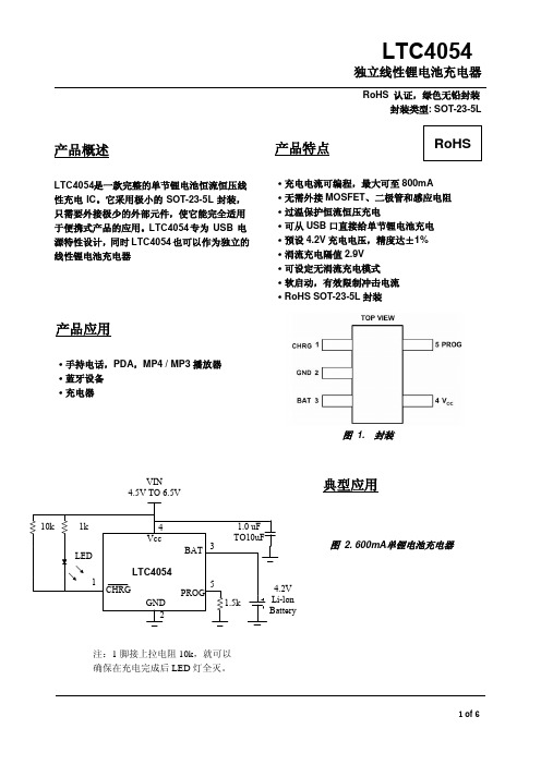
LTC4054
通过热反馈减小充电电流的条件可以近似地估算芯片的耗散功率。几乎所有的功率损耗均是由内部 MOSFET 产生的,有如下近似计算公式:
= PD (VCC −VBAT )IBAT
热保护时芯片周围温度为:
TA = 120°C − PDθJA = 120°C − (VCC −VBAT )I θ BAT JA
产品应用
·充电电流可编程,最大可至 800mA ·无需外接 MOSFET、二极管和感应电阻 ·过温保护恒流恒压充电 ·可从 USB 口直接给单节锂电池充电 ·预设 4.2V 充电电压,精度达±1% ·涓流充电隔值 2.9V ·可设定无涓流充电模式 ·软启动,有效限制冲击电流 ·RoHS SOT-23-5L 封装
充电电流编程脚
CHRG(1):开漏极充电状态输出脚。当对电池充电时,内部 NMOS 管高阻态,LED 灭。
GND(2):电源地。 BAT(3):充电电流输出脚。向电池提供充电电流,同时控制充电完成电压为 4.2V。内部精确电阻分压
0.35
V
二次充电隔值电压
△VRECHRG VFLOAT - VRECHRG
200
mV
恒温下结温
T LIM
120
°C
软启动时间
tSS
IBAT =0至1000V/RPROG
115
μs
二次充电比较器的滤波 器滞后时间 终止充电比较器的滤波 器滞后时间
tRECHRG VBAT由高到低 IBAT降至ICHRG /10
3.9
单位
V
μA
V
mA mA μA μA μA mA V V
电压低压关断滞后电压
V UVHYS
250
mV
PROG脚电压上升时
LTC4413中文资料

DESCRIPTIO
The LTC®4413 contains two monolithic ideal diodes, each capable of supplying up to 2.6A from input voltages between 2.5V and 5.5V. Each ideal diode uses a 100mΩ P-channel MOSFET that independently connects INA to OUTA and INB to OUTB. During normal forward operation the voltage drop across each of these diodes is regulated to as low as 28mV. Quiescent current is less than 40µA for diode currents up to 1A. If either of the output voltages exceeds its respective input voltages, that MOSFET is turned off and less than 1µA of reverse current will flow from OUT to IN. Maximum forward current in each MOSFET is limited to a constant 2.6A and internal thermal limiting circuits protect the part during fault conditions.
LTC4213 1 4213f 电子电路保护器说明书

2µs/DIV4213 TA01b124213fBias Supply Voltage (V CC )...........................–0.3V to 9V Input VoltagesON, SENSEP, SENSEN.............................–0.3V to 9V I SEL ..........................................–0.3V to (V CC + 0.3V)Output VoltagesGATE .....................................................–0.3V to 15V READY.....................................................–0.3V to 9V Operating Temperature RangeLTC4213C ...............................................0°C to 70°C LTC4213I.............................................–40°C to 85°C Storage Temperature Range.................–65°C to 150°C Lead Temperature (Soldering, 10sec)...................300°CORDER PART NUMBER DDB PART*MARKING T JMAX = 125°C, θJA = 250°C/WEXPOSED PAD (PIN 9)PCB CONNECTION OPTIONALConsult LTC Marketing for parts specified with wider operating temperature ranges.*The temperature grade is identified by a label on the shipping container.LBHVLTC4213CDDB LTC4213IDDB ABSOLUTE AXI U RATI GSW W WU PACKAGE/ORDER I FOR ATIOUUW (Note 1)ELECTRICAL CHARACTERISTICSThe ● denotes the specifications which apply over the full operatingtemperature range, otherwise specifications are at T A = 25°C. V CC = 5V, I SEL = 0 unless otherwise noted. (Note 2)SYMBOL PARAMETER CONDITIONSMIN TYP MAX UNITSV CC Bias Supply Voltage ● 2.36V V SENSEP SENSEP Voltage ●06V I CC V CC Supply Current●1.63mA V CC(UVLR)V CC Undervoltage Lockout Release V CC Rising● 1.8 2.07 2.23V ∆V CC(UVHYST)V CC Undervoltage Lockout Hysteresis ●30100160mV I SENSEP SENSEP Input Current V SENSEP = V SENSEN = 5V, Normal Mode 154080µA V SENSEP = V SENSEN = 0, Normal Mode –1±15µA I SENSENSENSEN Input CurrentV SENSEP = V SENSEN = 5V, Normal Mode 154080µA V SENSEP = V SENSEN = 0, Normal Mode –1±15µA V SENSEP = V SENSEN = 5V,50280µAReset Mode or Fault ModeV CBCircuit Breaker Trip Voltage I SEL = 0, V SENSEP = V CC●22.52527.5mV V CB = V SENSEP – V SENSEN I SEL = Floated, V SENSEP = V CC ●455055mV I SEL = V CC, V SENSEP = V CC ●90100110mV V CB(FAST)Fast Circuit Breaker Trip Voltage I SEL = 0, V SENSEP = V CC●63100115mV V CB(FAST)= V SENSEP – V SENSEN I SEL = Floated, V SENSEP = V CC ●126175200mV I SEL = V CC, V SENSEP = V CC ●252325371mV I GATE(UP)GATE Pin Pull Up Current V GATE = 0V●–50–100–150µA I GATE(DN)GATE Pin Pull Down Current ∆V SENSEP – V SENSEN = 200mV, V GATE = 8V ●1040mA ∆V GSMAX External N-Channel Gate Drive V SENSEN = 0, V CC ≥ 2.97V, I GATE = –1µA ● 4.8 6.58V V SENSEN = 0, V CC = 2.3V, I GATE = –1µA ● 2.65 4.38V ∆V GSARMV GS Voltage to Arm Circuit BreakerV SENSEN = 0, V CC ≥ 2.97V ● 4.4 5.47.6V V SENSEN = 0, V CC = 2.3V●2.53.57VTOP VIEWDDB PACKAGE8-LEAD (3mm × 2mm) PLASTIC DFN567894321READY ON I SEL GND V CC SENSEP SENSEN GATE34213f∆V GSMAX – ∆V GSARM Difference Between ∆V GSMAX and V SENSEN = 0, V CC ≥ 2.97V ●0.3 1.1V ∆V GSARMV SENSEN = 0, V CC = 2.3V●0.150.8VV READY(OL)READY Pin Output Low Voltage I READY = 1.6mA, Pull Down Device On ●0.20.4V I READY(LEAK)READY Pin Leakage Current V READY = 5V, Pull Down Device Off ●0±1µA V ON(TH)ON Pin High Threshold ON Rising, GATE Pulls Up ●0.760.80.84V ∆V ON(HYST)ON Pin Hysteresis ON Falling, GATE Pulls Down104090mV V ON(RST)ON Pin Reset Threshold ON Falling, Fault Reset, GATE Pull Down ●0.360.40.44V I ON(IN)ON Pin Input Current V ON = 1.2V●0±1µA ∆V OV Overvoltage Threshold ●0.410.7 1.1V ∆V OV = V SENSEP – V CCt OVOvervoltage Protection Trip Time V SENSEP = V SENSEN = Step 5V to 6.2V 2565160µs t FAULT(SLOW)V CB Trips to GATE Discharging ∆V SENSE Step 0mV to 50mV,●71627µs V SENSEN Falling, V CC = V SENSEP = 5V t FAULT(FAST)V CB(FAST) Trips to GATE Discharging ∆V SENSE Step 0V to 0.3V, V SENSEN Falling,●12.5µs V SENSEP = 5Vt DEBOUNCE Startup De-Bounce Time V ON = 0V to 2V Step to Gate Rising,2760130µs (Exiting Reset Mode)t READY READY Delay Time V GATE = 0V to 8V Step to READY Rising,2250115µs V SENSEP = V SENSEN = 0t OFF Turn-Off Time V ON = 2V to 0.6V Step to GATE Discharging 1.5510µs t ON Turn-On Time V ON = 0.6V to 2V Step to GATE Rising,4816µs (Normal Mode)t RESETReset TimeV ON Step 2V to 0V2080150µsNote 1: Absolute Maximum Ratings are those values beyond which the life of a device may be impaired.ELECTRICAL CHARACTERISTICSThe ● denotes the specifications which apply over the full operatingtemperature range, otherwise specifications are at T A = 25°C. V CC = 5V, I SEL = 0 unless otherwise noted. (Note 2)SYMBOLPARAMETERCONDITIONSMIN TYP MAX UNITSNote 2: All currents into device pins are positive; all currents out of device pins are negative. All voltages are referenced to ground unless otherwise specified.4564213ft RESET vs Temperaturet FAULT(SLOW) vs V CCt FAULT(SLOW) vs Temperaturet FAULT(FAST) vs V CCt FAULT(FAST) vs TemperatureTYPICAL PERFOR A CE CHARACTERISTICSU WSpecifications are at T A = 25°C. V CC = 5Vunless otherwise noted.t F A U L T (F A S T ) (µs )4213 G230.90.80.71.01.11.21.3TEMPERATURE (°C)–50050100125–252575BIAS SUPPLY VOLTAGE (V)2.010t F A U L T (S L O W ) (µs )14121618 3.0 4.0 5.0 6.04213 G202022 2.53.54.55.5TEMPERATURE (°C)–500501001254213 G21–25257510t F A U L T (S L O W ) (µs )141216182022TEMPERATURE (°C)–500501001254213 G19–252575t R E S E T (µs )60708090100BIAS SUPPLY VOLTAGE (V)2.0t F A U L T (F A S T ) (µs )3.04.05.06.04213 G222.53.54.55.50.90.80.71.01.11.21.374213fPI FU CTIO SU U UREADY (Pin 1): READY Status Output. Open drain output that goes high impedance when the external MOSFET is on and the circuit breaker is armed. Otherwise this pin pulls low.ON (Pin 2): ON Control Input. The LTC4213 is in reset mode when the ON pin is below 0.4V. When the ON pin increases above 0.8V, the device starts up and the GATE pulls up with a 100µA current source. When the ON pin drops below 0.76V, the GATE pulls down. To reset a circuit breaker fault, the ON pin must go below 0.4V.I SEL (Pin 3): Threshold Select Input. With the I SEL pin grounded, float or tied to V CC the V CB is set to 25mV, 50mV or 100mV, respectively. The corresponding V CB(FAST)values are 100mV, 175mV and 325mV.GND (Pin 4): Device Ground.GATE (P in 5): GATE D rive Output. An internal charge pump supplies 100µA pull-up current to the gate of the external N-channel MOSFET. Internal circuitry limits thevoltage between the GATE and SENSEN pins to a safe gate drive voltage of less than 8V. When the circuit breaker trips, the GATE pin abruptly pulls to GND.SENSEN (Pin 6): Circuit Breaker Negative Sense Input.Connect this pin to the source of the external MOSFET.During reset or fault mode, the SENSEN pin discharges the output to ground with 280µA.SENSEP (P in 7): Circuit Breaker Positive Sense Input.Connect this pin to the drain of external N-channel MOSFET.The circuit breaker trips when the voltage across SENSEP and SENSEN exceeds V CB . The input common mode range of the circuit breaker is from ground to V CC + 0.2V when V CC < 2.5V. For V CC ≥ 2.5V, the input common mode range is from ground to V CC + 0.4V.V CC (Pin 8): Bias Supply Voltage Input. Normal operation is between 2.3V and 6V. An internal under-voltage lockout circuit disables the device when V CC < 2.07V.Exposed Pad (Pin 9): Exposed pad may be left open or connected to device ground.8910114213fsupply transient dips below 1.97V of less than 80µs are ignored.ON FunctionWhen V ON is below comparator COMP1’s threshold of 0.4V for 80µs, the device resets. The system leaves reset mode if the ON pin rises above comparator COMP2’s threshold of 0.8V and the UVLO condition is met. Leaving reset mode, the GATE pin starts up after a t DEBOUNCE delay of 60µs. When ON goes below 0.76V, the GATE shuts off after a 5µs glitch filter delay. The output is discharged by the external load when V ON is in between 0.4V to 0.8V. At this state, the ON pin can re-enable the GATE if V ON exceeds 0.8V for more than 8µs. Alternatively, the device resets if the ON pin is brought below 0.4V for 80µs. Once reset, the GATE pin restarts only after the t DEBOUNCE 60µs delay at V ON rising above 0.8V. To protect the ON pin from overvoltage stress due to supply transients, a series resistor of greater than 10k is recommended when the ON pin is connected directly to the supply. An external resis-tive divider at the ON pin can be used with COMP2 to set a supply undervoltage lockout value higher than the inter-nal UVLO circuit. An RC filter can be implemented at the ON pin to increase the powerup delay time beyond the internal 60µs delay.Gate FunctionThe GATE pin is held low in reset mode. 60µs after leaving reset mode, the GATE pin is charged up by an internal 100µA current source. The circuit breaker arms when V GATE > V SENSEN + ∆V GSARM . In normal mode operation,the GATE peak voltage is internally clamped to ∆V GSMAX above the SENSEN pin. When the circuit breaker trips, an internal MOSFET shorts the GATE pin to GND, turning off the external MOSFET.READY StatusThe READY pin is held low during reset and at startup. It is pulled high by an external pullup resistor 50µs after the circuit breaker arms. The READY pin pulls low if the circuit breaker trips or the ON pin is pulled below 0.76V, or V CC drops below undervoltage lockout.∆V GSARM and V GSMAXEach MOSFET has a recommended V GS drive voltage where the channel is deemed fully enhanced and R DSON is minimized. Driving beyond this recommended V GS volt-age yields a marginal decrease in R DSON . At startup, the gate voltage starts at ground potential. The GATE ramps past the MOSFET threshold and the load current begins to flow. When V GS exceeds ∆V GSARM , the circuit breaker is armed and enabled. The chosen MOSFET should have a recommended minimum V GS drive level that is lower than ∆V GSARM . Finally, V GS reaches a maximum at ∆V GSMAX.Trip and Reset Circuit BreakerFigure 2 shows the timing diagram of V GATE and V READY after a fault condition. A tripped circuit breaker can be reset either by cycling the V CC bias supply below UVLO thresh-old or pulling ON below 0.4V for >t RESET . Figure 3 shows the timing diagram for a tripped circuit breaker being reset by the ON pin.Calculating Current LimitThe fault current limit is determined by the R DSON of the MOSFET and the circuit breaker voltage V CB .I V R LIMIT CB DSON=()2The R DSON value depends on the manufacturer’s distribu-tion, V GS and junction temperature. Short Kelvin-sense connections between the MOSFET drain and source to the LTC4213 SENSEP and SENSEN pins are strongly recommended.For a selected MOSFET, the nominal load limit current is given by:I V R LIMIT NOM CB NOM DSON NOM ()()()()=3The minimum load limit current is given by:I V R LIMIT MIN CB MIN DSON MAX ()()()()=4APPLICATIO S I FOR ATIOW UUU1213144213fOperating temperature of 0° to 70°C.R DSON @ 25°C = 100%R DSON @ 0°C = 90%R DSON @ 70°C = 120%MOSFET resistance variation:R DSON(NOM) = 15m • 0.82 = 12.3m ΩR DSON(MAX) = 15m • 1.333 • 0.93 • 1.2 = 15m • 1.488= 22.3m ΩR DSON(MIN) = 15m • 0.667 • 0.80 • 0.90 = 15m • 0.480= 7.2m ΩV CB variation:NOM V CB = 25mV = 100%MIN V CB = 22.5mV = 90%MAX V CB = 27.5mV = 110%The current limits are:I LIMIT(NOM) = 25mV/12.3m Ω = 2.03A I LIMIT(MIN) = 22.5mV/22.3m Ω = 1.01A I LIMIT(MAX) = 27.5mV/7.2m Ω = 3.82AFor proper operation, the minimum current limit must exceed the circuit maximum operating load current with margin. So this system is suitable for operating load current up to 1A. From this calculation, we can start with the general rule for MOSFET R DSON by assuming maxi-mum operating load current is roughly half of the I LIMIT(NOM). Equation 7 shows the rule of thumb.I V R OPMAX CB NOM DSON NOM =()()•()27Note that the R DSON(NOM) is at the LTC4213 nominal operating ∆V GSMAX rather than at typical vendor spec.Table 1 gives the nominal operating ∆V GSMAX at the various operating V CC . From this table users can refer to the MOSFET’s data sheet to obtain the R DSON(NOM) value.Table 1. Nominal Operating ∆V GSMAX for Typical Bias Supply VoltageV CC (V)∆V GSMAX (V)2.3 4.32.5 5.02.7 5.63.0 6.53.37.05.07.06.07.0Load Supply Power-Up after Circuit Breaker Armed Figure 4 shows a normal power-up sequence for the circuit in Figure 1 where the V IN load supply power-up after circuit breaker is armed. V CC is first powered up by an auxiliary bias supply. V CC rises above 2.07V at time point 1. V ON exceeds 0.8V at time point 2. After a 60µs debounce delay, the GATE pin starts ramping up at time point 3. The external MOSFET starts conducting at time point 4. At time point 5, V GATE exceed ∆V GSARM and the circuit breaker is armed. After 50µs (t READY delay), READY pulls high by an external resistor at time point 6. READY signals the V IN load supply module to start its ramp. The load supply begins soft-start ramp at time point 7. The load supply ramp rate must be slow to prevent circuit breaker tripping as in equation (8).∆∆V t I I C IN OPMAX LOADLOAD<−()8Where I OPMAX is the maximum operating current defined by equation 7.For illustration, V CB = 25mV and R DSON = 3.5m Ω at the nominal operating ∆V GSMAX . The maximum operating current is 3.5A (refer to equation 7). Assuming the load can draw a current of 2A at power-up, there is a margin of 1.5A available for C LOAD of 100µF and V IN ramp rate should be <15V/ms. At time point 8, the current through the MOSFET reduces after C LOAD is fully charged.APPLICATIO S I FOR ATIOW UUU1516174213fThe selected MOSFET V GS absolute maximum rating should meet the LTC4213 maximum ∆V GSMAX of 8V.Other MOSFET criteria such as V BDSS , I DMAX , and R DSON should be reviewed. Spikes and ringing above maximum operating voltage should be considered when choosing V BDSS . I DMAX should be greater than the current limit. The maximum operating load current is determined by the R DSON value. See the section on “Calculating Current Limit” for details.Supply RequirementsThe LTC4213 can be powered from a single supply or dual supply system. The load supply is connected to the SENSEP pin and the drain of the external MOSFET. In the single supply case, the V CC pin is connected to the load supply, preferably with an RC filter. With dual supplies,V CC is connected to an auxiliary bias supply V AUX where V AUX voltage should be greater or equal to the load supply voltage. The load supply voltage must be capable of sourcing more current than the circuit breaker limit. If the load supply current limit is below the circuit breaker trip current, the LTC4213 may not react when the output overloads. Furthermore, output overloads may trigger UVLO if the load supply has foldback current limit in a single supply system.V IN Transient and Overvoltage ProtectionInput transient spikes are commonly observed whenever the LTC4213 responds to overload. These spikes can be large in amplitude, especially given that large decoupling capacitors are absent in hot swap environments. These short spikes can be clipped with a transient suppressor of adequate voltage and power rating. In addition, the LTC4213can detect a prolonged overvoltage condition. WhenAPPLICATIO S I FOR ATIOW UUU point 6 should be within the circuit breaker limits. Other-wise, the system fails to start and the circuit breaker trips immediately after arming. In most applications additional external gate capacitance is not required unless C LOAD is large and startup becomes problematic. If an external gate capacitor is employed, its capacitance value should not be excessive unless it is used with a series resistor. This is because a big gate capacitor without resistor slows down the GATE turn off during a fault. An alternative method would be a stepped I SEL pin to allow a higher current limit during startup.In the event of output short circuit or a severe overload, the load supply can collapse during GATE ramp up due to load supply current limit. The chosen MOSFET must withstand this possible brief short circuit condition before time point 6 where the circuit breaker is allowed to trip. Bench short circuit evaluation is a practical verification of a reliable design. To have current limit while powering a MOSFET into short circuit conditions, it is preferred that the load supply sequences to turn on after the circuit breaker is armed as described in an earlier section.Power-Off CycleThe system can be powered off by toggling the ON pin low.When ON is brought below 0.76V for 5µs, the GATE and READY pins are pulled low. The system resets when ON is brought below 0.4V for 80µs.MOSFET SelectionThe LTC4213 is designed to be used with logic (5V) and sub-logic (3V) MOSFETs for V CC potentials above 2.97V with ∆V GSMAX exceeding 4.5V. For a V CC supply range between 2.3V and 2.97V, sub-logic MOSFETs should be used as the minimum ∆V GSMAX is less than 4.5V.1819Information furnished by Linear Technology Corporation is believed to be accurate and reliable.However, no responsibility is assumed for its use. Linear Technology Corporation makes no represen-tation that the interconnection of its circuits as described herein will not infringe on existing patent rights.201630 McCarthy Blvd., Milpitas, CA 95035-7417(408) 432-1900 ● FAX: (408) 434-0507 ● © LINEAR TECHNOLOGY CORPORA TION 2005LT/TP 0405 500 • PRINTED IN USA。
- 1、下载文档前请自行甄别文档内容的完整性,平台不提供额外的编辑、内容补充、找答案等附加服务。
- 2、"仅部分预览"的文档,不可在线预览部分如存在完整性等问题,可反馈申请退款(可完整预览的文档不适用该条件!)。
- 3、如文档侵犯您的权益,请联系客服反馈,我们会尽快为您处理(人工客服工作时间:9:00-18:30)。
1ms/DIV4253A TA01b14253a-adjf234253a-adjfI SEL SEL Input CurrentV SEL = 0V (Sourcing)●102040µA V SEL = V IN●±0.1±10µA V CB Circuit Breaker Current Limit Voltage V CB = (V SENSE – V EE )●455055mV V ACL Analog Current Limit Voltage x%V ACL = (V SENSE – V EE ), SS = Open or 1.4V ●105120138% V CB Circuit Breaker Current Limit Voltage V FCL Fast Current Limit Voltage V FCL = (V SENSE – V EE )●150200300mV V SS SS Voltage After End of SS Timing Cycle ● 1.25 1.4 1.55V I SSSS Pin CurrentUV = UVL = OV = OVL = 4V,●162840µA V SENSE = V EE, V SS = 0V (Sourcing)UV = UVL = OV = OVL = 0V,28mA V SENSE = V EE, V SS = 1V (Sinking)R SS SS Output Impedance50k ΩV OS Analog Current Limit Offset Voltage 10mV V ACL + V OSRatio (V ACL + V OS ) to SS Voltage 0.05V/VV SS I GATEGATE Pin Output CurrentUV = UVL = OV = OVL = 4V, V SENSE = V EE ,●305070µA V GATE = 0V (Sourcing)UV = UVL = OV = OVL = 4V, V SENSE – V EE = 0.15V,17mA V GATE = 3V (Sinking)UV = UVL = OV = OVL = 4V, V SENSE – V EE = 0.3V,190mAV GATE = 1V (Sinking)V GATE External MOSFET Gate Drive V GATE – V EE, I IN = 2mA ●1012V ZV V GATEL Gate Low Threshold (Before Gate Ramp Up)0.5V V GATEH Gate High Threshold V GATEH = V IN – V GATE ,2.8VFor PWRGD1, PWRGD2, PWRGD3 Status V UVHI UV Pin Threshold UV Low to High ● 3.05 3.08 3.11V V UVLO UVL Pin Threshold UVL High to Low ● 3.05 3.08 3.11V V OVHI OV Pin Threshold OV Low to High ● 5.04 5.09 5.14V V OVLO OVL Pin Threshold OVL High to Low ●5.0255.08 5.135V I SENSE SENSE Pin Input CurrentUV = UVL = OV = OVL = 4V, V SENSE = 50mV (Sourcing)●1530µA I INP UV, UVL, OV, OVL Pin Input Current UV = UVL = OV = OVL = 4V●±0.1±1µA V TMRH TIMER Pin Voltage High Threshold ● 3.54 4.5V V TMRL TIMER Pin Voltage Low Threshold ●0.81 1.2V I TMRTIMER Pin CurrentTimer On (Initial Cycle/Latchoff, Sourcing), V TMR = 2V ●357µA Timer Off (Initial Cycle, Sinking), V TMR = 2V 28mA Timer On (Circuit Breaker, Sourcing,●120200280µA I DRN = 0µA), V TMR = 2VTimer On (Circuit Breaker, Sourcing,600µAI DRN = 50µA), V TMR = 2VTimer Off (Circuit Breaker, Sinking), V TMR = 2V●357µA ∆I TMRACC (I TMR at I DRN = 50µA – I TMR at I DRN = 0µA)Timer On (Circuit Breaker with I DRN = 50µA)●789µA/µA∆I DRN 50µA V SQTMRH SQTIMER Pin Voltage High Threshold ● 3.54 4.5V V SQTMRLSQTIMER Pin Voltage Low Threshold0.33VSYMBOL PARAMETER CONDITIONS MIN TYP MAX UNITS ELECTRICAL CHARACTERISTICSThe ● denotes the specifications which apply over the full operatingtemperature range, otherwise specifications are at T A = 25°C. (Note 2)456784253a-adjfEN2 (Pin 1/Pin 18): Power Good Status Output Two Enable. This is a TTL compatible input that is used to control PWRGD 2 and PWRGD 3 outputs. When EN2 is driven low, both PWRGD 2 and PWRGD 3 will go high.When EN2 is driven high, PWRGD2 will go low provided PWRGD1 has been active for more than one power good sequence delay (t SQT ) provided by the sequencing timer.EN2 can be used to control the power good sequence. This pin is internally pulled low by a 120µA current source.PWRGD2 (Pin 2/Pin 19): Power Good Status Output Two.Power good sequence starts with D RAIN going below 2.39V and GATE is within 2.8V on V IN . PWRGD2 will latch active low after EN2 goes high and after one power good sequence delay t SQT provided by the sequencing timer from the time PWRGD1 goes low, whichever comes later.PWRGD2 is reset by PWRGD1 going high or EN2 going low. This pin is internally pulled high by a 50µA current source.PWRGD1 (Pin 3/Pin 20): Power Good Status Output One.At start-up, PWRGD1 latches active low one t SQT after both DRAIN is below 2.39V and GATE is within 2.8V of V IN .PWRGD1 status is reset by undervoltage, V IN (UVLO),RESET going high or circuit breaker fault time-out. This pin is internally pulled high by a 50µA current source.V IN (Pin 4/Pin 1): Positive Supply Input. Connect this pin to the positive side of the supply through a dropping resistor. A shunt regulator clamps V IN at 13V above V EE .An internal undervoltage lockout (UVLO) circuit holds GATE low until the V IN pin is greater than V LKO (9V),overriding undervoltage and overvoltage events. If there is no undervoltage, no overvoltage and V IN comes out of UVLO, TIMER starts an initial timing cycle before initiating GATE ramp up. If V IN drops below approximately 8.5V,GATE pulls low immediately.RESET (Pin 5/Pin 2): Circuit Breaker Reset Pin. This is an asynchronous TTL compatible input. RESET going high will pull GATE, SS, TIMER, SQTIMER low and the PWRGD outputs high. The RESET pin has an internal glitch filter that rejects any pulse < 20µs. After the reset of a latched fault, the chip waits for the interlock conditions before recovering as described in Interlock Conditions in the Operation section.SS (Pin 6/Pin 3): Soft-Start Pin. This pin is used to ramp inrush current during start up, thereby effecting control over di/dt. A 20X attenuated version of the SS pin voltage is presented to the current limit amplifier. This attenuated voltage limits the MOSFET’s drain current through the sense resistor during the soft-start current limiting. At the beginning of the start-up cycle, the SS capacitor (C SS ) is ramped by a 28µA current source. The GATE pin is held low until SS exceeds 20 • V OS = 0.2V. SS is internally shunted by a 50k R SS which limits the SS pin voltage to 1.4V. This corresponds to an analog current limit SENSE voltage of 60mV.SEL (Pin 7/Pin 4): Soft-Start Mode Select. This is an asynchronous TTL compatible input. SEL has an internal pull-up of 20µA that will pull it high if it is floated. SEL selects between two modes of SS ramp-up (see Applica-tions Information, Soft-Start section).SENSE (Pin 8/Pin 5): Circuit Breaker/Current Limit Sense Pin. Load current is monitored by a sense resistor R S connected between SENSE and V EE , and controlled in three steps. If SENSE exceeds V CB (50mV), the circuit breaker comparator activates a (200µA +8•I DRN ) TIMER pull-up current. If SENSE exceeds V ACL (60mV), the analog current-limit amplifier pulls GATE down to regulate the MOSFET current at V ACL /R S . In the event of a cata-strophic short-circuit, SENSE may overshoot V ACL . If SENSE reaches V FCL (200mV), the fast current-limit com-parator pulls GATE low with a strong pull-down. To disable the circuit breaker and current limit functions, connect SENSE to V EE .V EE (Pins 9, 10/Pin 7): Negative Supply Voltage Input.Connect this pin to the negative side of the power supply.GATE (Pin 11/Pin 8): N-channel MOSFET Gate D rive Output. This pin is pulled high by a 50µA current source.GATE is pulled low by invalid conditions at V IN (UVLO),undervoltage, overvoltage, during the initial timing cycle,a circuit breaker fault time-out or the RESET pin going high. GATE is actively servoed to control the fault current as measured at SENSE. Compensation capacitor, C C , at GATE stabilizes this loop. A comparator monitors GATE to ensure that it is low before allowing an initial timing cycle,then the GATE ramps up after an overvoltage event orPI FU CTIO SU U U(SSOP/QFN)94253a-adjfrestart after a current limit fault. During GATE start-up, a second comparator detects GATE within 2.8V of V IN before power good sequencing starts.DRAIN (Pin 12/Pin 9): Drain Sense Input. Connecting an external resistor, R D between this pin and the MOSFET’s drain (V OUT ) allows voltage sensing below 5V and current feedback to TIMER. A comparator detects if D RAIN is below 2.39V and together with the GATE high comparator,starts the power good sequencing. If V OUT is above V DRNCL , the D RAIN pin is clamped at approximately V DRNCL .R D current is internally multiplied by 8 and added to TIMER’s 200µA during a circuit breaker fault cycle. This reduces the fault time and MOSFET heating.OV/OVL (Pins 13, 14/Pins 10, 11): Overvoltage and Overvoltage Low Inputs. The OV and OVL pins work together to implement the overvoltage function. OVL and OV must be tapped from an external resistive string across the input supply such that V OVL ≥ V OV under all circum-stances. As the input supply ramps up, the OV pin input is multiplexed to the internal overvoltage comparator input.If OV > 5.09V, GATE pulls low and the overvoltage com-parator input is switched to OVL. When OVL returns below 5.08V, GATE start-up begins without an initial timing cycle and the overvoltage comparator input is switched to OV.In this way, an external resistor between OVL and OV can set a low to high and high to low overvoltage threshold hysteresis that will add to the internal 10mV hysteresis. A 1nF to 10nF capacitor at OVL prevents transients and switching noise at both OVL and OV from causing glitches at the GATE.UV/UVL (Pins 15, 16/Pins 12, 13): Undervoltage and Undervoltage Low Inputs. The UV and UVL pins work together to implement the undervoltage function. UVL and UV must be tapped from an external resistive string across the input supply such that V UVL ≥ V UV under all circum-stances. As the input supply ramps up, the UV pin input is multiplexed to the internal undervoltage comparator in-put. If UV > 3.08V, an initial timing cycle is initiatedfollowed by GATE start-up and input to the undervoltage comparator input is switched to UVL. When UVL returns below 3.08V, PWRGD1 pulls high, both GATE and TIMER pull low and input to the undervoltage comparator input is switched to UV. In this way, an external resistor between UVL and UV can set the low to high and high to low undervoltage threshold hysteresis. A 1nF to 10nF capaci-tor at UVL prevents transients and switching noise at both UVL and UV from causing glitches at the GATE pin.TIMER (Pin 17/Pin 14): Timer Input. Timer is used to generate an initial timing delay at start-up, and to delay shutdown in the event of an output overload (circuit breaker fault). These delays are adjustable by connecting an appropriate capacitor to this pin.SQTIMER (Pin 18/Pin 15): Sequencing Timer Input. The sequencing timer provides a delay t SQT for the power good sequencing. This delay is adjusted by connecting an appropriate capacitor to this pin. If the SQTIMER capacitor is omitted, the SQTIMER pin ramps from 0V to 4V in about 300µs.EN3 (Pin 19/Pin 16): Power Good Status Output Three Enable. This is a TTL compatible input that is used to control the PWRGD3 output. When EN3 is driven low,PWRGD3 will go high. When EN3 is driven high, PWRGD3will go low provided PWRGD2 has been active for for more than one power good sequence delay (t SQT ). EN3 can be used to control the power good sequence. This pin is internally pulled low by a 120µA current source.PWRGD3 (Pin 20/Pin 17): Power Good Status Output Three. Power good sequence starts with D RAIN going below 2.39V and GATE is within 2.8V of V IN . PWRGD3 will latch active low after EN3 goes high and after one power good sequence delay t SQT provided by the sequencing timer from the time PWRGD2 goes low, whichever comes later. PWRGD3 is reset by PWRGD1 going high or EN3going low. This pin is internally pulled high by a 50µA current source.PI FU CTIO SU U U(SSOP/QFN)1011OPERATIOIf RESET < 0.8V occurs after the LTC4253A-ADJ comes out of UVLO (interlock condition 1) and undervoltage (interlock condition 2), GATE and SS are released without an initial TIMER cycle once the other interlock conditions are met (see Figure 13a). If not, TIMER begins the start-up sequence by sourcing 5µA into C T. If V IN, UVL/UV or OVL/ OV falls out of range or RESET asserts, the start-up cycle stops and TIMER discharges C T to less than 1V, then waits until the aforementioned conditions are once again met. If C T successfully charges to 4V, TIMER pulls low and both SS and GATE pins are released. GATE sources 50µA (I GATE), charging the MOSFET gate and associated capaci-tance. The SS voltage ramp limits V SENSE to control the inrush current. The SEL pin selects between two different modes of SS ramp-up (refer to Applications Information, Soft-Start section). SQTIMER starts its ramp-up when GATE is within 2.8V of V IN and DRAIN is lower than V DRNL. This sets off the power good sequence in which PWRGD1, PWRGD2 and then PWRGD3 is subsequently pulled low after a delay, adjustable through the SQTIMER capacitor C SQ or by external control inputs EN2 and EN3. In this way, external loads or power modules controlled by the three PWRGD signals are turned on in a controlled manner without overloading the power bus.Two modes of operation are possible during the time the MOSFET is first turned on, depending on the values of external components, MOSFET characteristics and nomi-nal design current. One possibility is that the MOSFET will turn on gradually so that the inrush into the load capacitance remains a low value. The output will simply ramp to –48V and the LTC4253A-ADJ will fully enhance the MOSFET. A second possibility is that the load current exceeds the soft-start current limit threshold of [V SS(t)/20 – V OS]/R S. In this case the LTC4253A-ADJ will ramp the output by sourcing soft-start limited current into the load capacitance. If the soft-start voltage is below 1.2V, the circuit breaker TIMER is held low. Above 1.2V, TIMER ramps up. It is important to set the timer delay so that, regardless of which start-up mode is used, the TIMER ramp is less than one circuit breaker delay time. If this condition is not met, the LTC4253A-ADJ may shut down after one circuit breaker delay time.Board RemovalWhen the board is withdrawn from the card cage, the UVL/ UV/OVL/OV divider is the first to lose connection. This shuts off the MOSFET and commutates the flow of current in the connector. When the power pins subsequently separate there is no arcing.Current ControlThree levels of protection handle short-circuit and over-load conditions. Load current is monitored by SENSE and resistor R S. There are three distinct thresholds at SENSE: 50mV for a timed circuit breaker function; 60mV for an analog current limit loop; and 200mV for a fast, feedforward comparator which limits peak current in the event of a catastrophic short-circuit.If, due to an output overload, the voltage drop across R S exceeds 50mV, TIMER sources 200µA into C T. C T eventu-ally charges to a 4V threshold and the LTC4253A-ADJ shuts off. If the overload goes away before C T reaches 4V and SENSE measures less than 50mV, C T slowly dis-charges (5µA). In this way the LTC4253A-ADJ’s circuit breaker function responds to low duty cycle overloads, and accounts for the fast heating and slow cooling char-acteristic of the MOSFET.Higher overloads are handled by an analog current limit loop. If the drop across R S reaches V ACL, the current limiting loop servos the MOSFET gate and maintains a constant output current of V ACL/R S. In current limit mode, V OUT (MOSFET drain-source voltage drop) typically rises and this increases MOSFET heating. If V OUT > V DRNCL, connecting an external resistor, R D between V OUT and DRAIN allows the fault timing cycle to be shortened by accelerating the charging of the TIMER capacitor. The TIMER pull-up current is increased by 8 • I DRN. Note that because SENSE > 50mV, TIMER charges C T during this time, and the LTC4253A-ADJ will eventually shut down. L ow impedance failures on the load side of the LTC4253A-AD J coupled with 48V or more driving potential can produce current slew rates well in excess of 50A/µs. Under these conditions, overshoot is inevitable. A fast SENSE124253a-adjfOPERATIOcomparator with a threshold of 200mV detects overshoot and pulls GATE low much harder and hence much faster than the weaker current limit loop. The V ACL/R S current limit loop then takes over, and servos the current as previously described. As before, TIMER runs and shuts down LTC4253A-ADJ when C T reaches 4V.If C T reaches 4V, the LTC4253A-ADJ latches off with a 5µA pull-up current source. The LTC4253A-ADJ circuit breaker latch is reset by either pulling the RESET pin active high for >20µs, pulling UVL/UV momentarily low, dropping the input voltage V IN below the internal UVLO threshold or pulsing TIMER momentarily low with a switch.Although short-circuits are the most obvious fault type, several operating conditions may invoke overcurrent protection. Noise spikes from the backplane or load, input steps caused by the connection of a second, higher voltage supply, transient currents caused by faults on adjacent circuit boards sharing the same power bus or the insertion of non-hot swappable products could cause higher than anticipated input current and temporary de-tection of an overcurrent condition. The action of TIMER and C T rejects these events allowing the LTC4253A-ADJ to “ride out” temporary overloads and disturbances that could trip a simple current comparator and, in some cases, blow a fuse.134253a-adjf14154253a-adjfAPPLICATIO S I FOR ATIOW UUU Figure 2b shows the implementation of the overvoltage function of the Typical Application. During UVLO, OVD is forced high so OVL is multiplexed to OVIN. At time point 1, the part exits UVLO and the overvoltage comparator is enabled. OVIN = OVL is less than V OVLO (5.08V) so OVD goes low, switching OV to OVIN and bringing the part to Normal mode. At time point 2, OV ramps past V OVHI (5.09V) and OVD goes high, switching OVL to OVIN as well as turning on the internal 10mV hysteresis as the part goes into overvoltage. OVL is tied to OVIN until time point 3when OVL ramps past V OVLO (5.09V – 10mV = 5.08V) and OVD goes low, bringing the part into Normal mode and switching OV to OVIN.The undervoltage (UV) comparator has no internal hyster-esis to preserve the accuracy of the hysteresis set across UVL/UV while the overvoltage (OV) comparator has an internal low to high hysteresis of 10mV. This will add to the hysteresis set across OVL/OV and provide some noise immunity if OVL/OV is shorted together. Any implementa-tion must ensure that V UVL ≥ V UV and V OVL ≥ V OV under all conditions.The various thresholds to note are:UV low-to-high (V UVHI ) = 3.08V UVL high-to-low (V UVLO ) = 3.08V OV low-to-high (V OVHI ) = 5.09V OVL high-to-low (V OVLO ) = 5.08VUsing these thresholds and an external resistive divider,any required supply operating range can be implemented.An example is shown in Figure 1 where the required typical operating range is:Undervoltage low-to-high (V 48UVHI ) = 43V Undervoltage high-to-low (V 48UVLO ) = 39V Overvoltage low-to-high (V 48OVHI ) = 82V Overvoltage high-to-low (V 48OVLO ) = 78VA quick check of the resistive divider ratios required at UVL, UV, OVL and OV confirms that UVL is tapped between R5/R4, UV is tapped between R4/R3, OVL is tapped between R3/R2 and OV is tapped between R2/R1.From Figure 1, by looking at the voltages at OV, OVL, UV and UVL, the following equations are obtained:R R V V where R R R R R R R R V V TOTAL OVHIOVHI TOTAL TOTAL OVHIOVHI11234514848==++++()=:•(1a)R R R V V R R V V VV R TOTAL OVLOOVLOOVLO OVLO OVHI OVHI 12211484848+==⎛⎝⎜⎞⎠⎟•–(1b)R R R R VV R R V V VV R R TOTAL UVHIUVHIUVHI UVHI OVHI OVHI 1233112484848++==⎛⎝⎜⎞⎠⎟•––(1c)R R R R R VV R R V V VV R R R TOTAL UVLOUVLOUVLO UVLO OVHI OVHI 123441123484848+++==⎛⎝⎜⎞⎠⎟•–––(1d)Starting with a value of 20k for R1, Equation 1b gives R2= 0.984k (use closest 1% standard value of 0.976k). Using R1 = 20k and R2 = 0.976k, Equation 1c gives R3 = 2.103k (use the closest 1% standard value of 2.1k). Using R1 =20k, R2 = 0.976k and R3 = 2.1k, Equation 1d gives R4 =2.37k (use closest 1% standard value of 2.37k). Using R1= 20k, R2 = 0.976k, R3 = 2.1k and R4 = 2.37k in Equation 1a, R5 = 296.754k (use 1% standard values of 294k in series with 2.74k).The divider values shown set a standing current of slightly more than 150µA and define an impedance at UVL/UV/OVL/OV of approximately 20k. This impedance will work with the hysteresis set across UVL/UV and OVL/OV to provide noise immunity to the UV and OV comparators. If164253a-adjfAPPLICATIO S I FOR ATIOW UUU more noise immunity is desired, add a 1nF to 10nF filter capacitor from UVL to V EE .UV/OV OPERATIONAn undervoltage condition detected by the UV comparator immediately shuts down the LTC4253A-ADJ, pulls GATE,SS and TIMER low and resets the three latched PWRGD signals high. Recovery from an undervoltage will initiate an initial timing sequence if the other interlock conditions are met.An overvoltage condition is detected by the OV compara-tor and pulls GATE low, thereby shutting down the load,but it will not reset the circuit breaker TIMER and PWRGD flags. Returning from the overvoltage condition will restart the GATE pin if all the interlock conditions except TIMER are met. Only during the initial timing cycle does an overvoltage condition have an effect of resetting TIMER.The internal UVLO at V IN always overrides an overvoltage or undervoltage.DRAINConnecting an external resistor, R D , to this dual function DRAIN pin allows V OUT (MOSFET drain-source voltage drop) sensing without it being damaged by large voltage transients. Below 5V, negligible pin leakage allows a DRAIN low comparator to detect V OUT less than 2.39V (V DRNL ). This, together with the GATE low comparator,starts the power good sequencing.When V OUT > V DRNCL , the DRAIN pin is clamped at V DRNCL and the current flowing in R D is given by:I V V R DRN OUT DRNCLD≈−(2)This current is scaled up 8 times during a circuit breaker fault before being added to the nominal 200µA. This accelerates the fault TIMER pull-up when the MOSFET’s drain-source voltage exceeds V DRNCL and effectively short-ens the MOSFET heating duration.TIMERThe operation of the TIMER pin is somewhat complex as it handles several key functions. A capacitor C T is used atTIMER to provide timing for the LTC4253A-AD J. Four different charging and discharging modes are available at TIMER:1. 5µA slow charge; initial timing delay.2. (200µA +8•I DRN ) fast charge; circuit breaker delay.3. 5µA slow discharge; circuit breaker “cool-off.”4. Low impedance switch; resets the TIMER capacitor after an initial timing delay, in UVLO, in UV and in OV during initial timing and when RESET is high.For initial timing delay, the 5µA pull-up is used. The low impedance switch is turned off and the 5µA current source is enabled when the interlock conditions are met. C T charges to 4V in a time period given by:t V C AT =µ45•(3)When C T reaches V TMRH (4V), the low impedance switch turns on and discharges C T . A GATE start-up cycle begins and both SS and GATE outputs are released.CIRCUIT BREAKER TIMER OPERATIONI f the SENSE pin detects more than 50mV drop across R S , the TIMER pin charges C T with (200µA +8•I DRN ). If C T charges to 4V, the GATE pin pulls low and the LTC4253A-ADJ latches off. The LTC4253A-ADJ remains latched off until the RESET pin is momentarily pulsed high, the UVL/UV pin is momentarily pulsed low, the TIMER pin is momentarily discharged low by an external switch or V IN dips below UVLO and is then restored. The circuit breaker timeout period is given by:t V C A I TDRN=µ+42008••(4)If V OUT < 5V, an internal PMOS isolates DRAIN pin leakage current and this makes I DRN = 0 in Equation 4. If V OUT is above V DRNCL during the circuit breaker fault period, the charging of C T is accelerated by 8 • I DRN of Equation 2.Intermittent overloads may exceed the 50mV threshold at SENSE but, if their duration is sufficiently short, TIMER will not reach 4V and the LTC4253A-ADJ will not shut the17184253a-adjfAPPLICATIO S I FOR ATIOW UUU When V ACL (t) exceeds V SENSE , the ACL amplifier exits current limit mode and releases its pull-down on GATE. V SS (t) = 20 • (V OS + V SENSE ) from Equation 7. So when V SS (t)> 20 • V OS = 0.2V (since V SENSE = 0V), GATE starts to ramp up and SS continues to ramp up. When GATE clears the threshold of the external FET and inrush current starts flow-ing, V ACL (t) = (V SS (t)/20 – V OS ) will have a positive offset from zero. V SENSE will show an initial jump to clear this offset before going into analog current limit (Figure 4a).If SEL is set low during SS ramp-up, V SS is servoed when it exceeds 20 • V OS = 0.2V and GATE starts its ramp-up.V SS is servoed at a voltage that is just above 20 • V OS to keep the ACL amplifier off and GATE ramping up freely. Once GATE clears the threshold of the external FET, inrush cur-rent starts flowing and V SENSE will jump above V ACL (t). This will engage the ACL amplifier and mask off V SS servo so V SS continues its RC ramp-up. In this way, the LTC4253A-ADJ enters analog current limit with V ACL (t) =(V SS (t)/20 – V OS ) ramping up from close to zero. The resultant inrush current profile presents a smooth ramp up from zero (Figure 4b). If there is little inrush current so the LTC4253A-ADJ does not enter current limit, V SS servo will be masked off when DRAIN goes below 2.39V (V DRNL ) and latched off when GATE goes within 2.8V of V IN (V GATEH ).A minimum C SS of 5nF is required for the stability of the V SS servo loop.SS is discharged low during UVLO, UV, OV, during the initial timing cycle, a latched circuit breaker fault or the RESET pin going high.GATEGATE is pulled low to V EE under any of the following conditions: in UVLO, when RESET pulls high, in an undervoltage condition, in an overvoltage condition, dur-ing the initial timing cycle or a latched circuit breaker fault.When GATE turns on, a 50µA current source charges the MOSFET gate and any associated external capacitance.V IN limits the gate drive to no more than 14.5V.Gate-drain capacitance (C GD ) feedthrough at the first abrupt application of power can cause a gate-source voltage sufficient to turn on the MOSFET. A unique circuit pulls GATE low with practically no usable voltage at V IN ,and eliminates current spikes at insertion. A large external gate-source capacitor is thus unnecessary for the purpose of compensating C GD . Instead, a smaller value (≥10nF)capacitor C C is adequate. C C also provides compensation for the analog current limit loop.GATE has two comparators: the GATE low comparator looks for <0.5V threshold prior to initial timing; the GATE high comparator looks for <2.8V relative to V IN and,together with DRAIN low comparator, starts power good sequencing during GATE start-up.SENSEThe SENSE pin is monitored by the circuit breaker (CB)comparator, the analog current limit (ACL) amplifier, and the fast current limit (FCL) comparator. Each of these three measures the potential of SENSE relative to V EE . WhenFigure 4. Two Modes of SS Ramp Up(4a) SEL Set High(4b) SEL Set LowGATE 10VSS 1VSENSE 50mVV OUT50V1ms/DIV4253A F04a19Figure 5. Output Short-Circuit Behavior of LTC4253A-ADJ0.5ms/DIV4253A F05C TIMER RAMPANALOG CURRENT LIMITFAST CURRENT LIMIT ONSET OF OUTPUT SHORT CIRCUITSUPPLY RING OWING TO CURRENT OVERSHOOTLATCH OFF204253a-adjfAPPLICATIO S I FOR ATIOW UUU MOSFET selection is a 3-step process by assuming the absense of soft-start capacitor. First, R S is calculated and then the time required to charge the load capacitance is determined. This timing, along with the maximum short-circuit current and maximum input voltage, defines an operating point that is checked against the MOSFET’s SOA curve.To begin a design, first specify the required load current and Ioad capacitance, I L and C L . The circuit breaker current trip point (V CB /R S ) should be set to accommodate the maximum load current. Note that maximum input current to a DC/DC converter is expected at V SUPPLY(MIN).R S is given by:R V I S CB MIN L MAX =()()(9)where V CB(MIN) = 45mV represents the guaranteed mini-mum circuit breaker threshold.During the initial charging process, the LTC4253A-ADJ may operate the MOSFET in current limit, forcing (V ACL )between 54mV to 66mV across R S . The minimum inrush current is given by:I V R INRUSH MIN ACL MIN S()()=(10)Maximum short-circuit current limit is calculated using the maximum V SENSE . This gives I V R SHORTCIRCUIT MAX ACL MAX S()()=(11)The TIMER capacitor, C T , must be selected based on the slowest expected charging rate; otherwise TIMER might time out before the load capacitor is fully charged. A value for C T is calculated based on the maximum time it takes the load capacitor to charge. That time is given by:t C V I C V I CL CHARGE L SUPPLY MAX INRUSH MIN ()()()••==(12)The maximum current flowing in the DRAIN pin is given by:I V V R DRN MAX SUPPLY MAX DRNCLD()()=−(13)Approximating a linear charging rate, I DRN drops from I DRN(MAX) to zero, the I DRN component in Equation 4 can be approximated with 0.5 • I DRN(MAX). Rearranging the equation, TIMER capacitor C T is given by:C t A I VT CL CHARGE DRN MAX =µ+()()•(•)20044(14)Returning to Equation 4, the TIMER period is calculated and used in conjunction with V SUPPLY(MAX) and I SHORTCIRCUIT(MAX) to check the SOA curves of a prospec-tive MOSFET.As a numerical design example, consider a 30W load,which requires 1A input current at 36V. If V SUPPLY(MAX) =72V and C L = 100µF, R D = 1M Ω, Equation 9 gives R S =45m Ω; use R S = 40m Ω for more margin. Equation 14gives C T = 619nF. To account for errors in R S , C T , TIMER current (200µA), TIMER threshold (4V), R D , DRAIN cur-rent multiplier and DRAIN voltage clamp (V DRNCL ), the calculated value should be multiplied by 1.5, giving the nearest standard value of C T =1µF.If a short-circuit occurs, a current of up to 66mV/45m Ω=1.65A will flow in the MOSFET for 9.1ms as dictated by C T = 1µF in Equation 4. The MOSFET must be selected based on this criterion. The IRF530S can handle 100V and 2A for 22.5ms and is safe to use in this application.Computing the maximum soft-start capacitor value during soft-start to a load short is complicated by the nonlinear MOSFET’s SOA characteristics and the R SS C SS response.An overconservative but simple approach begins with the maximum circuit breaker current, given by:I V R CB MAX CB MAX S()()=(15)From the SOA curves of a prospective MOSFET, determine the time allowed, t SOA(MAX). C SS is given by:C t R SS SOA MAX SS=().•248(16)In the above example, 55mV/40m Ω gives 1.375A. t SOA for the IRF530S is 47.6ms. From Equation 16, C SS = 384nF.。