MAX6312UK26D3中文资料
PC-6312 模入模出接口卡技术说明书
4. 安装及使用注意: 本卡的安装十分简便,在关电情况下,将主机机壳打开,将本卡插入主机的任何一个 ISA 空余扩展槽中,再将
4
a. IRQ3 中断
b. IRQ5 中断
c. IRQ7 中断
图 8 中断源的选择
5.5 控制端口地址与有关数据格式:
5.5.1 各个控制端的操作地址与功能见表 2:
表 2 端口地址与功能
端口操作地址 操作命令
功
能
基地址+0
写
写程控增益代码和通道代码,选通道。
基地址+0
读
启动 D/A 转换
基地址+1
的输出方式和范围,互不影响。各组插座的使用方法见图 7。
a. 0~10V
b. 0~5V
c. ±5V
d. ±2.5V
e. ±10V
f. 1~5V
g. 0~10mA
h. 4~20mA
图 7 D/A 输出方式及范围选择
5.4.5 中断方式及中断源选择:
KJ7 为中断有效及中断源选择插座。该插座全部开路时为非中断方式,中断源的选择见图 8。
3
5.4.1 输入单/双端方式选择: KJ1、KJ2 为单/双端输入方式选择,其使用方法见图 4。
KJ2
KJ1
KJ2
KJ1
a. 单端输入方式
b. 双端输入方式
图 4 单/双端输入方式选择
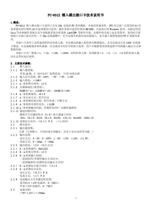
MAX26_系列数字编码式滤波器的使用方法
第32卷第3期2000年5月四川大学学报(工程科学版)J OURNA L OF SICHUAN UNIVERSITY(ENGINEERING SCIENCE EDITIO N)Vol.32No.3May2000文章编号:1009-3087(2000)03-0058-03MAX26系列数字编码式滤波器的使用方法羿飒,田远富(四川大学电气信息学院,成都610065)摘要:主要介绍MAX26系列4阶开关电容滤波器的使用方法。
给出了其引脚图及各引脚功能,指明了其使用的电压频率范围,说明了如何进行模式选择以及在不同模式下频率编码输入端和Q值编码输入端的设定。
总结了其性能优点,特别指出了实际应用中应注意的问题。
并在理论计算的基础上,设计出用MAX267实现中心频率220 Hz,带宽6.875Hz的带通滤波电路,进一步通过实验测试,验证了MAX26系列数字滤波器的滤波效果。
关键词:数字滤波器;中心频率;带宽中图分类号:TN713.92文献标识码:AUsage of MAX26Series Digital FilterY I Sa,TIAN Y uan-f u(College of Electrical Informati on,Sichuan Uni v.,Chengdu610065,Chi na)Abstract:This paper mainly introduces the operation methods of the MAX26series four-order on-off capacitance filter. We provide the pin description,show clearly the applicable range of volt and frequency,demonstrate how to select mode and set up the frequency-encode input and Q value-encode input under each mode,summarize the virtues of properties, especially point out the problems which should be a ware of in actual applications.Then on the basis of theoretic calcula-tion,we have designed the band-pass filter circuit,which can realize center frequenc y220Hz,bandwidth6.875Hz by using MAX267.Through experimental test,take further steps to verify the filter effect of MAX26series digital filter. Key words:digital filter;center frequenc y;bandwidthMAX263/264/267/268是MAXIM公司新推出的4种应用非常广泛的4阶开关电容滤波器。
MAX4233中文资料
General DescriptionThe MAX4230–MAX4234 single/dual/quad, high-output-drive CMOS op amps feature 200mA of peak output current, rail-to-rail input, and output capability from a single 2.7V to 5.5V supply. These amplifiers exhibit a high slew rate of 10V/µs and a gain-bandwidth product (GBWP) of 10MHz. The MAX4230–MAX4234 can drive typical headset levels (32Ω), as well as bias an RF power amplifier (PA) in wireless handset applications.The MAX4230 comes in a tiny 5-pin SC70 package and the MAX4231, single with shutdown, is offered in the 6-pin SC70 package. The dual op-amp MAX4233 is offered in the space-saving 10-bump UCSP™, provid-ing the smallest footprint area for a dual op amp with shutdown.These op amps are designed to be part of the PA con-trol circuitry, biasing RF PAs in wireless headsets. The MAX4231/MAX4233 offer a SHDN feature that drives the output low. This ensures that the RF PA is fully dis-abled when needed, preventing unconverted signals to the RF antenna.The MAX4230 family offers low offsets, wide bandwidth,and high-output drive in a tiny 2.1mm x 2.0mm space-saving SC70 package. These parts are offered over the automotive temperature range (-40°C to +125°C).ApplicationsRF PA Biasing Controls in Handset Applications Portable/Battery-Powered Audio Applications Portable Headphone Speaker Drivers (32Ω)Audio Hands-Free Car Phones (Kits)Laptop/Notebook Computers/TFT Panels Sound Ports/Cards Set-Top BoxesDigital-to-Analog Converter Buffers Transformer/Line Drivers Motor DriversFeatureso 30mA Output Drive Capability o Rail-to-Rail Input and Output o 1.1mA Supply Current per Amplifier o 2.7V to 5.5V Single-Supply Operation o 10MHz Gain-Bandwidth Product o High Slew Rate: 10V/µso 100dB Voltage Gain (R L = 100k Ω)o 85dB Power-Supply Rejection Ratio o No Phase Reversal for Overdriven Inputs o Unity-Gain Stable for Capacitive Loads to 780pF o Low-Power Shutdown Mode Reduces Supply Current to <1µA o Available in 5-Pin SC70 Package (MAX4230)o Available in 10-Bump UCSP Package (MAX4233)MAX4230–MAX4234High-Output-Drive, 10MHz, 10V/µs,Rail-to-Rail I/O Op Amps with Shutdown in SC70________________________________________________________________Maxim Integrated Products 119-2164; Rev 4; 5/04Ordering Information continued at end of data sheet.For pricing, delivery, and ordering information,please contact Maxim/Dallas Direct!at 1-888-629-4642, or visit Maxim’s website at .Selector Guide appears at end of data sheet.Pin Configurations appear at end of data sheet.UCSP is a trademark of Maxim Integrated Products, Inc.Ordering InformationTypical Operating CircuitM A X 4230–M A X 4234High-Output-Drive, 10MHz, 10V/µs,Rail-to-Rail I/O Op Amps with Shutdown in SC702_______________________________________________________________________________________ABSOLUTE MAXIMUM RATINGSStresses beyond those listed under “Absolute Maximum Ratings” may cause permanent damage to the device. These are stress ratings only, and functional operation of the device at these or any other conditions beyond those indicated in the operational sections of the specifications is not implied. Exposure to absolute maximum rating conditions for extended periods may affect device reliability.Supply Voltage (V DD to V SS )....................................................6V All Other Pins....................................(V SS - 0.3V) + (V DD + 0.3V)Output Short-Circuit Duration to V DD or V SS (Note 1)..................1s Continuous Power Dissipation (T A = +70°C)5-Pin SC70 (derate 3.1mW/°C above +70°C)..............247mW 5-Pin SOT23 (derate 7.1mW/°C above +70°C)............571mW 6-Pin SC70 (derate 3.1mW/°C above +70°C)..............245mW 6-Pin SOT23 (derate 8.7mW/°C above +70°C) ...........696mW 8-Pin SOT23 (derate 8.9mW/°C above +70°C) ...........714mW 8-Pin µMAX (derate 4.5mW/°C above +70°C) ............362mW 10-Pin µMAX (derate 5.6mW/°C above +70°C) ..........444mW 10-Bump UCSP (derate 6.1mW/°C above +70°C) .....484mW 14-Pin TSSOP (derate 9.1mW/°C above +70°C) ........727mW 14-Pin SO (derate 8.3mW/°C above +70°C) ...............667mW Operating Temperature Range .........................-40°C to +125°C Junction Temperature......................................................+150°C Storage Temperature Range.............................-65°C to +150°C Lead Temperature (soldering, 10s).................................+300°CNote 1:Package power dissipation should also be observed.DC ELECTRICAL CHARACTERISTICS(V DD = 2.7V, V SS = 0V, V CM = V DD /2, V OUT = (V DD /2), R L = ∞connected to (V DD /2), V SHDN = V DD , T A = +25°C , unless otherwiseMAX4230–MAX4234High-Output-Drive, 10MHz, 10V/µs,Rail-to-Rail I/O Op Amps with Shutdown in SC70_______________________________________________________________________________________3DC ELECTRICAL CHARACTERISTICS (continued)(V DD = 2.7V, V SS = 0V, V CM = V DD /2, V OUT = (V DD /2), R L = ∞connected to (V DD /2), V SHDN = V DD , T A = +25°C , unless otherwise noted.) (Note 2)DC ELECTRICAL CHARACTERISTICS(V DD = 2.7V, V SS = 0V, V CM = V DD /2, V OUT = (V DD /2), R L = ∞connected to (V DD /2), V SHDN = V DD , T A = -40 to +125°C , unless oth-M A X 4230–M A X 4234High-Output-Drive, 10MHz, 10V/µs,Rail-to-Rail I/O Op Amps with Shutdown in SC704_______________________________________________________________________________________Note 3:SHDN logic parameters are for MAX4231/MAX4233 only.DC ELECTRICAL CHARACTERISTICS (continued)(V DD = 2.7V, V SS = 0V, V CM = V DD /2, V OUT = (V DD /2), R L = ∞connected to (V DD /2), V SHDN = V DD , T A = -40 to +125°C , unless oth-erwise noted.) (Note 2)AC ELECTRICAL CHARACTERISTICS(V DD = 2.7V, V SS = 0V, V CM = V DD /2, V OUT = (V DD /2), R L = ∞connected to (V DD /2), V SHDN = V DD , T A = +25°C , unless otherwise noted.)(Note 2)MAX4230–MAX4234High-Output-Drive, 10MHz, 10V/µs,Rail-to-Rail I/O Op Amps with Shutdown in SC70_______________________________________________________________________________________5GAIN AND PHASE vs. FREQUENCYFREQUENCY (Hz)0.01k 10k100k1M10M 0.1k 1k100MG A I N (d B )70-30-20-100102030605040P H A S E (D E G R E E S )120-90-60-300906030GAIN AND PHASE vs. FREQUENCY(C L = 250pF)FREQUENCY (Hz)0.01k 10k100k1M10M 0.1k 1k100MG A I N (d B )70-30-20-100102030605040-180P H A S E(D E G R E E S )120-150-120-90-60-30090603000.40.20.80.61.21.01.41.81.62.0-4002040-206080100120SUPPLY CURRENT vs. TEMPERATUREM A X 4230 t o c 05TEMPERATURE (°C)S U P P L Y C U R R E N T (m A )POWER-SUPPLY REJECTION RATIOvs. FREQUENCYFREQUENCY (Hz)0.01k10k100k1M0.1k1k10MP S R R (d B )0-100-90-80-70-60-50-40-10-20-3010001001010.10.011k100k 1M10k10MOUTPUT IMPEDANCE vs. FREQUENCYFREQUENCY (Hz)O U T P U T I M P E D A N C E (Ω)5060708090100110-400-2020406080100120TEMPERATURE (°C)S U P P L Y C U R R E N T (n A )SUPPLY CURRENT vs. TEMPERATURE(SHDN = LOW)__________________________________________Typical Operating Characteristics(V DD = 2.7V, V SS = 0V, V CM = V DD /2, V OUT = V DD /2, R L = ∞, connected to V DD /2, V SHDN = V DD , T A = +25°C, unless otherwise noted.)M A X 4230–M A X 4234High-Output-Drive, 10MHz, 10V/µs,Rail-to-Rail I/O Op Amps with Shutdown in SC706_______________________________________________________________________________________00.60.40.21.00.81.81.61.41.22.02.02.53.03.54.04.55.05.5M A X 4230 t o c 07SUPPLY VOLTAGE (V)S U P P L Y C U R R E N T (m A )SUPPLY CURRENT PER AMPLIFIERvs. SUPPLY VOLTAGE-40-2020406080100120TEMPERATURE (°C)-2-1012V O S (m V )INPUT OFFSET VOLTAGE vs. TEMPERATURE020406080100-400-2020406080100120OUTPUT SWING HIGH vs. TEMPERATURETEMPERATURE (°C)V D D - V O U T (m V )040208060120100140-40020-20406080100120OUTPUT SWING LOW vs. TEMPERATURETEMPERATURE (°C)V O U T - V S S (m V )0.20.80.60.41.01.21.402.01.50.5 1.0 2.53.0 3.54.0 4.55.0SUPPLY CURRENT PER AMPLIFIER vs. COMMON-MODE VOLTAGECOMMON-MODE VOLTAGE (V)S U P P L Y C U R R E N T (m A )-2.0-1.0-1.5-0.50.501.000.51.01.52.02.5INPUT OFFSET VOLTAGE vs. COMMON-MODE VOLTAGEM A X 4230/3 t o c 11COMMON-MODE VOLTAGE (V)I N P U T O F F S E T V O L T A G E (m V )0.20.60.41.00.81.20.51.01.52.02.5SUPPLY CURRENT PER AMPLIFIER vs. COMMON-MODE VOLTAGECOMMON-MODE VOLTAGE (V)S U P P L Y C U R R E N T (m A )0.45101001k10k100kTOTAL HARMONIC DISTORTION PLUS NOISE vs. FREQUENCY0.05FREQUENCY (Hz)T H D +N (%)0.150.250.350.300.200.1000.40TOTAL HARMONIC DISTORTION PLUS NOISE vs. PEAK-TO-PEAK OUTPUT VOLTAGEPEAK-TO-PEAK (V)T H D +N (%)100.00014.04.24.65.00.0010.11 4.44.8____________________________Typical Operating Characteristics (continued)(V DD = 2.7V, V SS = 0V, V CM = V DD /2, V OUT = V DD /2, R L = ∞, connected to V DD /2, V SHDN = V DD , T A = +25°C, unless otherwise noted.)MAX4230–MAX4234High-Output-Drive, 10MHz, 10V/µs,Rail-to-Rail I/O Op Amps with Shutdown in SC70_______________________________________________________________________________________7400ns/div SMALL-SIGNAL TRANSIENT RESPONSE (NONINVERTING)IN50mV/divMAX4230/34 toc16OUT400ns/div SMALL-SIGNAL TRANSIENT RESPONSE (INVERTING)IN50mV/divMAX4230/34 toc17OUT400ns/divLARGE-SIGNAL TRANSIENT RESPONSE (NONINVERTING)IN1V/div MAX4230/34 toc18OUT400ns/divLARGE-SIGNAL TRANSIENT RESPONSE (INVERTING)IN1V/divMAX4230/34 toc19OUT0501501002002502.03.02.53.54.04.55.0OUTPUT CURRENT vs. OUTPUT VOLTAGE(SOURCING, V DD = 5.0V)OUTPUT VOLTAGE (V)O U T P U T C U R R E N T (m A )20103060705040801.0 1.4 1.6 1.82.01.2 2.2 2.4 2.6 2.83.0OUTPUT CURRENT vs. OUTPUT VOLTAGE(SOURCING, V DD = 2.7V)OUTPUT VOLTAGE (V)O U T P U T C U R R E N T (m A )-80-60-70-40-50-30-20-10000.40.60.20.8 1.0 1.2 1.4 1.6OUTPUT CURRENT vs. OUTPUT VOLTAGE(SINKING, V DD = 2.7V)OUTPUT VOLTAGE (V)O U T P U T C U R R E N T (m A )-250-200-100-150-5001.00.51.52.02.53.0OUTPUT CURRENT vs. OUTPUT VOLTAGE(SINKING, V DD= 5.0V)OUTPUT VOLTAGE (V)O U T P U T C U R R E N T (m A )2001001010010k 100kFREQUENCY (Hz)I N P U T V O L T A G E N O I S E (n V /√H z )1k INPUT VOLTAGE NOISE vs. FREQUENCYM A X 4230/34 t o c 24____________________________Typical Operating Characteristics (continued)(V DD = 2.7V, V SS = 0V, V CM = V DD /2, V OUT = V DD /2, R L = ∞, connected to V DD /2, V SHDN = V DD , T A = +25°C, unless otherwise noted.)M A X 4230–M A X 4234Detailed DescriptionRail-to-Rail Input StageThe MAX4230–MAX4234 CMOS operational amplifiers have parallel-connected N- and P-channel differential input stages that combine to accept a common-mode range extending to both supply rails. The N-channel stage is active for common-mode input voltages typi-cally greater than (V SS + 1.2V), and the P-channel stage is active for common-mode input voltages typi-cally less than (V DD - 1.2V).Applications InformationPackage Power DissipationWarning: Due to the high output current drive, this op amp can exceed the absolute maximum power-dissi-pation rating.As a general rule, as long as the peak cur-rent is less than or equal to 40mA, the maximum packagepower dissipation is not exceeded for any of the package types offered. There are some exceptions to this rule,however. The absolute maximum power-dissipation rating of each package should always be verified using the fol-lowing equations. The equation below gives an approxi-mation of the package power dissipation:where:V RMS = RMS voltage from V DD to V OUT when sourcing current and RMS voltage from V OUT to V SS when sink-ing current.I RMS = RMS current flowing out of or into the op amp and the load.θ= phase difference between the voltage and the cur-rent. For resistive loads, COS θ= 1.P V I COS IC DISS RMS RMS ()≅θHigh-Output-Drive, 10MHz, 10V/µs,Rail-to-Rail I/O Op Amps with Shutdown in SC708_______________________________________________________________________________________For example, the circuit in Figure 1 has a package power dissipation of 196mW:where:V DC= the DC component of the output voltage.I DC= the DC component of the output current.V PEAK= the highest positive excursion of the AC com-ponent of the output voltage.I PEAK= the highest positive excursion of the AC com-ponent of the output current.Therefore:P IC(DISS)= V RMS I RMS COS θ= 196mWAdding a coupling capacitor improves the package power dissipation because there is no DC current to the load, as shown in Figure 2:Therefore:P IC(DISS)= V RMS I RMS COS θ= 15.6mWIf the configuration in Figure 1 were used with all four of the MAX4234 amplifiers, the absolute maximum power-dissipation rating of this package would be exceeded (see the Absolute Maximum Ratings section).60mW Single-Supply StereoHeadphone Driver Two MAX4230/MAX4231s can be used as a single-sup-ply, stereo headphone driver. The circuit shown in Figure 2 can deliver 60mW per channel with 1% distor-tion from a single 5V supply.The input capacitor (C IN), in conjunction with R IN, forms a highpass filter that removes the DC bias from the incoming signal. The -3dB point of the highpass filter isgiven by:MAX4230–MAX4234High-Output-Drive, 10MHz, 10V/µs, Rail-to-Rail I/O Op Amps with Shutdown in SC70_______________________________________________________________________________________9Figure 2. Circuit Example: Adding a Coupling CapacitorGreatly Reduces Power Dissipation of its PackageFigure 1. MAX4230/MAX4231 Used in Single-Supply OperationCircuit ExampleM A X 4230–M A X 4234Choose gain-setting resistors R IN and R F according to the amount of desired gain, keeping in mind the maxi-mum output amplitude. The output coupling capacitor,C OUT , blocks the DC component of the amplifier out-put, preventing DC current flowing to the load. The out-put capacitor and the load impedance form a highpass filer with the -3dB point determined by:For a 32Ωload, a 100µF aluminum electrolytic capaci-tor gives a low-frequency pole at 50Hz.Bridge AmplifierThe circuit shown in Figure 3 uses a dual MAX4230 to implement a 3V, 200mW amplifier suitable for use in size-constrained applications. This configuration elimi-nates the need for the large coupling capacitor required by the single op-amp speaker driver when sin-gle-supply operation is necessary. Voltage gain is set to 10V/V; however, it can be changed by adjusting the 82k Ωresistor value.Rail-to-Rail Input StageThe MAX4230–MAX4234 CMOS op amps have parallel-connected N- and P-channel differential input stages that combine to accept a common-mode range extend-ing to both supply rails. The N-channel stage is active for common-mode input voltages typically greater than (V SS + 1.2V), and the P-channel stage is active for common-mode input voltages typically less than (V DD -1.2V).Rail-to-Rail Output StageThe minimum output is within millivolts of ground for sin-gle-supply operation, where the load is referenced to ground (V SS ). Figure 4 shows the input voltage range and the output voltage swing of a MAX4230 connected as a voltage follower. The maximum output voltage swing is load dependent; however, it is guaranteed to be within 500mV of the positive rail (V DD = 2.7V) even with maximum load (32Ωto ground).The MAX4230–MAX4234 incorporate a smart short-cir-cuit protection feature. When V OUT is shorted to V DD or V SS , the device detects a fault condition and limits the output current, therefore protecting the device and the application circuit. If V OUT is shorted to any voltage other than V DD or V SS , the smart short-circuit protection is not activated. When the smart short circuit is not active, the output currents can exceed 200mA (see Typical Operating Characteristics .)Input CapacitanceOne consequence of the parallel-connected differential input stages for rail-to-rail operation is a relatively large input capacitance C IN (5pF typ). This introduces a pole at frequency (2πR ′C IN )-1, where R ′is the parallel combi-nation of the gain-setting resistors for the inverting or noninverting amplifier configuration (Figure 5). If the pole frequency is less than or comparable to the unity-gain bandwidth (10MHz), the phase margin is reduced, and the amplifier exhibits degraded AC performance through either ringing in the step response or sustained oscilla-tions. The pole frequency is 10MHz when R ′= 2k Ω. To maximize stability, R ′<< 2k Ωis recommended.High-Output-Drive, 10MHz, 10V/µs,Rail-to-Rail I/O Op Amps with Shutdown in SC7010______________________________________________________________________________________Figure 4. Rail-to-Rail Input/Output RangeFigure 3. Dual MAX4230/MAX4231 Bridge Amplifier for 200mW at 3VIN (1V/div)OUT (1V/div)5µs/divV CC = 3.0V R L = 100k ΩTo improve step response when R ′> 2k Ω, connect small capacitor C f between the inverting input and out-put. Choose C f as follows:C f = 8(R / R f ) [pf] where R f is the feedback resistor and R is the gain-set-ting resistor (Figure 5).Driving Capacitive LoadsThe MAX4230–MAX4234 have a high tolerance for capacitive loads. They are stable with capacitive loads up to 780pF. Figure 6 is a graph of the stable operating region for various capacitive loads vs. resistive loads.Figures 7 and 8 show the transient response with excessive capacitive loads (1500pF), with and without the addition of an isolation resistor in series with the output. Figure 9 shows a typical noninverting capaci-tive-load-driving circuit in the unity-gain configuration.MAX4230–MAX4234Rail-to-Rail I/O Op Amps with Shutdown in SC70______________________________________________________________________________________11Figure 5. Inverting and Noninverting Amplifiers with Feedback CompensationFigure 6. Capacitive-Load Stability1µs/divV DD = 3.0V, C L = 1500pF R L = 100k Ω, R ISO = 39ΩFigure 8. Small-Signal Transient Response with Excessive Capacitive Load with Isolation Resistor1µs/divV DD = 3.0V, C L = 1500pF R L = 100k Ω, R ISO = 0ΩFigure 7. Small-Signal Transient Response with Excessive Capacitive LoadM A X 4230–M A X 4234The resistor improves the circuit ’s phase margin by iso-lating the load capacitor from the op amp ’s output.Power-Up and Shutdown ModesThe MAX4231/MAX4233 have a shutdown option.When the shutdown pin (SHDN ) is pulled low, supply current drops to 0.5µA per amplifier (V DD = 2.7V), the amplifiers are disabled, and their outputs are driven to V SS . Since the outputs are actively driven to V SS in shutdown, any pullup resistor on the output causes a current drain from the supply. Pulling SHDN high enables the amplifier. In the dual MAX4233, the two amplifiers shut down independently. Figure 10 shows the MAX4231’s output voltage to a shutdown pulse. The MAX4231–MAX4234 typically settle within 5µs after power-up. Figures 11 and 12 show I DD to a shutdown plus and voltage power-up cycle.When exiting shutdown, there is a 6µs delay before the amplifier ’s output becomes active (Figure 10).Rail-to-Rail I/O Op Amps with Shutdown in SC7012______________________________________________________________________________________Figure 9. Capacitive-Load-Driving Circuit 100µs/divFigure 11. Shutdown Enable/Disable Supply Current40µs/divFigure 12. Power-Up/Down Supply Current4µs/divFigure 10. Shutdown Output Voltage Enable/Disable Selector GuideAMPS PER PACKAGE SHUTDOWN MODESingle Single Dual Dual QuadMAX4230–MAX4234Rail-to-Rail I/O Op Amps with Shutdown in SC70______________________________________________________________________________________13Pin ConfigurationsPower Supplies and LayoutThe MAX4230–MAX4234 can operate from a single 2.7V to 5.5V supply, or from dual ±1.35V to ±2.5V sup-plies. For single-supply operation, bypass the power supply with a 0.1µF ceramic capacitor. For dual-supply operation, bypass each supply to ground. Good layout improves performance by decreasing the amount of stray capacitance at the op amps ’ inputs and outputs.Decrease stray capacitance by placing external com-ponents close to the op amps ’ pins, minimizing trace and lead lengths.Ordering Information (continued)Chip InformationMAX4230 TRANSISTOR COUNT: 230MAX4231 TRANSISTOR COUNT: 230MAX4232 TRANSISTOR COUNT: 462MAX4233 TRANSISTOR COUNT: 462MAX4234 TRANSISTOR COUNT: 924M A X 4230–M A X 4234Rail-to-Rail I/O Op Amps with Shutdown in SC7014______________________________________________________________________________________Package Information(The package drawing(s) in this data sheet may not reflect the most current specifications. For the latest package outline information go to /packages .)MAX4230–MAX4234Rail-to-Rail I/O Op Amps with Shutdown in SC70Package Information (continued)(The package drawing(s) in this data sheet may not reflect the most current specifications. For the latest package outline informationM A X 4230–M A X 4234Rail-to-Rail I/O Op Amps with Shutdown in SC7016______________________________________________________________________________________Package Information (continued)(The package drawing(s) in this data sheet may not reflect the most current specifications. For the latest package outline information go to /packages .)MAX4230–MAX4234Rail-to-Rail I/O Op Amps with Shutdown in SC70______________________________________________________________________________________17Package Information (continued)(The package drawing(s) in this data sheet may not reflect the most current specifications. For the latest package outline information go to /packages .)Maxim cannot assume responsibility for use of any circuitry other than circuitry entirely embodied in a Maxim product. No circuit patent licenses are implied. Maxim reserves the right to change the circuitry and specifications without notice at any time.18__________________Maxim Integrated Products, 120 San Gabriel Drive, Sunnyvale, CA 94086 (408) 737-7600©2004 Maxim Integrated ProductsPrinted USAis a registered trademark of Maxim Integrated Products.M A X 4230–M A X 4234Rail-to-Rail I/O Op Amps with Shutdown in SC70Package Information (continued)(The package drawing(s) in this data sheet may not reflect the most current specifications. For the latest package outline information go to /packages .)。
MAX320-MAX322中文资料
ELECTRICAL CHARACTERISTICS
(V+ = +5V ±10%, V- = -5V ±10%, VINH = 3.5V, VINL = 2.5V, TA = TMIN to TMAX, unless otherwise noted.)
PARAMETER ANALOG SWITCH Analog Signal Range
For equivalent devices specified for single-supply operation, see the MAX323/MAX324/MAX325 data sheet. For quad versions of these switches, see the MAX391/MAX392/MAX393 data sheet.
Plastic DIP (derate 9.09mW/°C above +70°C) .............727mW Narrow SO (derate 5.88mW/°C above +70°C) .............471mW
µMAX (derate 4.10mW/°C above +70°C) .....................330mW CERDIP (derate 8.00mW/°C above +70°C) ..................640mW Operating Temperature Ranges MAX32_C_ _ ........................................................0°C to +70°C MAX32_E_ _......................................................-40°C to +85°C MAX32_MJA ...................................................-55°C to +125°C Storage Temperature Range .............................-65°C to +150°C Lead Temperature (soldering, 10sec) .............................+300°C
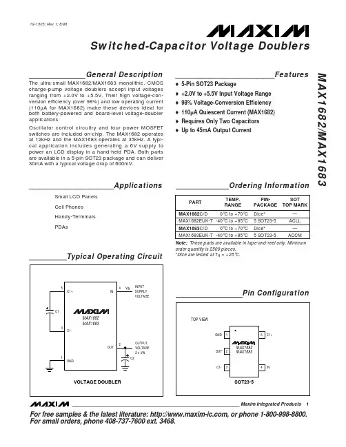
MAX1682-MAX1683中文资料
ELECTRICAL CHARACTERISTICS
(VIN = +5.0V, capacitor values from Table 2, TA = 0°C to +85°C, unless otherwise noted. Typical values are at TA = +25°C.) PARAMETER No-Load Supply Current Supply Voltage Range Minimum Operating Voltage Oscillator Frequency Output Resistance Voltage Conversion Efficiency TA = +25°C RLOAD = 10kΩ (Note 2) TA = +25°C IOUT = 5mA IOUT = 0mA, TA = +25°C MAX1682 MAX1683 TA = +25°C TA = 0°C to +85°C 98 99.9 8.4 24.5 CONDITIONS MAX1682 MAX1683 TA = +25°C TA = 0°C to +85°C 2.0 2.1 MIN TYP 110 230 1.7 1.8 1 12 35 20 15.6 45.5 50 65 MAX 145 310 5.5 5.5 UNITS µA V V kHz Ω %
OUTPUT RESISTANCE vs. SUPPLY VOLTAGE
80 OUTPUT RESISTANCE (Ω) 70 60 50 40 30 20 10 1.0 1.5 2.0 2.5 3.0 3.5 4.0 4.5 5.0 5.5 VIN (V) MAX1683, C1 = C2 = 10µF MAX1682, C1 = C2 = 10µF MAX1683, C1 = C2 = 3.3µF
MAX323_datasheet
________________General DescriptionThe MAX3222/MAX3232/MAX3237/MAX3241 trans-ceivers have a proprietary low-dropout transmitter out-put stage enabling true RS-232 performance from a 3.0V to 5.5V supply with a dual charge pump. The devices require only four small 0.1µF external charge-pump capacitors. The MAX3222, MAX3232, and MAX3241 are guaranteed to run at data rates of 120kbps while maintaining RS-232 output levels. The MAX3237 is guaranteed to run at data rates of 250kbps in the normal operating mode and 1Mbps in the MegaBaud™ operating mode, while maintaining RS-232output levels.The MAX3222/MAX3232 have 2 receivers and 2 drivers. The MAX3222 features a 1µA shutdown mode that reduces power consumption and extends battery life in portable systems. Its receivers remain active in shutdown mode, allowing external devices such as modems to be monitored using only 1µA supply cur-rent. The MAX3222 and MAX3232 are pin, package,and functionally compatible with the industry-standard MAX242 and MAX232, respectively.The MAX3241 is a complete serial port (3 drivers/5 receivers) designed for notebook and subnotebook computers. The MAX3237 (5 drivers/3 receivers) is ideal for fast modem applications. Both these devices feature a shutdown mode in which all receivers can remain active while using only 1µA supply current. Receivers R1(MAX3237/MAX3241) and R2 (MAX3241) have extra out-puts in addition to their standard outputs. These extra outputs are always active, allowing external devices such as a modem to be monitored without forward bias-ing the protection diodes in circuitry that may have V CC completely removed.The MAX3222, MAX3237, and MAX3241 are available in space-saving TSSOP and SSOP packages.________________________ApplicationsNotebook, Subnotebook, and Palmtop Computers High-Speed ModemsHand-Held Equipment Peripherals Printers3.0V to 5.5V , Low-Power , up to 1Mbps, T rue RS-232Transceivers Using Four 0.1µF External CapacitorsMegaBaud and UCSP are trademarks of Maxim Integrated Products, Inc.Typical Operating Circuits appear at end of data sheet.MAX3222/MAX3232/ MAX3237/MAX3241捷多邦,您值得信赖的PCB打样专家!3.0V to 5.5V , Low-Power , up to 1Mbps, T rue RS-232Transceivers Using Four 0.1µF External CapacitorsABSOLUTE MAXIMUM RATINGSELECTRICAL CHARACTERISTICS(V CC = +3.0V to +5.5V, C1–C4 = 0.1µF (Note 2), T A = T MIN to T MAX , unless otherwise noted. Typical values are at T A = +25°C.)Stresses beyond those listed under “Absolute Maximum Ratings” may cause permanent damage to the device. These are stress ratings only, and functional operation of the device at these or any other conditions beyond those indicated in the operational sections of the specifications is not implied. Exposure to absolute maximum rating conditions for extended periods may affect device reliability.Note 1:V+ and V- can have a maximum magnitude of 7V, but their absolute difference cannot exceed 13V.V CC ...........................................................................-0.3V to +6V V+ (Note 1)...............................................................-0.3V to +7V V- (Note 1)................................................................+0.3V to -7V V+ + V- (Note 1)...................................................................+13V Input VoltagesT_IN, SHDN , EN ...................................................-0.3V to +6V MBAUD...................................................-0.3V to (V CC + 0.3V)R_IN.................................................................................±25V Output VoltagesT_OUT...........................................................................±13.2V R_OUT....................................................-0.3V to (V CC + 0.3V)Short-Circuit DurationT_OUT....................................................................ContinuousContinuous Power Dissipation (T A = +70°C)16-Pin TSSOP (derate 6.7mW/°C above +70°C).............533mW 16-Pin Narrow SO (derate 8.70mW/°C above +70°C)....696mW 16-Pin Wide SO (derate 9.52mW/°C above +70°C)........762mW 16-Pin Plastic DIP (derate 10.53mW/°C above +70°C)...842mW 18-Pin SO (derate 9.52mW/°C above +70°C)..............762mW 18-Pin Plastic DIP (derate 11.11mW/°C above +70°C)..889mW 20-Pin SSOP (derate 7.00mW/°C above +70°C).........559mW 20-Pin TSSOP (derate 8.0mW/°C above +70°C).............640mW 28-Pin TSSOP (derate 8.7mW/°C above +70°C).............696mW 28-Pin SSOP (derate 9.52mW/°C above +70°C).........762mW 28-Pin SO (derate 12.50mW/°C above +70°C).....................1W Operating Temperature RangesMAX32_ _C_ _.....................................................0°C to +70°C MAX32_ _E_ _ .................................................-40°C to +85°C Storage Temperature Range.............................-65°C to +150°C Lead Temperature (soldering, 10s).................................+300°CMAX3222/MAX3232/MAX3237/MAX32413.0V to 5.5V , Low-Power , up to 1Mbps, T rue RS-232Transceivers Using Four 0.1µF External CapacitorsTIMING CHARACTERISTICS—MAX3222/MAX3232/MAX3241(V CC = +3.0V to +5.5V, C1–C4 = 0.1µF (Note 2), T A = T MIN to T MAX , unless otherwise noted. Typical values are at T A = +25°C.)ELECTRICAL CHARACTERISTICS (continued)(V CC = +3.0V to +5.5V, C1–C4 = 0.1µF (Note 2), T A = T MIN to T MAX , unless otherwise noted. Typical values are at T A = +25°C.)MAX3222/MAX3232/MAX3237/MAX32413.0V to 5.5V , Low-Power , up to 1Mbps, T rue RS-232Transceivers Using Four 0.1µF External Capacitors__________________________________________Typical Operating Characteristics(V CC = +3.3V, 235kbps data rate, 0.1µF capacitors, all transmitters loaded with 3k Ω, T A = +25°C, unless otherwise noted.)-6-5-4-3-2-101234560MAX3222/MAX3232TRANSMITTER OUTPUT VOLTAGEvs. LOAD CAPACITANCELOAD CAPACITANCE (pF)T R A N S M I T T E R O U T P U T V O L T A G E (V )20003000100040005000246810121416182022150MAX3222/MAX3232SLEW RATEvs. LOAD CAPACITANCELOAD CAPACITANCE (pF)S L E W R A T E (V /µs )20003000100040005000510152025303540MAX3222/MAX3232SUPPLY CURRENT vs. LOAD CAPACITANCEWHEN TRANSMITTING DATALOAD CAPACITANCE (pF)S U P P L Y C U R R E N T (m A )20003000100040005000TIMING CHARACTERISTICS—MAX3237(V CC = +3.0V to +5.5V, C1–C4 = 0.1µF (Note 2), T A = T MIN to T MAX , unless otherwise noted. Typical values are at T A = +25°C.)Note 2:MAX3222/MAX3232/MAX3241: C1–C4 = 0.1µF tested at 3.3V ±10%; C1 = 0.047µF, C2–C4 = 0.33µF tested at 5.0V ±10%.MAX3237: C1–C4 = 0.1µF tested at 3.3V ±5%; C1–C4 = 0.22µF tested at 3.3V ±10%; C1 = 0.047µF, C2–C4 = 0.33µF tested at 5.0V ±10%.Note 3:Transmitter input hysteresis is typically 250mV.MAX3222/MAX3232/MAX3237/MAX32413.0V to 5.5V , Low-Power , up to 1Mbps, T rue RS-232Transceivers Using Four 0.1µF External Capacitors-7.5-5.0-2.502.55.07.50MAX3241TRANSMITTER OUTPUT VOLTAGEvs. LOAD CAPACITANCELOAD CAPACITANCE (pF)T R A N S M I T T E R O U T P U T V O L T A G E (V )2000300010004000500046810121416182022240MAX3241SLEW RATEvs. LOAD CAPACITANCELOAD CAPACITANCE (pF)S L E W R A T E (V /µs )20003000100040005000510152025303545400MAX3241SUPPLY CURRENT vs. LOADCAPACITANCE WHEN TRANSMITTING DATALOAD CAPACITANCE (pF)S U P P L Y C U R R E N T (m A )20003000100040005000-7.5-5.0-2.502.55.07.50MAX3237TRANSMITTER OUTPUT VOLTAGE vs. LOAD CAPACITANCE (MBAUD = GND)LOAD CAPACITANCE (pF)T R A N S M I T T E R O U T P U T V O L T A G E (V )200030001000400050000102030504060700MAX3237SLEW RATE vs. LOAD CAPACITANCE(MBAUD = V CC )LOAD CAPACITANCE (pF)S L E W R A T E (V /µs )500100015002000-7.5-5.0-2.502.55.07.50MAX3237TRANSMITTER OUTPUT VOLTAGE vs. LOAD CAPACITANCE (MBAUD = V CC )LOAD CAPACITANCE (pF)T R A N S M I T T E R O U T P U T V O L T A G E (V )5001000150020001020304050600MAX3237SUPPLY CURRENT vs.LOAD CAPACITANCE (MBAUD = GND)LOAD CAPACITANCE (pF)S U P P L Y C U R R E N T(m A )200030001000400050000246810120MAX3237SLEW RATE vs. LOAD CAPACITANCE(MBAUD = GND)LOAD CAPACITANCE (pF)S L E W R A T E (V /µs )2000300010004000500010302040506070MAX3237SKEW vs. LOAD CAPACITANCE(t PLH - t PHL )LOAD CAPACITANCE (pF)1000150050020002500_____________________________Typical Operating Characteristics (continued)(V CC = +3.3V, 235kbps data rate, 0.1µF capacitors, all transmitters loaded with 3k Ω, T A = +25°C, unless otherwise noted.)MAX3222/MAX3232/MAX3237/MAX32413.0V to 5.5V , Low-Power , up to 1Mbps, T rue RS-232Transceivers Using Four 0.1µF External Capacitors______________________________________________________________Pin DescriptionMAX3222/MAX3232/MAX3237/MAX32413.0V to 5.5V , Low-Power , up to 1Mbps, T rue RS-232Transceivers Using Four 0.1µF External Capacitors_______________Detailed DescriptionDual Charge-Pump Voltage ConverterThe MAX3222/MAX3232/MAX3237/MAX3241’s internal power supply consists of a regulated dual charge pump that provides output voltages of +5.5V (doubling charge pump) and -5.5V (inverting charge pump), regardless of the input voltage (V CC ) over the 3.0V to 5.5V range. The charge pumps operate in a discontinuous mode; if the output voltages are less than 5.5V, the charge pumps are enabled, and if the output voltages exceed 5.5V, the charge pumps are disabled. Each charge pump requires a flying capacitor (C1, C2) and a reservoir capacitor (C3, C4) to generate the V+ and V- supplies.RS-232 TransmittersThe transmitters are inverting level translators that con-vert CMOS-logic levels to 5.0V EIA/TIA-232 levels.The MAX3222/MAX3232/MAX3241 transmitters guaran-tee a 120kbps data rate with worst-case loads of 3k Ωin parallel with 1000pF, providing compatibility with PC-to-PC communication software (such as LapLink™).Typically, these three devices can operate at data rates of 235kbps. Transmitters can be paralleled to drive multi-ple receivers or mice.The MAX3222/MAX3237/MAX3241’s output stage is turned off (high impedance) when the device is in shut-down mode. When the power is off, the MAX3222/MAX3232/MAX3237/MAX3241 permit the outputs to be driven up to ±12V.The transmitter inputs do not have pullup resistors.Connect unused inputs to GND or V CC .MAX3237 MegaBaud OperationIn normal operating mode (MBAUD = GND ), the MAX3237 transmitters guarantee a 250kbps data rate with worst-case loads of 3k Ωin parallel with 1000pF.This provides compatibility with PC-to-PC communica-tion software, such as Laplink.For higher speed serial communications, the MAX3237features MegaBaud operation. In MegaBaud operating mode (MBAUD = V CC ), the MAX3237 transmitters guar-antee a 1Mbps data rate with worst-case loads of 3k Ωin parallel with 250pF for 3.0V < V CC < 4.5V. For 5V ±10%operation, the MAX3237 transmitters guarantee a 1Mbps data rate into worst-case loads of 3k Ωin parallel with 1000pF.Figure 1. Slew-Rate Test CircuitsLapLink is a trademark of Traveling Software, Inc.MAX3222/MAX3232/MAX3237/MAX32413.0V to 5.5V , Low-Power , up to 1Mbps, T rue RS-232Transceivers Using Four 0.1µF External CapacitorsRS-232 ReceiversThe receivers convert RS-232 signals to CMOS-logic out-put levels. The MAX3222/MAX3237/MAX3241 receivers have inverting three-state outputs. In shutdown, the receivers can be active or inactive (Table 1).The complementary outputs on the MAX3237 (R1OUTB)and the MAX3241 (R1OUTB, R2OUTB) are always active,regardless of the state of EN or SHDN . This allows for Ring Indicator applications without forward biasing other devices connected to the receiver outputs. This is ideal for systems where V CC is set to 0V in shutdown to accommodate peripherals, such as UARTs (Figure 2).MAX3222/MAX3237/MAX3241Shutdown ModeSupply current falls to less than 1µA in shutdown mode (SHDN = low). When shut down, the device’s charge pumps are turned off, V+ is pulled down to V CC , V- is pulled to ground, and the transmitter outputs are dis-abled (high impedance). The time required to exit shut-down is typically 100µs, as shown in Figure 3. Connect SHDN to V CC if the shutdown mode is not used. SHDN has no effect on R_OUT or R_OUTB.MAX3222/MAX3237/MAX3241Enable ControlThe inverting receiver outputs (R_OUT) are put into a high-impedance state when EN is high. The complemen-tary outputs R1OUTB and R2OUTB are always active,regardless of the state of EN and SHDN (Table 1). EN has no effect on T_OUT.__________Applications InformationCapacitor SelectionThe capacitor type used for C1–C4 is not critical for proper operation; polarized or nonpolarized capacitors can be used. The charge pump requires 0.1µF capaci-tors for 3.3V operation. For other supply voltages, refer to Table 2 for required capacitor values. Do not use values lower than those listed in Table 2. Increasing the capaci-tor values (e.g., by a factor of 2) reduces ripple on the transmitter outputs and slightly reduces power consump-tion. C2, C3, and C4 can be increased without changing C1’s value. However, do not increase C1 without also increasing the values of C2, C3, and C4, to maintain the proper ratios (C1 to the other capacitors).When using the minimum required capacitor values,make sure the capacitor value does not degrade exces-sively with temperature. If in doubt, use capacitors with a higher nominal value. The capacitor’s equivalent series resistance (ESR), which usually rises at low tempera-tures, influences the amount of ripple on V+ and V-.Figure 2. Detection of RS-232 Activity when the UART and Interface are Shut Down; Comparison of MAX3237/MAX3241(b) with Previous Transceivers (a).MAX3222/MAX3232/MAX3237/MAX32413.0V to 5.5V , Low-Power , up to 1Mbps, T rue RS-232Transceivers Using Four 0.1µF External CapacitorsPower-Supply DecouplingIn most circumstances, a 0.1µF bypass capacitor is adequate. In applications that are sensitive to power-supply noise, decouple V CC to ground with a capacitor of the same value as charge-pump capacitor C1. Connect bypass capacitors as close to the IC as possible.Operation Down to 2.7VTransmitter outputs will meet EIA/TIA-562 levels of ±3.7V with supply voltages as low as 2.7V.Transmitter Outputs whenExiting ShutdownFigure 3 shows two transmitter outputs when exiting shutdown mode. As they become active, the two trans-mitter outputs are shown going to opposite RS-232 lev-els (one transmitter input is high, the other is low).Each transmitter is loaded with 3k Ωin parallel with 2500pF. The transmitter outputs display no ringing or undesirable transients as they come out of shutdown.Note that the transmitters are enabled only when the magnitude of V- exceeds approximately 3V.Mouse DriveabilityThe MAX3241 has been specifically designed to power serial mice while operating from low-voltage power sup-plies. It has been tested with leading mouse brands from manufacturers such as Microsoft and Logitech. The MAX3241 successfully drove all serial mice tested and met their respective current and voltage requirements.Figure 4a shows the transmitter output voltages under increasing load current at 3.0V. Figure 4b shows a typical mouse connection using the MAX3241.CC = 3.3V C1–C4 = 0.1µF50µs/divFigure 3. Transmitter Outputs when Exiting Shutdown or Powering UpMAX3222/MAX3232/MAX3237/MAX32413.0V to 5.5V , Low-Power , up to 1Mbps, T rue RS-232Transceivers Using Four 0.1µF External CapacitorsFigure 4b. Mouse Driver Test CircuitFigure 4a. MAX3241 Transmitter Output Voltage vs. Load Current per TransmitterMAX3222/MAX3232/MAX3237/MAX32413.0V to 5.5V, Low-Power, up to 1Mbps, T rue RS-232Transceivers Using Four 0.1µF External CapacitorsHigh Data RatesThe MAX3222/MAX3232/MAX3241 maintain the RS-232±5.0V minimum transmitter output voltage even at highdata rates. Figure 5 shows a transmitter loopback testcircuit. Figure 6 shows a loopback test result at120kbps, and Figure 7 shows the same test at 235kbps.For Figure 6, all transmitters were driven simultaneouslyat 120kbps into RS-232 loads in parallel with 1000pF.For Figure 7, a single transmitter was driven at 235kbps,and all transmitters were loaded with an RS-232 receiverin parallel with 1000pF.The MAX3237 maintains the RS-232 ±5.0V minimumtransmitter output voltage at data rates up to 1Mbps.Figure 8 shows a loopback test result at 1Mbps withMBAUD = V CC. For Figure 8, all transmitters wereloaded with an RS-232 receiver in parallel with 250pF.CC = 3.3V5µs/divFigure 5. Loopback Test CircuitFigure 6. MAX3241 Loopback Test Result at 120kbpsCC = 3.3V2µs/divFigure 7. MAX3241 Loopback Test Result at 235kbps0V +5V 0V -5V +5V 0VT_INT_OUT = R_IN5kR_OUT150pF200ns/divCC = 3.3VFigure 8. MAX3237 Loopback Test Result at 1000kbps(MBAUD = V CC)MAX3222/MAX3232/MAX3237/MAX32413.0V to 5.5V , Low-Power , up to 1Mbps, T rue RS-232Transceivers Using Four 0.1µF External Capacitors__________________________________________________Typical Operating CircuitsInterconnection with 3V and 5V LogicThe MAX3222/MAX3232/MAX3237/MAX3241 can directly interface with various 5V logic families, includ-ing ACT and HCT CMOS. See Table 3 for more informa-tion on possible combinations of interconnections.Table 3. Logic-Family Compatibility with Various Supply VoltagesMAX3222/MAX3232/MAX3237/MAX3241MAX3222/MAX3232/MAX3237/MAX3241 3.0V to 5.5V, Low-Power, up to 1Mbps, T rue RS-232Transceivers Using Four 0.1µF External Capacitors_____________________________________Typical Operating Circuits (continued)MAX3222/MAX3232/MAX3237/MAX32413.0V to 5.5V, Low-Power, up to 1Mbps, T rue RS-232 Transceivers Using Four 0.1µF External Capacitors_____________________________________________Pin Configurations (continued)3.0V to 5.5V , Low-Power , up to 1Mbps, T rue RS-232Transceivers Using Four 0.1µF External Capacitors______3V-Powered EIA/TIA-232 and EIA/TIA-562 Transceivers from MaximOrdering Information (continued)*Dice are tested at T A = +25°C, DC parameters only.+Denotes lead-free package.MAX3222/MAX3232/MAX3237/MAX32413.0V to 5.5V , Low-Power , up to 1Mbps, T rue RS-232Transceivers Using Four 0.1µF External Capacitors___________________Chip Topography___________________Chip InformationT1INT2IN 0.127"(3.225mm)0.087"(2.209mm)R2OUTR2IN T2OUTV CCV+C1+SHDNENC1- C2+C2-V-MAX3222TRANSISTOR COUNT: 339SUBSTRATE CONNECTED TO GNDMAX3222/MAX3232/MAX3237/MAX32413.0V to 5.5V , Low-Power , up to 1Mbps, T rue RS-232Transceivers Using Four 0.1µF External CapacitorsPackage Information(The package drawing(s) in this data sheet may not reflect the most current specifications. For the latest package outline information,go to /packages .)Revision HistoryPages changed at Rev 7: 1, 15, 16, 17MAX3222/MAX3232/MAX3237/MAX3241Maxim Integrated 160 Rio Robles, San Jose, CA 95134 USA 1-408-601-1000Maxim cannot assume responsibility for use of any circuitry other than circuitry entirely embodied in a Maxim product. No circuit patent licenses are implied. Maxim reserves the right to change the circuitry and specifications without notice at any time. The parametric values (min and max limits) shown in the Electrical Characteristics table are guaranteed. Other parametric values quoted in this data sheet are provided for guidance.©2007 Maxim IntegratedThe Maxim logo and Maxim Integrated are trademarks of Maxim Integrated Products, Inc.。
MAX4130EUK+T,MAX4130EUK+T,MAX4132ESA+,MAX4132EUA+,MAX4131ESA,MAX4131EBT+T, 规格书,Datasheet 资料
MAX4130–MAX4134________________________________________________________________Maxim Integrated Products1For pricing, delivery, and ordering information,please contact Maxim/Dallas Direct!at 1-888-629-4642, or visit Maxim’s website at .General DescriptionThe MAX4130–MAX4134 family of operational amplifiers combines 10MHz gain-bandwidth product and excellent DC accuracy with Rail-to-Rail ®operation at the inputs and outputs. These devices require only 900µA per amplifier, and operate from either a single supply (+2.7V to +6.5V) or dual supplies (±1.35V to ±3.25V) with a common-mode voltage range that extends 250mV beyond V EE and V CC . They are capable of driving 250Ωloads and are unity-gain stable. In addition, the MAX4131/ MAX4133 feature a shutdown mode in which the outputs are placed in a high-impedance state and the supply current is reduced to only 25µA per amplifier.With their rail-to-rail input common-mode range and output swing, the MAX4130–MAX4134 are ideal for low-voltage, single-supply operation. Although the minimum operating voltage is specified at 2.7V, the devices typically operate down to 1.8V. In addition, low offset voltage and high speed make them the ideal signal-conditioning stages for precision, low-voltage data-acquisition systems. The MAX4130 is offered in the space-saving 5-pin SOT23 package. The MAX4131 is offered in the ultra-small 6-bump, 1mm x 1.5mm chip-scale package (UCSP™).________________________ApplicationsBattery-Powered Instruments Portable Equipment Data-Acquisition Systems Signal ConditioningLow-Power, Low-Voltage ApplicationsFeatureso 6-Bump UCSP (MAX4131)o +2.7V to +6.5V Single-Supply Operationo Rail-to-Rail Input Common-Mode Voltage Rangeo Rail-to-Rail Output Voltage Swing o 10MHz Gain-Bandwidth Product o 900µA Quiescent Current per Amplifier o 25µA Shutdown Function (MAX4131/MAX4133)o 200µV Offset Voltageo No Phase Reversal for Overdriven Inputs o Drive 250ΩLoadso Stable with 160pF Capacitive Loads o Unity-Gain StableSingle/Dual/Quad, Wide-Bandwidth, Low-Power,Single-Supply, Rail-to-Rail I/O Op Amps19-1089; Rev 3; 3/03*Dice are specified at T A = +25°C. DC parameters only.Ordering Information continued at end of data sheet.Pin Configurations appear at end of data sheet.Rail-to-Rail is a registered trademark of Nippon Motorola, Ltd.UCSP is a trademark of Maxim Integrated Products, Inc.M A X 4130–M A X 4134Single/Dual/Quad, Wide-Bandwidth, Low-Power,Single-Supply Rail-to-Rail I/O Op Amps 2_______________________________________________________________________________________ABSOLUTE MAXIMUM RATINGSDC ELECTRICAL CHARACTERISTICS(V CC = +2.7V to +6.5V, V EE = 0V, V CM = 0V, V OUT = V CC /2, R L tied to V CC /2, SHDN ≥2V (or open), T A = +25°C , unless otherwise noted.)Stresses beyond those listed under “Absolute Maximum Ratings” may cause permanent damage to the device. These are stress ratings only, and functional operation of the device at these or any other conditions beyond those indicated in the operational sections of the specifications is not implied. Exposure to absolute maximum rating conditions for extended periods may affect device reliability.Supply Voltage (V CC - V EE )...................................................7.5V IN+, IN-, SHDN Voltage...................(V CC + 0.3V) to (V EE - 0.3V)Output Short-Circuit Duration (Note 1).......................Continuous(short to either supply)Continuous Power Dissipation (T A = +70°C)5-Pin SOT23 (derate 7.1mW/°C above +70°C)............571mW 6-Bump UCSP (derate 2.9mW/°C above +70°C).........308mW 8-Pin SO (derate 5.88mW/°C above +70°C)................471mW8-Pin µMAX (derate 4.10mW/°C above +70°C)...........330mW 14-Pin SO (derate 8.00mW/°C above +70°C)..............640mW Operating Temperature RangeMAX413_E__...................................................-40°C to +85°C Maximum Junction Temperature.....................................+150°C Storage Temperature Range.............................-65°C to +160°C Lead Temperature (soldering, 10s).................................+300°C Bump Reflow Temperature .........................................+235°CNote 1:Provided that the maximum package power-dissipation rating is not exceeded.MAX4130–MAX4134Single/Dual/Quad, Wide-Bandwidth, Low-Power,Single-Supply Rail-to-Rail I/O Op AmpsDC ELECTRICAL CHARACTERISTICS (continued)(V CC = +2.7V to +6.5V, V EE = 0V, V CM = 0V, V OUT = V CC /2, R L tied to V CC /2, SHDN ≥2V (or open), T A = +25°C , unless otherwise noted.)DC ELECTRICAL CHARACTERISTICS(V CC = +2.7V to +6.5V, V EE = 0V, V CM = 0V, V OUT = V CC /2, R L tied to V CC /2, SHDN ≥2V (or open), T A = -40°C to +85°C , unlessM A X 4130–M A X 4134Single/Dual/Quad, Wide-Bandwidth, Low-Power,Single-Supply Rail-to-Rail I/O Op Amps 4_______________________________________________________________________________________DC ELECTRICAL CHARACTERISTICS(V CC = +2.7V to +6.5V, V EE = 0V, V CM = 0V, V OUT = V CC /2, R L tied to V CC /2, SHDN ≥2V (or open), T A = -40°C to +85°C , unlessMAX4130–MAX4134Single/Dual/Quad, Wide-Bandwidth, Low-Power,Single-Supply Rail-to-Rail I/O Op Amps_______________________________________________________________________________________5DC ELECTRICAL CHARACTERISTICS (continued)(V CC = +2.7V to +6.5V, V EE = 0V, V CM = 0V, V OUT = V CC /2, R L tied to V CC /2, SHDN ≥2V (or open), T A = -40°C to +85°C , unless otherwise noted.) (Note 2)AC ELECTRICAL CHARACTERISTICSM A X 4130–M A X 4134Single/Dual/Quad, Wide-Bandwidth, Low-Power,Single-Supply, Rail-to-Rail I/O Op Amps 6_______________________________________________________________________________________60-401001k 10k 1M 10M100k 100M GAIN AND PHASE vs. FREQUENCY-20FREQUENCY (Hz)G A I N (d B )02040P H A S E (D E G R E E S )180144720-72-144-180-108-363610860-401001k 10k 1M 10M100k 100MGAIN AND PHASEvs. FREQUENCY (WITH C)-20FREQUENCY (Hz)G A I N (d B )2040P H A S E (D E G R E E S )180144720-72-144-180-108-36361080-100101001k100k1M10M10k 100MPOWER-SUPPLY REJECTIONvs. FREQUENCY-80FREQUENCY (Hz)P S R (d B )-60-40-2001051520253530454050-40-25-105203550658095SHUTDOWN SUPPLY CURRENTvs. TEMPERATURETEMPERATURE (°C)S U P P L Y C U R R E N T (µA )1000.100.011001k100k1M10M10k100MOUTPUT IMPEDANCE vs. FREQUENCYFREQUENCY (Hz)O U T P U T I M P E D A N C E (Ω)1101150800850900950105010001100-40-25-105203550658095SUPPLY CURRENT PER AMPLIFIERvs. TEMPERATURETEMPERATURE (°C)S U P P L Y C U R R E N T (µA )-10-505101520-40-25-105203550658095OUTPUT LEAKAGE CURRENTvs. TEMPERATURETEMPERATURE (°C)L E A K A G E C U R R E N T (µA )Typical Operating Characteristics(V CC = +5V, V EE = 0V, VCM = V CC / 2, T A = +25°C, unless otherwise noted.)-600123456INPUT BIAS CURRENT vs. COMMON-MODE VOLTAGECOMMON-MODE VOLTAGE (V)I N P U T B I A S C U R R E N T (n A )-50-40-30-20-10010203040-60-40-40-25-105203550658095INPUT BIAS CURRENTvs. TEMPERATURETEMPERATURE (°C)I N P U T B I A S C U R R E N T (n A )-200204060MAX4130–MAX4134Single/Dual/Quad, Wide-Bandwidth, Low-Power,Single-Supply, Rail-to-Rail I/O Op Amps_______________________________________________________________________________________712070750600110115OUTPUT VOLTAGE: EITHER SUPPLY (mV)G A I N (d B )30095859080100200500105100400LARGE-SIGNAL GAIN vs. OUTPUT VOLTAGE130-40-25-105203550658095LARGE-SIGNAL GAIN vs. TEMPERATURE90120TEMPERATURE (°C)G A I N (d B )11010085951251151051.21.31.51.41.61.71.81.9-40-25-105203550658095MINIMUM OPERATING VOLTAGEvs. TEMPERATUREM A X 4130/34-21TEMPERATURE (°C)M I N I M U M O P E R A T I N G V O L T A G E (V )Typical Operating Characteristics (continued)(V CC = +5V, V EE = 0V, V CM = V CC / 2, T A = +25°C, unless otherwise noted.)12080859095100105110115-40-25-105203550658095COMMON-MODE REJECTIONvs. TEMPERATURETEMPERATURE (°C)C O M M O N -M ODE R E J E C T I O N (d B )130700600120OUTPUT VOLTAGE: EITHER SUPPLY (mV)G A I N (dB )3001009080100200500110400LARGE-SIGNAL GAIN vs. OUTPUT VOLTAGE12060600110OUTPUT VOLTAGE: EITHER SUPPLY (mV)G A I N (d B )300908070100200500100400LARGE-SIGNAL GAIN vs. OUTPUT VOLTAGE12080-40-25-105203550658095LARGE-SIGNAL GAIN vs. TEMPERATURE90TEMPERATURE (°C)G A I N (d B )105859511511010012070750600110115OUTPUT VOLTAGE: EITHER SUPPLY (mV)G A I N (d B )30095859080100200500105100400LARGE-SIGNAL GAIN vs. OUTPUT VOLTAGE-3.00-2.25-0.75-1.5001.500.752.253.00-40-25-105203550658095INPUT OFFSET VOLTAGE vs. TEMPERATURETEMPERATURE (°C)V O L T A G E (m V )M A X 4130–M A X 4134Single/Dual/Quad, Wide-Bandwidth, Low-Power,Single-Supply, Rail-to-Rail I/O Op Amps 8_______________________________________________________________________________________1408010k 1k 100k 10M 1M CHANNEL SEPARATION vs. FREQUENCYFREQUENCY (Hz)C H A N N E L S E P A R A T I O N (d B )1009013011012010100k10kFREQUENCY (Hz)1001k 0.03000.0050.0100.0150.0200.025 TOTAL HARMONIC DISTORTION AND NOISE vs. FREQUENCYT H D A N D N O I S E (%)0.10.0014.04.44.25.04.84.6TOTAL HARMONIC DISTORTION AND NOISE vs. PEAK-TO-PEAK SIGNAL AMPLITUDEPEAK-TO-PEAK SIGNAL AMPLITUDE (V)T H D + N O I S E (%)0.01INTIME (200ns/div)V O L T A G E (50m V /d i v )OUTMAX4131SMALL-SIGNAL TRANSIENT RESPONSE (NONINVERTING)IN TIME (200ns/div)V O L T A G E (50m V /d i v )OUT MAX4131SMALL-SIGNAL TRANSIENT RESPONSE (INVERTING)A V = -1IN TIME (2µs/div)V O L T A G E (2V/d i v )OUT MAX4131LARGE-SIGNAL TRANSIENT RESPONSE (NONINVERTING)A V = +1INTIME (2µs/div)V O L T A G E (2V /d i v )OUTMAX4131LARGE-SIGNAL TRANSIENT RESPONSE (INVERTING)Typical Operating Characteristics (continued)(V CC = +5V, V EE = 0V, V CM = V CC / 2, T A = +25°C, unless otherwise noted.)1600-40-25-105203550658095MINIMUM OUTPUT VOLTAGEvs. TEMPERATURE20140120TEMPERATURE (°C)V O U T - V E E (m V )100806040050100150200250300-40-25-105203550658095MAXIMUM OUTPUT VOLTAGEvs. TEMPERATURETEMPERATURE (°C)V C C - V O U T (m V )MAX4130–MAX4134Single/Dual/Quad, Wide-Bandwidth, Low-Power,Single-Supply, Rail-to-Rail I/O Op Amps_______________________________________________________________________________________9Figure 1a. Reducing Offset Error Due to Bias Current (Noninverting)Figure 1b. Reducing Offset Error Due to Bias Current (Inverting)M A X 4130–M A X 4134Single/Dual/Quad, Wide-Bandwidth, Low-Power,Single-Supply, Rail-to-Rail I/O Op Amps 10______________________________________________________________________________________Applications InformationRail-to-Rail Input StageDevices in the MAX4130–MAX4134 family of high-speed amplifiers have rail-to-rail input and output stages designed for low-voltage, single-supply opera-tion. The input stage consists of separate NPN and PNP differential stages that combine to provide an input common-mode range that extends 0.2V beyond the supply rails. The PNP stage is active for input volt-ages close to the negative rail, and the NPN stage is active for input voltages near the positive rail. The input offset voltage is typically below 200µV. The switchover transition region, which occurs near V CC / 2, has been extended to minimize the slight degradation in com-mon-mode rejection ratio caused by the mismatch of the input pairs. Their low offset voltage, high band-width, and rail-to-rail common-mode range make these op amps excellent choices for precision, low-voltage data-acquisition systems.Since the input stage switches between the NPN and PNP pairs, the input bias current changes polarity as the input voltage passes through the transition region.Reduce the offset error caused by input bias currents flowing through external source impedances by match-ing the effective impedance seen by each input (Figures 1a, 1b). High source impedances, together with input capacitance, can create a parasitic pole that produces an underdamped signal response. Reducing the input impedance or placing a small (2pF to 10pF)capacitor across the feedback resistor improves response.The MAX4130–MAX4134s ’ inputs are protected from large differential input voltages by 1k Ωseries resistors and back-to-back triple diodes across the inputs (Figure 2). For differential input voltages less than 1.8V,input resistance is typically 500k Ω. For differential input voltages greater than 1.8V, input resistance is approxi-mately 2k Ω. The input bias current is given by the fol-lowing equation:Figure 2. Input Protection CircuitMAX4130–MAX4134Single/Dual/Quad, Wide-Bandwidth, Low-Power,Single-Supply, Rail-to-Rail I/O Op Amps______________________________________________________________________________________11Rail-to-Rail Output StageThe minimum output voltage is within millivolts of ground for single-supply operation where the load is referenced to ground (V EE ). Figure 3 shows the input voltage range and output voltage swing of a MAX4131connected as a voltage follower. With a +3V supply and the load tied to ground, the output swings from 0.00V to 2.90V. The maximum output voltage swing depends on the load, but will be within 150mV of a +3V supply, even with the maximum load (500Ωto ground).Driving a capacitive load can cause instability in most high-speed op amps, especially those with low quies-cent current. The MAX4130–MAX4134 have a high tol-erance for capacitive loads. They are stable with capacitive loads up to 160pF. Figure 4 gives the stable operating region for capacitive loads. Figures 5 and 6show the response with capacitive loads and the results of adding an isolation resistor in series with the output (Figure 7). The resistor improves the circuit ’s phase margin by isolating the load capacitor from the op amp ’s output.INTIME (1µs/div)V O L T A G E (1V /d i v )OUTV CC = 3V, R L = 10k Ω to V EEFigure 3. Rail-to-Rail Input/Output Voltage RangeFigure 4. Capacitive-Load StabilityINTIME (200ns/div)V O L T A G E (50m V /d i v )OUTV CC = 5V R L = 10k Ω C L = 130pFFigure 5. MAX4131 Small-Signal Transient Response with Capacitive Load Figure 6. MAX4131 Transient Response to Capacitive Load with Isolation ResistorINTIME (500ns/div)V O L T A G E (50m V /d i v )OUTV CC = 5V C L = 1000pF R S = 39ΩM A X 4130–M A X 4134Single/Dual/Quad, Wide-Bandwidth, Low-Power,Single-Supply, Rail-to-Rail I/O Op Amps 12______________________________________________________________________________________Power-Up and Shutdown ModeThe MAX4130–MAX4134 amplifiers typically settle with-in 1µs after power-up. Figures 9 and 10 show the out-put voltage and supply current on power-up, using the test circuit of Figure 8.The MAX4131 and MAX4133 have a shutdown option.When the shutdown pin (SHDN ) is pulled low, the sup-ply current drops below 25µA per amplifier and theamplifiers are disabled with the outputs in a high-impedance state. Pulling SHDN high or leaving it float-ing enables the amplifier. In the dual-amplifier MAX4133, the shutdown functions operate indepen-dently. Figures 11 and 12 show the output voltage and supply current responses of the MAX4131 to a shut-down pulse, using the test circuit of Figure 8.Figure 7. Capacitive-Load Driving CircuitFigure 8. Power-Up/Shutdown Test CircuitV CC TIME (5µs/div)V O L T A G E (1V /d i v )OUTFigure 9. Power-Up Output Voltage V CC (1V/div)TIME (5µs/div)I EE(500µA/div)Figure 10. Power-Up Supply CurrentMAX4130–MAX4134Single/Dual/Quad, Wide-Bandwidth, Low-Power,Single-Supply, Rail-to-Rail I/O Op Amps______________________________________________________________________________________13Power Supplies and LayoutThe MAX4130–MAX4134 operate from a single +2.7V to +6.5V power supply, or from dual supplies of ±1.35V to ±3.25V. For single-supply operation, bypass the power supply with a 0.1µF ceramic capacitor in parallel with at least 1µF. For dual supplies, bypass each sup-ply to ground.Good layout improves performance by decreasing the amount of stray capacitance at the op amp ’s inputs and outputs. Decrease stray capacitance by placing external components close to the op amp ’s pins, mini-mizing trace lengths and resistor leads.UCSP Applications InformationFor the latest application details on UCSP construction,dimensions, tape carrier information, PC board tech-niques, bump-pad layout, and the recommended reflow temperature profile, as well as the latest informa-tion on reliability testing results, go to Maxim ’s website at /ucsp and search for the Application Note: UCSP –A Wafer-Level Chip-Scale Package .TIME (1µs/div)OUTFigure 11. Shutdown Output Voltage TIME (1µs/div)Figure 12. Shutdown Enable/Disable Supply CurrentM A X 4130–M A X 4134Single/Dual/Quad, Wide-Bandwidth, Low-Power,Single-Supply, Rail-to-Rail I/O Op Amps 14________________________________________________________________________________________________________________________________________________Pin ConfigurationsMAX4130–MAX4134Single/Dual/Quad, Wide-Bandwidth, Low-Power,Single-Supply, Rail-to-Rail I/O Op Amps______________________________________________________________________________________15Chip InformationOrdering Information (continued)MAX4130 TRANSISTOR COUNT: 170MAX4131 TRANSISTOR COUNT: 170MAX4132 TRANSISTOR COUNT: 340MAX4134 TRANSISTOR COUNT: 680*Dice are specified at T A = +25°C, DC parameters only.Package Information(The package drawing(s) in this data sheet may not reflect the most current specifications. For the latest package outline information,go to /packages .)M A X 4130–M A X 4134Single/Dual/Quad, Wide-Bandwidth, Low-Power,Single-Supply, Rail-to-Rail I/O Op Amps 16______________________________________________________________________________________Package Information (continued)(The package drawing(s) in this data sheet may not reflect the most current specifications. For the latest package outline information,go to /packages .)MAX4130–MAX4134Single/Dual/Quad, Wide-Bandwidth, Low-Power,Single-Supply, Rail-to-Rail I/O Op Amps______________________________________________________________________________________17Package Information (continued)(The package drawing(s) in this data sheet may not reflect the most current specifications. For the latest package outline information,go to /packages .)Maxim cannot assume responsibility for use of any circuitry other than circuitry entirely embodied in a Maxim product. No circuit patent licenses are M A X 4130–M A X 4134Single/Dual/Quad, Wide-Bandwidth, Low-Power,Single-Supply, Rail-to-Rail I/O Op Amps implied. Maxim reserves the right to change the circuitry and specifications without notice at any time.18__________________Maxim Integrated Products, 120 San Gabriel Drive, Sunnyvale, CA 94086 (408) 737-7600©2003 Maxim Integrated ProductsPrinted USAis a registered trademark of Maxim Integrated Products.Package Information (continued)(The package drawing(s) in this data sheet may not reflect the most current specifications. For the latest package outline information,go to /packages .)。
PT6311N;PT6312N;PT6312R;PT6313A;PT6312B;中文规格书,Datasheet资料
For assistance or to order , call (800) 531-5782Power Trends, Inc. 27715 Diehl Road, Warrenville, IL 60555 (800) 531-5782 Fax: (630) 393-6902 /powertrendsPACKAGING INFORMATIONOrderable DeviceStatus (1)Package Type Package Drawing Pins Package Qty Eco Plan (2)Lead/Ball FinishMSL Peak Temp (3)PT6311N NRND SIP MOD ULE EBD 1212TBD Call TI Level-1-215C-UNLIM PT6312N NRND SIP MOD ULE EBD 1212TBD Call TI Level-1-215C-UNLIM PT6312R NRND SIP MOD ULE EBE 1212TBD Call TI Level-1-215C-UNLIM PT6313ANRNDSIP MOD ULEEBA1212Pb-Free (RoHS)Call TIN /A for Pkg Type(1)The marketing status values are defined as follows:ACTIVE:Product device recommended for new designs.LIFEBUY:TI has announced that the device will be discontinued,and a lifetime-buy period is in effect.NRND:Not recommended for new designs.Device is in production to support existing customers,but TI does not recommend using this part in a new design.PREVIEW:Device has been announced but is not in production.Samples may or may not be available.OBSOLETE:TI has discontinued the production of the device.(2)Eco Plan -The planned eco-friendly classification:Pb-Free (RoHS),Pb-Free (RoHS Exempt),or Green (RoHS &no Sb/Br)-please check /productcontent for the latest availability information and additional product content details.TBD:The Pb-Free/Green conversion plan has not been defined.Pb-Free (RoHS):TI's terms "Lead-Free"or "Pb-Free"mean semiconductor products that are compatible with the current RoHS requirements for all 6substances,including the requirement that lead not exceed 0.1%by weight in homogeneous materials.Where designed to be soldered at high temperatures,TI Pb-Free products are suitable for use in specified lead-free processes.Pb-Free (RoHS Exempt):This component has a RoHS exemption for either 1)lead-based flip-chip solder bumps used between the die and package,or 2)lead-based die adhesive used between the die and leadframe.The component is otherwise considered Pb-Free (RoHS compatible)as defined above.Green (RoHS &no Sb/Br):TI defines "Green"to mean Pb-Free (RoHS compatible),and free of Bromine (Br)and Antimony (Sb)based flame retardants (Br or Sb do not exceed 0.1%by weight in homogeneous material)(3)MSL,Peak Temp.--The Moisture Sensitivity Level rating according to the JEDEC industry standard classifications,and peak solder temperature.Important Information and Disclaimer:The information provided on this page represents TI's knowledge and belief as of the date that it is provided.TI bases its knowledge and belief on information provided by thirdparties,and makes no representation or warranty as to the accuracy of such information.Efforts are underway to better integrate information from third parties.TI has taken and continues to take reasonable steps to provide representative and accurate information but may not have conducted destructive testing or chemical analysis on incoming materials and chemicals.TI and TI suppliers consider certain information to be proprietary,and thus CAS numbers and other limited information may not be available for release.In no event shall TI's liability arising out of such information exceed the total purchase price of the TI part(s)at issue in this document sold by TI to Customer on an annual basis.PACKAGE OPTION ADDENDUM3-Jul-2009Addendum-Page 1IMPORTANT NOTICETexas Instruments Incorporated and its subsidiaries (TI)reserve the right to make corrections,modifications,enhancements,improvements,and other changes to its products and services at any time and to discontinue any product or service without notice.Customers should obtain the latest relevant information before placing orders and should verify that such information is current and complete.All products are sold subject to TI’s terms and conditions of sale supplied at the time of order acknowledgment.TI warrants performance of its hardware products to the specifications applicable at the time of sale in accordance with TI’s standard warranty.Testing and other quality control techniques are used to the extent TI deems necessary to support this warranty.Except where mandated by government requirements,testing of all parameters of each product is not necessarily performed.TI assumes no liability for applications assistance or customer product design.Customers are responsible for their products andapplications using TI components.To minimize the risks associated with customer products and applications,customers should provide adequate design and operating safeguards.TI does not warrant or represent that any license,either express or implied,is granted under any TI patent right,copyright,mask work right,or other TI intellectual property right relating to any combination,machine,or process in which TI products or services are rmation published by TI regarding third-party products or services does not constitute a license from TI to use such products or services or a warranty or endorsement e of such information may require a license from a third party under the patents or other intellectual property of the third party,or a license from TI under the patents or other intellectual property of TI.Reproduction of TI information in TI data books or data sheets is permissible only if reproduction is without alteration and is accompanied by all associated warranties,conditions,limitations,and notices.Reproduction of this information with alteration is an unfair and deceptive business practice.TI is not responsible or liable for such altered rmation of third parties may be subject to additional restrictions.Resale of TI products or services with statements different from or beyond the parameters stated by TI for that product or service voids all express and any implied warranties for the associated TI product or service and is an unfair and deceptive business practice.TI is not responsible or liable for any such statements.TI products are not authorized for use in safety-critical applications (such as life support)where a failure of the TI product would reasonably be expected to cause severe personal injury or death,unless officers of the parties have executed an agreement specifically governing such use.Buyers represent that they have all necessary expertise in the safety and regulatory ramifications of their applications,andacknowledge and agree that they are solely responsible for all legal,regulatory and safety-related requirements concerning their products and any use of TI products in such safety-critical applications,notwithstanding any applications-related information or support that may be provided by TI.Further,Buyers must fully indemnify TI and its representatives against any damages arising out of the use of TI products in such safety-critical applications.TI products are neither designed nor intended for use in military/aerospace applications or environments unless the TI products are specifically designated by TI as military-grade or "enhanced plastic."Only products designated by TI as military-grade meet militaryspecifications.Buyers acknowledge and agree that any such use of TI products which TI has not designated as military-grade is solely at the Buyer's risk,and that they are solely responsible for compliance with all legal and regulatory requirements in connection with such use.TI products are neither designed nor intended for use in automotive applications or environments unless the specific TI products are designated by TI as compliant with ISO/TS 16949requirements.Buyers acknowledge and agree that,if they use any non-designated products in automotive applications,TI will not be responsible for any failure to meet such requirements.Following are URLs where you can obtain information on other Texas Instruments products and application solutions:Products Applications AmplifiersAudioData Converters Automotive DLP®Products Broadband DSPDigital Control Clocks and Timers Medical Interface MilitaryLogicOptical Networking Power Mgmt Security Microcontrollers TelephonyRFIDVideo &Imaging RF/IF and ZigBee®SolutionsWirelessMailing Address:Texas Instruments,Post Office Box 655303,Dallas,Texas 75265Copyright ©2009,Texas Instruments Incorporatedht t p ://o分销商库存信息:TIPT6311N PT6312N PT6312R PT6313A PT6312B PT6313C PT6313N。
MAX8632笔记本电脑内存供电控制芯片
MAX8632笔记本电脑内存供电控制芯片P O K 2P O K 1I L I MR E FO V P /U V PT O NS T B YMAX8632MAX8632是笔记本电脑中常用的内存供电或芯片组供电控制芯片,内部集成了一路用于产生VDDQ的同步降压PWM控制器,一路用于产生VTT电源输出和吸入电流的LDO线性稳压器,另一路用于产生VTTR的10mA基准输出缓冲器。
引脚号引脚名称引脚功能1TON 导通时间选择输入端。
该四电平逻辑输入用来设置额定DH 导通时间。
TON分别连接至GND、REF、AVDD及悬空时可选择不同额定开关频率2OVP/UVP 过压/欠压保护控制输入端。
该四电平逻辑输入用来使能/禁止过压/欠压保护。
过压门限值为额定输出电压的116%。
欠压门限值为额定输出电压的70%。
使能OVP的同时启动放电模式3REF +2.0V基准电压输出端。
用0.1μF电容旁路至GND。
REF 可为外部负载提供50μA电流。
可用于设置ILIM电压。
当SHDN为低电平,OUT<0.1V时,REF关断4ILIM Buck调节器的谷值限流门限调节端。
PGND与LX之间限流门限是ILIM端电压的0.1倍。
ILIM连接至REF和GND间的分压器,可将限流门限设置为25-200mV。
与之对应的ILIM 端电压范围为0.25-2V。
ILIM接至AVDD时限流门限为默认值50mV5POK1Buck电源就绪开漏输出端。
当buck输出电压比规定稳定电压高出或低出10%,或在软启动期间时,POK1为低电平。
当输出电压达到稳定器软启动电路停止工作时,POK1为高阻态。
关断模式下POK1为低电平6POK2LDO电源就绪开漏输出端。
在正常模式下,只要VTTR和VTTS电压中的任一个比额定稳压电压(通常为REFIN/2)高出或低出10%,POK2都为低电平。
待机模式下POK2仅对VTTR 输入响应。
关断模式下或当VREFIN小于0.8V时,POK2为低电平7STBY 待机控制端。
max263翻译
Max263(264)是开关电容有源滤波器设计用于精密滤波应用。
中心频率,Q,工作模式都可以通过输入引脚选择。
Max263不需要用外部元件去实现带通,低通,高通,全通滤波。
max263是专门带通应用程序和包含一个通用运算放大器。
两个第二阶滤波器部分都包含在这两个设备。
通过fclk/f0Max263和267的中心频率可以到达57KHZ,而max264和268可以到达140KHZ。
Max263(264)有28个引脚,max267(268)有24个引脚。
1、滤波器设计软件化2、中心频率32阶可控3、Q值128阶可控4、Q值与f0独立可编程5、f0可达140KHz6、支持+5V和士5V两种供电方式芯片诸引脚功能如下(括号内数字为引脚号):V+(10):供电正极, 并接旁路电容尽量靠近该脚V-(18):供电负极, 并接旁路电容尽量靠近该脚GND(19):模拟地CLKA(13):A单元元时钟输人, 该时钟在芯片内部被二分频CLKB(14):B单元时钟输人, 该时钟在芯片内部被二分频OSC OUT(20):连至晶体, 组成晶振电路(若接时钟信号时, 该脚不连)INA,INB(5,1):滤波器输人BPA,BPB(3,27): 带通输出LPA,LPB(2,28):低通输出HPA,HPB(4,26):高通、带陷、全通输出M0,M1(8,7):模式选择,+5V高,-5V低F0-F4(24,17,23,12,11):时钟与中心频率比值(FCLK/f0)编程端Q0-Q6(15,16,21,22,25,6,9):Q编程端。
1、供给电压士15V2、输入电压士0.3V3、输入电流士50Ma对M0、M1两个管脚编程可使芯片工作于模式1、2、3、4几种方式,对应的功能如表1所示。
时钟与中心频率比值与编码对应如表2所示。
模式1:当我们要实现全极点低通或带通滤波器如切比雪夫、巴特沃斯滤波器时这种模式是很有用的, 有时该模式也用来实现带陷滤波器, 但由于相关零极点位置固定, 使得用作带陷时受到限制。
- 1、下载文档前请自行甄别文档内容的完整性,平台不提供额外的编辑、内容补充、找答案等附加服务。
- 2、"仅部分预览"的文档,不可在线预览部分如存在完整性等问题,可反馈申请退款(可完整预览的文档不适用该条件!)。
- 3、如文档侵犯您的权益,请联系客服反馈,我们会尽快为您处理(人工客服工作时间:9:00-18:30)。
General DescriptionThe MAX6305–MAX6313 CMOS microprocessor (µP)supervisory circuits are designed to monitor more than one power supply. Ideal for monitoring both 5V and 3.3V in personal computer systems, these devices assert a system reset if any of the monitored supplies falls outside the programmed threshold. Low supply current (15µA) and a small package suit them for portable applications. The MAX6305–MAX6313 are specifically designed to ignore fast transients on any monitored supply.These devices are available in a SOT23-5 package,have factory-programmed reset thresholds from 2.5V to 5.0V (in 100mV increments), and feature four power-on reset timeout periods. Ten standard versions are avail-able. Contact the factory for availability of non standard versions.ApplicationsPortable Computers Computers ControllersIntelligent InstrumentsPortable/Battery-Powered Equipment Multivoltage Systems: 3V/5V, 5V/12V, 5V/24V Embedded Control SystemsFeatureso Small 5-Pin SOT23 Packageo Precision Factory-Set V CC Reset Thresholds;Available in 0.1V Increments from 2.5V to 5V o Immune to Short V CC Transientso Guaranteed RESET Valid to V CC = 1V o Guaranteed Over Temperature o 8µA Supply Currento Factory-Set Reset Timeout Delay from 1ms (min) to 1120ms (min)o No External Components o Manual Reset Inputo Under/Overvoltage Supply MonitoringMAX6305–MAX63135-Pin, Multiple-Input,Programmable Reset ICs________________________________________________________________Maxim Integrated Products119-1145; Rev 5; 4/08†The MAX6306/MAX6307/MAX6309/MAX6310/MAX6312/MAX6313 are available with factory-set V CC reset thresholds from 2.5V to 5V, in 0.1V increments. Insert the desired nominal reset threshold (from Table 1) into the blanks following the letters UK.All parts also offer factory-programmed reset timeout periods.Insert the number corresponding to the desired nominal timeout period index following the “D” in the part number (D1 = 1ms min,D2 = 20ms min, D3 = 140ms min, and D4 = 1120ms min). There are 10 standard versions with a required order increment of 2,500pieces. Sample stock is generally held on the standard versions only (see Standard Versions table). Required order increment is 10,000 pieces for non-standard versions. Contact factory for availability of non-standard versions. All devices available in tape-and-reel only.Devices are available in both leaded and lead-free packaging.Specify lead-free by replacing “-T” with “+T” when ordering.Pin Configurations and Typical Operating Circuit appear atend of data sheet.Ordering Information continued at end of data sheet.Standard Versions Table appears at end of data sheet._______________________________________________________________Selector TableFor pricing, delivery, and ordering information, please contact Maxim Direct at 1-888-629-4642,or visit Maxim’s website at .M A X 6305–M A X 63135-Pin, Multiple-Input, Programmable Reset ICsABSOLUTE MAXIMUM RATINGSELECTRICAL CHARACTERISTICSV CC = +2.5V to +5.5V for the MAX6305/MAX6308/MAX6311, V CC = (V TH + 2.5%) to +5.5V for the MAX6306/MAX6307/MAX6309/Stresses beyond those listed under “Absolute Maximum Ratings” may cause permanent damage to the device. These are stress ratings only, and functional operation of the device at these or any other conditions beyond those indicated in the operational sections of the specifications is not implied. Exposure to absolute maximum rating conditions for extended periods may affect device reliability.V CC ...........................................................................-0.3V to +6V All Other Pins..............................................-0.3V to (V CC + 0.3V)Input/Output Current, All Pins.............................................20mA Rate of Rise, V CC ............................................................100V/µs Continuous Power Dissipation (T A = +70°C)SOT23-5 (derate 7.1mW/°C above +70°C).................571mWOperating Temperature RangeMAX63_ _UK _ _D_-T.........................................0°C to +70°C MAX63_ _EUK _ _D_-T...................................-40°C to +85°C Storage Temperature Range.............................-65°C to +160°C Lead Temperature (soldering, 10sec).............................+300°CMAX6305–MAX63135-Pin, Multiple-Input, Programmable Reset ICs_______________________________________________________________________________________3ELECTRICAL CHARACTERISTICS (continued)V CC = +2.5V to +5.5V for the MAX6305/MAX6308/MAX6311, V CC = (V TH + 2.5%) to +5.5V for the MAX6306/MAX6307/MAX6309/Note 2: The MAX6305/MAX6308/MAX6311 switch from undervoltage reset to normal operation between 1.5V < V CC < 2.5V.Note 3: The MAX6306/MAX6307/MAX6309/MAX6310/MAX6312/MAX6313 monitor V CC through an internal factory-trimmed voltagedivider, which programs the nominal reset threshold. Factory-trimmed reset thresholds are available in approximately 100mV increments from 2.5V to 5V (Table 1).Note 4:Guaranteed by design.M A X 6305–M A X 63135-Pin, Multiple-Input, Programmable Reset ICs 4_________________________________________________________________________________________________________________________________Typical Operating Characteristics(V CC = +5V, T A = +25°C, unless otherwise noted.)5.05.56.06.57.07.58.08.59.09.5-60-40-2020406080100SUPPLY CURRENT vs. TEMPERATURETEMPERATURE (°C)S U P P L Y C U R R E N T (μA )01020304050607080-60-40-2020406080100V CC FALLING PROPAGATION DELAYvs. TEMPERATURETEMPERATURE (°C)P R O P A G A T I O N D E L A Y (n s )010203040506070-60-40-20020406080100OVRST IN RISING PROPAGATION DELAY vs. TEMPERATURE (OVERVOLTAGE RESET INPUT)TEMPERATURE (°C)P R O P A G A T I O N D E L A Y (n s )020406080100120-60-40-2020406080100RST IN_ FALLING PROPAGATION DELAY vs. TEMPERATURETEMPERATURE (°C)R S T I N _ P R O P A G A T I O N D E L A Y (n s )104001200800MAXIMUM TRANSIENT DURATION vs.VCC RESET THRESHOLD OVERDRIVE10OVERDRIVE, V TH - V CC (mV)T R A N S I E N T D U R A T I O N (μs )100100010,0000.900.920.940.960.981.001.021.041.061.081.10-60-40-20020406080100RESET TIMEOUT vs. TEMPERATURE6305 T O C 05TEMPERATURE (°C)N O R M A L I Z E D R E S E T T I M E O U T0.9900.9920.9940.9960.9981.0001.0021.0041.0061.0081.010-60-40-2020406080100RESET THRESHOLD vs. TEMPERATURE6305 T O C 06TEMPERATURE (°C)N O R M A L I Z E D R E S E T T H R E S H O L D (V /V )104001200800MAXIMUM TRANSIENT DURATION vs.OVRST IN THRESHOLD OVERDRIVE10OVERDRIVE, V OVRST IN - V REF (mV)T R A N S I E N T D U R A T I O N (μs )100100010,000104001200800MAXIMUM TRANSIENT DURATION vs.RST IN_ THRESHOLD OVERDRIVE10OVERDRIVE, V REF - V RST IN (mV)T R A N S I E N T D U R A T I O N (μs )100100010,000_______________Detailed DescriptionThe MAX6305–MAX6313 CMOS microprocessor (µP)supervisory circuits are designed to monitor more than one power supply and issue a system reset when any monitored supply falls out of regulation. The MAX6305/MAX6308/MAX6311 have two adjustable undervoltage reset inputs (RST IN1 and RST IN2). The MAX6306/MAX6307/MAX6309/MAX6310/MAX6312/MAX6313 mon-itor V CC through an internal, factory-trimmed voltage divider. The MAX6306/MAX6309/MAX6312 have, in addition, an adjustable undervoltage reset input and a manual-reset input. The internal voltage divider sets the reset threshold as specified in the device part number (Table 1). The MAX6307/MAX6310/ MAX6313 feature an adjustable undervoltage reset input (RST IN) and an adjustable overvoltage reset input (OVRST IN) in addition to the factory-trimmed reset threshold on the V CC moni-tor. Program the adjustable reset inputs with an external resistor divider (see Adjustable Reset Inputs section).Reset OutputsA µP’s reset input starts the µP in a known state. These µP supervisory circuits assert reset to prevent code-execution errors during power-up, power-down, or brownout conditions.RESET (MAX6305–MAX6310) and RESET (MAX6311/MAX6312/MAX6313) are guaranteed to be asserted at a valid logic level for V CC > 1V (see Electrical Characteristics ). Once all monitored voltages exceed their programmed reset thresholds, an internal timer keeps reset asserted for the reset timeout period (t RP );after this interval, reset deasserts.If a brownout condition occurs (any or all monitored volt-ages dip outside their programmed reset threshold),reset asserts (RESET goes high; RESET goes low). Any time any of the monitored voltages dip below their reset threshold, the internal timer resets to zero and reset asserts. The internal timer starts when all of the moni-tored voltages return above their reset thresholds, and reset remains asserted for a reset timeout period. The MAX6305/MAX6306/MAX6307 feature an active-low,MAX6305–MAX63135-Pin, Multiple-Input, Programmable Reset ICs_______________________________________________________________________________________5______________________________________________________________Pin DescriptionM A X 6305–M A X 6313open-drain, N-channel output. The MAX6308/MAX6309/MAX6310 feature an active-low, complementary output structure that both sinks and sources current, and the MAX6311/MAX6312/MAX6313 have an active-high com-plementary reset output.The MAX6305/MAX6308/MAX6311 switch from under-voltage lockout operation to normal operation between 1.5V < V CC < 2.5V. Below 1.5V, V CC undervoltage-lockout mode asserts RESET . Above 2.5V, V CC normal-operation mode asserts reset if RST IN_ falls below the RST IN_ threshold.Manual-Reset Input(MAX6306/MAX6309/MAX6312)Many µP-based products require manual-reset capability,allowing an operator or external logic circuitry to initiate a reset. A logic low on MR asserts reset. Reset remains asserted while MR is low, and for a reset active timeout period (t RP ) after MR returns high. This input has an inter-nal 63.5k Ωpull-up resistor, so it can be left open if it is not used. MR can be driven with TTL-logic levels in 5V sys-tems, with CMOS-logic levels in 3V systems, or with open-drain/collector output devices. Connect a normally open momentary switch from MR to GND to create a manual-reset function; external debounce circuitry is not required.If MR is driven from long cables or if the device is used in a noisy environment, connecting a 0.1µF capacitor from MR to ground provides additional noise immunity.The MR pin has internal ESD-protection circuitry that may be forward biased under certain conditions, drawing excessive current. For example, assume the circuitry driv-ing MR uses a +5V supply other than V CC . If V CC drops or browns out lower than +4.7V, MR ’s absolute maximum rat-ing is violated (-0.3V to (V CC + 0.3V)), and undesirable current flows through the ESD structure from MR to V CC .To avoid this, it is recommended that the supply for the MR pin be the same as the supply monitored by V CC . In this way, the voltage at MR will not exceed V CC .Adjustable Reset InputsThe MAX6305–MAX6313 each have one or more reset inputs (RST IN_ /OVRST IN). These inputs are com-pared to the internal reference voltage (F igure 1).Connect a resistor voltage divider to RST IN_ such that V RST IN_falls below V RSTH (1.23V) when the monitored voltage (V IN ) falls below the desired reset threshold (V TH ) (F igure 2). Calculate the desired reset voltage with the following formula:R1 + R2V TH = ________x VRSTHR25-Pin, Multiple-Input, Programmable Reset ICs 6_______________________________________________________________________________________Figure 1. Functional DiagramMAX6305–MAX63135-Pin, Multiple-Input, Programmable Reset ICs_______________________________________________________________________________________7The ±25nA max input leakage current allows resistors on the order of megohms. Choose the pull-up resistor in the divider to minimize the error due to the input leakage cur-rent. The error term in the calculated threshold is simply:±25nA x R1If you choose R1 to be 1M Ω, the resulting error is ±25 x 10-9x 1 x 106= ±25mV.Like the V CC voltage monitors on the MAX6306/MAX6307/MAX6309/MAX6310/MAX6312/MAX6313, the RST IN_inputs (when used with a voltage divider) are designed to ignore fast voltage transients. Increase the noise immunity by connecting a capacitor on the order of 0.1µF between RST IN and GND (Figure 2). This creates a single-pole lowpass filter with a corner frequency given by:f = (1/2π) / (R1 + R2)(R1 x R2 x C)For example, if R1 = 1M Ωand R2 = 1.6M Ω, adding a 0.1µF capacitor from RST IN_ to ground results in a lowpass corner frequency of f = 2.59Hz. Note that adding capacitance to RST IN slows the circuit’s overall response time.__________Applications InformationInterfacing to µPs with Bidirectional Reset PinsSince the RESET output on the MAX6305/MAX6306/MAX6307 is open drain, these devices interface easily with µPs that have bidirectional reset pins, such as the Motorola 68HC11. Connecting the µP supervisor’s RESET output directly to the microcontroller’s RESET pin with a single pull-up resistor allows either device to assert reset (Figure 3).Negative-Going V CC TransientsIn addition to issuing a reset to the µP during power-up,power-down, and brownout conditions, these devices are relatively immune to short-duration, negative-going V CC transients (glitches).The Typical Operating Characteristics show the Maximum Transient Duration vs. V CC Reset Threshold Overdrive, for which reset pulses are not generated.The graph was produced using negative-going pulses,starting at V TH max, and ending below the pro-grammed reset threshold by the magnitude indicated (reset threshold overdrive). The graph shows the maxi-mum pulse width that a negative-going V CC transient may typically have without causing a reset pulse to be issued. As the amplitude of the transient increases (i.e.,goes farther below the reset threshold), the maximum allowable pulse width decreases.RST IN_/OVRST IN are also immune to negative/positive-going transients (see Typical Operating Characteristics ).A 0.1µF bypass capacitor mounted close to the RST IN_,OVRST IN, and/or the V CC pin provides additional tran-sient immunity.Ensuring a Valid RESET /RESETOutput Down to V CC = 0VWhen V CC falls below 1V, push/pull structured RESET /RESET current sinking (or sourcing) capabilities decrease drastically. High-impedance CMOS-logic inputs connected to RESET can drift to undetermined voltages. This presents no problem in most applica-tions, since most µPs and other circuitry do not operate with V CC below 1V. In those applications where RESET must be valid down to 0V, adding a pull-down resistor between RESET and ground sinks any stray leakageFigure 2. Increasing Noise ImmunityFigure 3. Interfacing to µPs with Bidirectional Reset I/Ocurrents, holding RESET low (Figure 4). The pull-down resistor’s value is not critical; 100k Ωis large enough not to load RESET and small enough to pull RESET to ground. For applications where RESET must be valid to V CC , a 100k Ωpull-up resistor between RESET and V CC will hold RESET high when V CC falls below 1V (Figure 5).Since the MAX6305/MAX6306/MAX6307 have open-drain, active-low outputs, they typically use a pull-up resistor. With these devices and under these conditions (V CC < 1V), RESET will most likely not maintain an active condition, but will drift toward a nonactive level due to the pull-up resistor and the RESET output’s reduction in sinking capability. These devices are not recommended for applications that require a valid RESET output below 1V.* Factory-trimmed reset thresholds are available in approximately 100mV increments with a ±1.5% room-temperature variance.M A X 6305–M A X 63135-Pin, Multiple-Input, Programmable Reset ICs 8_______________________________________________________________________________________Figure 4. Ensuring RESET Valid to V CC = 0VFigure 5. Ensuring RESET Valid to V CC = 0VTable 1. Factory-Trimmed Reset Thresholds*MAX6305–MAX63135-Pin, Multiple-Input, Programmable Reset ICs_______________________________________________________________________________________9Chip InformationTRANSISTOR COUNT: 800Typical Operating Circuit†The MAX6306/MAX6307/MAX6309/MAX6310/MAX6312/MAX6313 are available with factory-set V CC reset thresholds from 2.5V to 5V, in 0.1V increments. Insert the desired nominal reset threshold (from Table 1) into the blanks following the letters UK.All parts also offer factory-programmed reset timeout periods.Insert the number corresponding to the desired nominal timeout period index following the “D” in the part number (D1 = 1ms min,D2 = 20ms min, D3 = 140ms min, and D4 = 1120ms min). There are 10 standard versions with a required order increment of 2,500pieces. Sample stock is generally held on the standard versions only (see Standard Versions table). Required order increment is 10,000 pieces for non-standard versions. Contact factory for avail-ability of non-standard versions. All devices available in tape-and-reel only.Devices are available in both leaded and lead-free packaging.Specify lead-free by replacing “-T” with “+T” when ordering.M A X 6305–M A X 63135-Pin, Multiple-Input, Programmable Reset ICs 10______________________________________________________________________________________Pin ConfigurationsPackage InformationFor the latest package outline information, go to /packages .Maxim cannot assume responsibility for use of any circuitry other than circuitry entirely embodied in a Maxim product. No circuit patent licenses are implied. Maxim reserves the right to change the circuitry and specifications without notice at any time.Maxim Integrated Products, 120 San Gabriel Drive, Sunnyvale, CA 94086 408-737-7600 ____________________11©2008 Maxim Integrated Productsis a registered trademark of Maxim Integrated Products, Inc.MAX6305–MAX6313 5-Pin, Multiple-Input, Programmable Reset ICs元器件交易网。