MAX483ESA+T中文资料
MAX491EESD+中文资料
Driver Input Voltage (DI).............................-0.5V to (VCC + 0.5V)
Driver Output Voltage (Y, Z; A, B) ..........................-8V to +12.5V
Receiver Input Voltage (A, B).................................-8V to +12.5V
元器件交易网
MAX481E/MAX483E/MAX485E/MAX487E–MAX491E/MAX1487E
±15kV ESD-Protected, Slew-Rate-Limited, Low-Power, RS-485/RS-422 Transceivers
ABSOLUTE MAXIMUM RATINGS
General Description
The MAX481E, MAX483E, MAX485E, MAX487E– MAX491E, and MAX1487E are low-power transceivers for RS-485 and RS-422 communications in harsh environments. Each driver output and receiver input is protected against ±15kV electro-static discharge (ESD) shocks, without latchup. These parts contain one driver and one receiver. The MAX483E, MAX487E, MAX488E, and MAX489E feature reduced slew-rate drivers that minimize EMI and reduce reflections caused by improperly terminated cables, thus allowing error-free data transmission up to 250kbps. The driver slew rates of the MAX481E, MAX485E, MAX490E, MAX491E, and MAX1487E are not limited, allowing them to transmit up to 2.5Mbps.
MAX6163AESA-T中文资料

General DescriptionThe MAX6161–MAX6168 are precision, low-dropout,micropower voltage references. These three-terminal devices operate with an input voltage range from (V OUT + 200mV) to 12.6V and are available with output volt-age options of 1.25V, 1.8V, 2.048V, 2.5V, 3V, 4.096V,4.5V, and 5V. They feature a proprietary curvature-cor-rection circuit and laser-trimmed thin-film resistors that result in a very low temperature coefficient of 5ppm/°C (max) and an initial accuracy of ±2mV (max).Specifications apply to the extended temperature range (-40°C to +85°C).The MAX6161–MAX6168 typically draw only 100µA of supply current and can source 5mA (4mA for MAX6161) or sink 2mA of load current. Unlike conven-tional shunt-mode (two-terminal) references that waste supply current and require an external resistor, these devices offer a supply current that is virtually indepen-dent of the supply voltage (8µA/V variation) and do not require an external resistor. Additionally, the internally compensated devices do not require an external com-pensation capacitor. Eliminating the external compen-sation capacitor saves valuable board area in space-critical applications. A low-dropout voltage and a supply-independent, ultra-low supply current make these devices ideal for battery-operated, high-perfor-mance, low-voltage systems.The MAX6161–MAX6168 are available in 8-pin SO packages.________________________ApplicationsAnalog-to-Digital Converters (ADCs)Portable Battery-Powered Systems Notebook Computers PDAs, GPS, DMMs Cellular PhonesPrecision +3V/+5V Systems____________________________Features♦±2mV (max) Initial Accuracy♦5ppm/°C (max) Temperature Coefficient ♦5mA Source Current at 0.9mV/mA ♦2mA Sink Current at 2.5mV/mA ♦Stable with 1µF Capacitive Loads ♦No External Capacitor Required ♦100µA (typ) Quiescent Supply Current ♦200mV (max) Dropout at 1mA Load Current ♦Output Voltage Options: 1.25V, 1.8V, 2.048V, 2.5V,3V, 4.096V, 4.5V, 5V19-1650; Rev 3; 8/05MAX6161–MAX6168Precision, Micropower, Low-Dropout, High-Output-Current, SO-8 Voltage References________________________________________________________________Maxim Integrated Products 1___________________Pin Configuration*Insert the code for the desired initial accuracy and temperature coefficient (from the Selector Guide) in the blank to complete the part number.Typical Operating Circuit and Selector Guide appear at end of data sheet.Ordering InformationFor pricing, delivery, and ordering information,please contact Maxim/Dallas Direct!at 1-888-629-4642, or visit Maxim’s website at .M A X 6161–M A X 6168Precision, Micropower, Low-Dropout, High-Output-Current, SO-8 Voltage References 2_______________________________________________________________________________________ABSOLUTE MAXIMUM RATINGSStresses beyond those listed under “Absolute Maximum Ratings” may cause permanent damage to the device. These are stress ratings only, and functional operation of the device at these or any other conditions beyond those indicated in the operational sections of the specifications is not implied. Exposure to absolute maximum rating conditions for extended periods may affect device reliability.Voltages Referenced to GNDIN …………............................................................-0.3 to +13.5V OUT………………........................................-0.3V to (V IN + 0.3V)Output Short-Circuit Duration to GND or IN (V IN ≤6V)...Continuous Output Short-Circuit Duration to GND or IN (V IN > 6V)…...........60sContinuous Power Dissipation (T A = +70°C)8-Pin SO (derate 5.88mW/°C above +70°C)...............471mW Operating Temperature Range ...........................-40°C to +85°C Storage Temperature Range………….…………-65°C to +150°C Lead Temperature (soldering, 10s)……………………….+300°CELECTRICAL CHARACTERISTICS—MAX6161 (V OUT = 1.25V)MAX6161–MAX6168Precision, Micropower, Low-Dropout, High-Output-Current, SO-8 Voltage References_______________________________________________________________________________________3ELECTRICAL CHARACTERISTICS—MAX6168 (V OUT = 1.800V)M A X 6161–M A X 6168Precision, Micropower, Low-Dropout, High-Output-Current, SO-8 Voltage References 4_______________________________________________________________________________________ELECTRICAL CHARACTERISTICS—MAX6162 (V OUT = 2.048V)MAX6161–MAX6168Precision, Micropower, Low-Dropout, High-Output-Current, SO-8 Voltage References_______________________________________________________________________________________5ELECTRICAL CHARACTERISTICS—MAX6166 (V OUT = 2.500V)M A X 6161–M A X 6168Precision, Micropower, Low-Dropout, High-Output-Current, SO-8 Voltage References 6_______________________________________________________________________________________ELECTRICAL CHARACTERISTICS —MAX6163 (V OUT = 3.000V)MAX6161–MAX6168Precision, Micropower, Low-Dropout, High-Output-Current, SO-8 Voltage References_______________________________________________________________________________________7ELECTRICAL CHARACTERISTICS—MAX6164 (V OUT = 4.096V)M A X 6161–M A X 6168Precision, Micropower, Low-Dropout, High-Output-Current, SO-8 Voltage References 8_______________________________________________________________________________________ELECTRICAL CHARACTERISTICS —MAX6167 (V OUT = 4.500V)MAX6161–MAX6168Precision, Micropower, Low-Dropout, High-Output-Current, SO-8 Voltage References_______________________________________________________________________________________9ELECTRICAL CHARACTERISTICS—MAX6165 (V OUT = 5.000V)Note 2:Temperature Coefficient is specified by the “box” method; i.e., the maximum ΔV OUT is divided by the maximum ΔT.Note 3:Thermal Hysteresis is defined as the change in T A = +25°C output voltage before and after temperature cycling of thedevice (from T A = T MIN to T MAX ). Initial measurement at T A = +25°C is followed by temperature cycling the device to T A = +85°C then to T A = -40°C, and another measurement at T A = +25°C is compared to the original measurement at T A = +25°C.Note 4:Dropout voltage is the minimum input voltage at which V OUT changes ≤0.2% from V OUT at V IN = 5.0V (V IN = 5.5V forMAX6165).M A X 6161–M A X 6168Precision, Micropower, Low-Dropout, High-Output-Current, SO-8 Voltage References 10______________________________________________________________________________________Typical Operating Characteristics(V IN = +5V for MAX6161–MAX6168, V IN = +5.5V for MAX6165, I OUT = 0, T A = +25°C, unless otherwise noted.) (Note 5)MAX6161OUTPUT VOLTAGE TEMPERATURE DRIFTTEMPERATURE (°C)O U T P U T V O L T A G E (V )70552540-1010-251.24961.24971.24981.24991.25001.25011.25021.25031.25041.25051.2495-4085MAX6165OUTPUT VOLTAGE TEMPERATURE DRIFTTEMPERATURE (°C)O U T P U T V O L T A G E (V )7055-25-102510404.99854.99904.99955.00005.00055.00105.00155.00204.9980-4085MAX6161LONG-TERM DRIFTM A X 6161/68 t o c 03TIME (hrs)D R I F T (p p m )768192384576-30-20-100102030405060-40960MAX6165LONG-TERM DRIFTM A X 6161/68 t o c 04TIME (hrs)D R I F T (p p m )768192384576-90-80-70-60-50-40-30-20-100-100960-300-200-100010020030024681012MAX6161LINE REGULATIONINPUT VOLTAGE (V)O U T P U T V O L T A G E C H A N G E (μV )-1200-600-800-1000-400-20002005971113MAX6165LINE REGULATIONINPUT VOLTAGE (V)O U T P U T V O L T A G E C H A N G E (μV )-310-1-22345-4-224LOAD CURRENT (mA)O U T P U T V O L T A G E C H A N G E (m V)MAX6161LOAD REGULATION-620-2-44861012-6-2-4246LOAD CURRENT (mA)O U T P U T V O L T A G E C H A N G E (m V )MAX6165LOAD REGULATION0.100.050.200.150.250.30021345MAX6166DROPOUT VOLTAGE vs. LOAD CURRENTLOAD CURRENT (mA)D R O P O U T V O L T A GE (V )MAX6161–MAX6168Output-Current, SO-8 Voltage References______________________________________________________________________________________11Typical Operating Characteristics (continued)(V IN = +5V for MAX6161–MAX6168, V IN = +5.5V for MAX6165, I OUT = 0, T A = +25°C, unless otherwise noted.) (Note 5)00.050.150.100.200.2521345LOAD CURRENT (mA)D R O P O U T V O L T A GE (V )MAX6165DROPOUT VOLTAGE vs. LOAD CURRENTM A X 6161/68 t o c 11FREQUENCY (kHz)P S R R (d B )0-10-20-30-40-50-60-70-80-900.0011101000.010.11000MAX6161POWER-SUPPLY REJECTION RATIOvs. FREQUENCY-70-800.001101000-60-50-40-30-20-100FREQUENCY (kHz)P S R R (d B )0.1MAX6165POWER-SUPPLY REJECTION RATIOvs. FREQUENCYM A X 6161/68 t c 12MAX6161SUPPLY CURRENT vs. SUPPLY VOLTAGESUPPLY VOLTAGE (V)S U P P L Y C U R R E N T (μA )1210864108116124132140148156164172180100214MAX6165SUPPLY CURRENT vs. SUPPLY VOLTAGESUPPLY VOLTAGE (V)S U P P L Y C U R R E N T (μA )1312101178969610210811412012613213814415090514MAX6161SUPPLY CURRENT vs. TEMPERATURETEMPERATURE (°C)S U P P L Y C U R R E N T (μA )603510-15108116124132140148156164172180100-4085MAX6165SUPPLY CURRENT vs. TEMPERATURETEMPERATURE (°C)S U P P L Y C U R R E N T (μA )603510-159610210811412012613213814415090-408500.00110100040206080100140120160180200220M A X 6161/68 t o c 17FREQUENCY (kHz)O U T P U T I M P E D A N C E (Ω)0.1MAX6161OUTPUT IMPEDANCE vs. FREQUENCY1800.00110100040206010080120140160M A X 6161/68 t o c 18FREQUENCY (kHz)O U T P U T I M P E D A N C E (Ω)0.1MAX6165OUTPUT IMPEDANCE vs. FREQUENCYM A X 6161–M A X 6168Output-Current, SO-8 Voltage References 12______________________________________________________________________________________Typical Operating Characteristics (continued)(V IN = +5V for MAX6161–MAX6168, V IN = +5.5V for MAX6165, I OUT = 0, T A = +25°C, unless otherwise noted.) (Note 5)V OUT 10μV/div 1s/div MAX61610.1Hz TO 10Hz OUTPUT NOISEM A X 6161/68 t o c 19V OUT 10μV/div1s/divMAX6165NOISEM A X 6161/68 t o c 20V OUT 500mV/divV IN 5V/div10μs/divMAX6161TURN-ON TRANSIENT(C L = 50pF)M A X 6161/68 t o c 21V OUT 2V/divV IN 5V/div40μs/divMAX6165TURN-ON TRANSIENT(C L = 50pF)M A X 6161/67 t o c 22I OUT 500μA/divV OUTAC-COUPLED 100mV/div400μs/div MAX6161LOAD TRANSIENT(I OUT = ±250μA, V IN = 5.0, C L = 0)+250μA -250μAMAX6161/68 toc23I OUT 500μA/divV OUTAC-COUPLED50mV/div400μs/divMAX6165LOAD TRANSIENT(I OUT = ±250μA, C L = 0, V IN = 5.5V)+250μA -250μAMAX6161/68 toc24MAX6161–MAX6168Output-Current, SO-8 Voltage References______________________________________________________________________________________13I OUT 5mA/divV OUTAC-COUPLED50mV/div400μs/divMAX6165LOAD TRANSIENT(C L = 0, I OUT = ±2mA, V IN = 5.5V)+2mA -2mAMAX6161/68 toc28I OUT 5mA/divV OUTAC-COUPLED 100mV/div 400μs/div MAX6161LOAD TRANSIENT(V IN = 5.0V, C L = 0, I OUT = ±2mA)+2mA-2mAMAX6161/68 toc27I OUT 5mA/divV OUTAC-COUPLED50mV/div400μs/divMAX6161LOAD TRANSIENT(V IN = 5.0V, C L = 1μF, I OUT = ±2mA)+2mA-2mAMAX6161/68 toc29I OUT 5mA/divV OUTAC-COUPLED20mV/div400μs/divMAX6165LOAD TRANSIENT(C L = 1μF, I OUT = ±2mA, V IN = 5.5V)+2mA-2mAMAX6161/68 toc30I OUT 500μA/divV OUTAC-COUPLED10mV/div 400μs/div MAX6161LOAD TRANSIENT(I OUT = ±250μA, V IN = 5.0V, C L = 1μF)+250μA -250μAMAX6161/68 toc25I OUT 500μA/divV OUTAC-COUPLED20mV/div400μs/divMAX6165LOAD TRANSIENT(I OUT = ±250μA, C L = 1μF, V IN = 5.5V)+250μA-250μAMAX6161/68 toc26Typical Operating Characteristics (continued)(V IN = +5V for MAX6161–MAX6168, V IN = +5.5V for MAX6165, I OUT = 0, T A = +25°C, unless otherwise noted.) (Note 5)M A X 6161–M A X 6168Output-Current, SO-8 Voltage References 14______________________________________________________________________________________I OUT 5mA/divV OUTAC-COUPLED50mV/div 400μs/div MAX6161LOAD TRANSIENT(V IN = 5.0V, C L = 1μF, I OUT = ±4mA)+4mA-4mAMAX6161/68 toc33I OUT 5mA/divV OUTAC-COUPLED50mV/div400μs/divMAX6165LOAD TRANSIENT(I OUT = ±5mA, C L = 1μF, V IN = 5.5V)+5mA-5mAMAX6161/68 toc34V IN500mV/divV OUTAC-COUPLED20mV/div 40μs/div MAX6161LINE TRANSIENT(C L = 0)+0.25V-0.25VMAX6161/68 toc35V IN500mV/divV OUTAC-COUPLED20mV/div40μs/divMAX6165LINE TRANSIENT(C L = 0)+0.25V -0.25VMAX6161/68 toc36Note 5:Many of the Typical Operating Characteristics of the MAX6161 family are extremely similar. The extremes of these characteristicsare found in the MAX6161 (1.25V output) and the MAX6165 (5.0V output). The Typical Operating Characteristics of the remain-der of the MAX6161 family typically lie between these two extremes and can be estimated based on their output voltages.Typical Operating Characteristics (continued)(V IN = +5V for MAX6161–MAX6168, V IN = +5.5V for MAX6165, I OUT = 0, T A = +25°C, unless otherwise noted.) (Note 5)I OUT 5mA/divV OUTAC-COUPLED 200mV/div400μs/div MAX6161LOAD TRANSIENT(V IN = 5.0V, C L = 0, I OUT = ±4mA)+4mA-4mAMAX6161/68 toc31I OUT 5mA/divV OUTAC-COUPLED 100mV/div400μs/divMAX6165LOAD TRANSIENT(I OUT = ±5mA, C L = 0, V IN = 5.5V)+5mA-5mAMAX6161/68 toc32MAX6161–MAX6168Output-Current, SO-8 Voltage References______________________________________________________________________________________15Applications InformationInput BypassingF or the best line-transient performance, decouple the input with a 0.1µF ceramic capacitor as shown in the Typical Operating Circuit . Locate the capacitor as close to IN as possible. When transient performance is less important, no capacitor is necessary.Output/Load CapacitanceDevices in the MAX6161 family do not require an output capacitor for frequency stability. In applications where the load or the supply can experience step changes,an output capacitor of at least 0.1µF will reduce the amount of overshoot (undershoot) and improve the cir-cuit’s transient response. Many applications do not require an external capacitor, and the MAX6161 family can offer a significant advantage in applications when board space is critical.Supply CurrentThe quiescent supply current of the series-mode MAX6161 family is typically 100µA and is virtually inde-pendent of the supply voltage, with only an 8µA/V (max) variation with supply voltage. Unlike series refer-ences, shunt-mode references operate with a series resistor connected to the power supply. The quiescent current of a shunt-mode reference is thus a function of the input voltage. Additionally, shunt-mode references have to be biased at the maximum expected load cur-rent, even if the load current is not present at the time.In the MAX6161 family, the load current is drawn from the input voltage only when required, so supply current is not wasted and efficiency is maximized at all input voltages. This improved efficiency reduces power dissi-pation and extends battery life.When the supply voltage is below the minimum speci-fied input voltage (as during turn-on), the devices can draw up to 400µA beyond the nominal supply current.The input voltage source must be capable of providing this current to ensure reliable turn-on.Output Voltage HysteresisOutput voltage hysteresis is the change in the input voltage at T A = +25°C before and after the device is cycled over its entire operating temperature range.Hysteresis is caused by differential package stress appearing across the bandgap core transistors. The typical temperature hysteresis value is 125ppm.Turn-On TimeThese devices typically turn on and settle to within 0.1% of their final value in 50µs to 300µs, depending on the output voltage (see electrical table of part used).The turn-on time can increase up to 1.5ms with the device operating at the minimum dropout voltage and the maximum load.Typical Operating Circuit__________________________Chip Information TRANSISTOR COUNT: 117PROCESS: BiCMOSPin DescriptionPIN NAME FUNCTIONNo Connection. Not internally connected.N.C.1, 3, 5, 7, 82IN Input Voltage GroundGND 46OUTReference OutputM A X 6161–M A X 6168Output-Current, SO-8 Voltage References 16______________________________________________________________________________________Selector GuideMAX6161–MAX6168Maxim cannot assume responsibility f or use of any circuitry other than circuitry entirely embodied in a Maxim product. No circuit patent licenses are implied. Maxim reserves the right to change the circuitry and specifications without notice at any time.Maxim Integrated Products, 120 San Gabriel Drive, Sunnyvale, CA 94086 408-737-7600_____________________17©2005 Maxim Integrated ProductsPrinted USAis a registered trademark of Maxim Integrated Products, Inc.S O I C N .E P SOutput-Current, SO-8 Voltage ReferencesPackage Information(The package drawing(s) in this data sheet may not reflect the most current specifications. For the latest package outline information go to /packages .)。
MAX485中文数据手册资料
MAX485中文资料2009-11-28 14:49MAX485中文资料,MAX485 PDF,DATASHEET,电路图,通讯程序内容介绍:MAX481、MAX483、MAX485、MAX487-MAX491以及MAX1487是用于RS-485与RS-422通信的低功耗收发器,每个器件中都具有一个驱动器和一个接收器。
MAX483、MAX487、MAX488以及MAX489具有限摆率驱动器,可以减小EMI,并降低由不恰当的终端匹配电缆引起的反射,实现最高250kbps 的无差错数据传输。
MAX481、MAX485、MAX490、MAX491、MAX1487的驱动器摆率不受限制,可以实现最高2.5Mbps的传输速率。
这些收发器在驱动器禁用的空载或满载状态下,吸取的电源电流在120(A 至500(A 之间。
另外,MAX481、MAX483与MAX487具有低电流关断模式,仅消耗0.1µA。
所有器件都工作在5V单电源下。
驱动器具有短路电流限制,并可以通过热关断电路将驱动器输出置为高阻状态,防止过度的功率损耗。
接收器输入具有失效保护特性,当输入开路时,可以确保逻辑高电平输出。
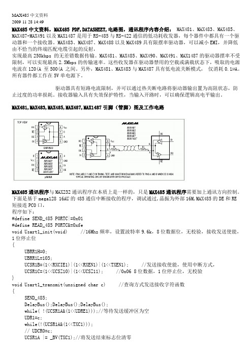
MAX481,MAX483,MAX485,MAX487,MAX1487引脚(管脚)图及工作电路MAX485通讯程序与MAX232通讯程序在本质上是一样的,只是MAX485通讯程序需要加上通讯方向控制。
下面是基于mega128 16AU的485通信中断接收的程序,调试通过,晶振为外部16M,MAX485的DE和RE短接连PC0口,程序如下:#define SEND_485 PORTC|=0x01#define READ_485 PORTC&=0xfevoid Usart1_init(void) //16Mhz频率,设置波特率9.6k,8位数据位,无校验,接收发送使能,1位停止位{UBRR1H=0;UBRR1L=103;UCSR1B=(1<<RXCIE1)|(1<<RXEN1)|(1<<TXEN1); //发送接收使能,使用中断方式,UCSR1C=(1<<UCSZ10)|(1<<UCSZ11); //0x06 8位数据,1位停止位,无校验}void Usart1_transmit(unsigned char c) //查询方式发送接收字符函数{SEND_485;DelayBus();DelayBus();DelayBus();while( !(UCSR1A&(1<<UDRE1)));//等待发送缓冲区为空UDR1=c;while(!(UCSR1A&(1<<TXC1)));// UDCR0=c;UCSR1A |= _BV(TXC1);//将发送结束标志位清零// SET_BIT(UCSR1A,);READ_485;direction++;}SIGNAL(SIG_UART1_RECV)//serial port 1 {if(UCSR1A&(1<<RXC1)){rec1buff=UDR1;rec1_flag=1;。
MEMORY存储芯片MAX488EESA+T中文规格书
±15kV ESD-Protected, Slew-Rate-Limited,Low-Power, RS-485/RS-422 Transceivers__________Function Tables (MAX481E/MAX483E/MAX485E/MAX487E/MAX1487E) Table 1. Transmitting Table 2. Receiving__________Applications Information The MAX481E/MAX483E/MAX485E/MAX487E–MAX491E and MAX1487E are low-power transceivers for RS-485 and RS-422 communications. These “E” versions of the MAX481, MAX483, MAX485, MAX487–MAX491, and MAX1487 provide extra protection against ESD. The rugged MAX481E, MAX483E, MAX485E, MAX497E–MAX491E, and MAX1487E are intended for harsh envi-ronments where high-speed communication is important. These devices eliminate the need for transient suppres-sor diodes and the associated high capacitance loading. The standard (non-“E”) MAX481, MAX483, MAX485, MAX487–MAX491, and MAX1487 are recommended for applications where cost is critical.The MAX481E, MAX485E, MAX490E, MAX491E, and MAX1487E can transmit and receive at data rates up to 2.5Mbps, while the MAX483E, MAX487E, MAX488E, and MAX489E are specified for data rates up to 250kbps. The MAX488E–MAX491E are full-duplex transceivers, while the MAX481E, MAX483E, MAX487E, and MAX1487E are half-duplex. In addition, driver-enable (DE) and receiver-enable (RE) pins are included on the MAX481E, MAX483E, MAX485E, MAX487E, MAX489E, MAX491E, and MAX1487E. When disabled, the driver and receiver outputs are high impedance.±15kV ESD Protection As with all Maxim devices, ESD-protection structures are incorporated on all pins to protect against electro-static discharges encountered during handling and assembly. The driver outputs and receiver inputs have extra protection against static electricity. Maxim’s engi-neers developed state-of-the-art structures to protect these pins against ESD of ±15kV without damage. The ESD structures withstand high ESD in all states: normal operation, shutdown, and powered down. After an ESD event, Maxim’s MAX481E, MAX483E, MAX485E, MAX487E–MAX491E, and MAX1487E keep working without latchup.ESD protection can be tested in various ways; the transmitter outputs and receiver inputs of this product family are characterized for protection to ±15kV using the Human Body Model.Other ESD test methodologies include IEC10004-2 con-tact discharge and IEC1000-4-2 air-gap discharge (for-merly IEC801-2).ESD Test Conditions ESD performance depends on a variety of conditions. Contact Maxim for a reliability report that documents test set-up, test methodology, and test results.Human Body Model F igure 4 shows the Human Body Model, and F igure 5 shows the current waveform it generates when dis-charged into a low impedance. This model consists of a 100pF capacitor charged to the ESD voltage of inter-est, which is then discharged into the test device through a 1.5kΩresistor.IEC1000-4-2 The IEC1000-4-2 standard covers ESD testing and per-formance of finished equipment; it does not specifically refer to integrated circuits (Figure 6).MAX481E/MAX483E/MAX485E/MAX487E–MAX491E/MAX1487E Maxim Integrated9±15kV ESD-Protected, Slew-Rate-Limited, Low-Power, RS-485/RS-422 TransceiversThe major difference between tests done using the Human Body Model and IEC1000-4-2 is higher peak current in IEC1000-4-2, because series resistance is lower in the IEC1000-4-2 model. Hence, the ESD with-stand voltage measured to IEC1000-4-2 is generally lower than that measured using the Human Body Model. Figure 7 shows the current waveform for the 8kV IEC1000-4-2 ESD contact-discharge test.The air-gap test involves approaching the device with a charged probe. The contact-discharge method connects the probe to the device before the probe is energized.Machine Model The Machine Model for ESD tests all pins using a 200pF storage capacitor and zero discharge resis-tance. Its objective is to emulate the stress caused by contact that occurs with handling and assembly during manufacturing. Of course, all pins require this protec-tion during manufacturing—not just inputs and outputs. Therefore,after PC board assembly,the Machine Model is less relevant to I/O ports.MAX487E/MAX1487E:128 Transceivers on the Bus The 48kΩ, 1/4-unit-load receiver input impedance of the MAX487E and MAX1487E allows up to 128 transceivers on a bus, compared to the 1-unit load (12kΩinput impedance) of standard RS-485 drivers (32 transceivers maximum). Any combination of MAX487E/MAX1487E and other RS-485 transceivers with a total of 32 unit loads or less can be put on the bus. The MAX481E, MAX483E, MAX485E, and MAX488E–MAX491E have standard 12kΩreceiver input impedance.MAX483E/MAX487E/MAX488E/MAX489E:Reduced EMI and Reflections The MAX483E and MAX487E–MAX489E are slew-rate limited, minimizing EMI and reducing reflections caused by improperly terminated cables. F igure 16 shows the driver output waveform and its Fourier analy-sis of a 150kHz signal transmitted by a MAX481E, MAX485E, MAX490E, MAX491E, or MAX1487E. High-frequency harmonics with large amplitudes are evident.F igure 17 shows the same information displayed for a MAX483E, MAX487E, MAX488E, or MAX489E transmit-ting under the same conditions. F igure 17’s high-fre-quency harmonics have much lower amplitudes, and the potential for EMI is significantly reduced.Low-Power Shutdown Mode(MAX481E/MAX483E/MAX487E) A low-power shutdown mode is initiated by bringing both RE high and DE low. The devices will not shut down unless both the driver and receiver are disabled. In shutdown, the devices typically draw only 0.5µA of supply current.RE and DE may be driven simultaneously; the parts are guaranteed not to enter shutdown if RE is high and DE is low for less than 50ns. If the inputs are in this state for at least 600ns, the parts are guaranteed to enter shutdown.F or the MAX481E, MAX483E, and MAX487E, the t ZH and t ZL enable times assume the part was not in the low-power shutdown state (the MAX485E, MAX488E–MAX491E, and MAX1487E can not be shut down). The t ZH(SHDN)and t ZL(SHDN)enable times assume the parts were shut down (see Electrical Characteristics).Figure 16. Driver Output Waveform and FFT Plot of MAX485E/MAX490E/MAX491E/MAX1487E Transmitting a 150kHz SignalFigure 17. Driver Output Waveform and FFT Plot ofMAX483E/MAX487E–MAX489E Transmitting a 150kHz SignalMAX481E/MAX483E/MAX485E/ MAX487E–MAX491E/MAX1487E 12。
MAX485EEPA+中文资料

14-Pin Plastic DIP (derate 10.00mW/°C above +70°C) ..800mW 8-Pin SO (derate 5.88mW/°C above +70°C).................471mW 14-Pin SO (derate 8.33mW/°C above +70°C)...............667mW Operating Temperature Ranges MAX4_ _C_ _/MAX1487EC_ A .............................0°C to +70°C MAX4_ _E_ _/MAX1487EE_ A...........................-40°C to +85°C StorageБайду номын сангаасTemperature Range .............................-65°C to +160°C Lead Temperature (soldering, 10sec) .............................+300°C
Receiver Output Voltage (RO)....................-0.5V to (VCC + 0.5V)
Continuous Power Dissipation (TA = +70°C)
8-Pin Plastic DIP (derate 9.09mW/°C above +70°C) ....727mW
Ordering Information
PART MAX481ECPA MAX481ECSA MAX481EEPA MAX481EESA MAX483ECPA MAX483ECSA MAX483EEPA MAX483EESA
MAX4832ETT25C-T中文资料

General DescriptionThe MAX4832/MAX4833 family of low-dropout (LDO)linear regulators feature an accurate current-limiting switch with an integrated FLAG or RESET function. These devices operate from 2.5V to 5.5V and deliver up to 100mA of load current at a preset output voltage. Preset output voltage levels are 1.8V/2.5V/2.8V/3.0V/3.3V.The MAX4832/MAX4833 offer a programmable soft-start control function to eliminate false reset during startup. The MAX4832 provides a FLAG function to noti-fy the system when the load current exceeds the limit.The MAX4833 provides a RESET function to notify the system when the output drops below the threshold.Additionally, reverse-current protection prevents cur-rent flowing from the output to the input. Other features include a low 90µA quiescent current, a 0.1µA shut-down current.The MAX4832/MAX4833 are available in space-saving 6-pin SOT23 and TDFN packages. Each device is speci-fied over the -40°C to +85°C extended temperature range. Contact factory for other programmed output volt-age versions from 1.5V to 3.3V in 100mV increments.For pin-compatible 250mA versions of this device, refer to the MAX4834/MAX4835. For pin-compatible 500mA versions of this device, refer to the MAX4836/MAX4837.ApplicationsSDIO Ports and Devices Notebook Computers USB Ports and Devices Cell Phones PDAs and Palmtop DevicesGPS SystemsFeatures♦Guaranteed Minimum 100mA Load Current♦Accurate Current Limit♦Preset Output Voltages: 1.8V/2.5V/2.8V/3.0V/3.3V ♦2.5V to 5.5V Supply Voltage Range ♦Adjustable Soft-Start ♦Low Dropout Voltage ♦Thermal Shutdown♦Reverse-Current Protection♦Shutdown Output Discharge (MAX4833)♦Low 90µA Supply Current♦Ultra-Low 0.1µA Shutdown Current ♦FLAG and Latch Off (MAX4832) or RESET (MAX4833)♦Tiny SOT23 and TDFN PackagesMAX4832/MAX4833100mA LDO Linear Regulators withCurrent-Limiting Switch________________________________________________________________Maxim Integrated Products1Ordering Information19-3372; Rev 0; 7/04For pricing, delivery, and ordering information,please contact Maxim/Dallas Direct!at 1-888-629-4642, or visit Maxim’s website at .devices. Insert the values found in Table 1 at the end of this doc-ument in the place of “xy”. The “_” is a placeholder for either the RESET or the FLAG feature. Insert “B” in the place of “_” for RESET and “C” for FLAG . “dd” is a placeholder for the reset timeout period. Insert the values found in Table 2 in the place of “dd.” For example, MAX4833EUT18BD2 has a 1.8V output volt-age, RESET feature, and a 30ms reset timeout period. Note that “dd” applies only to the devices with RESET option and does not apply to the devices with FLAG option. For devices with the FLAG option, leave dd blank. Standard versions require a mini-mum order increment of 2.5k units. Nonstandard versions must be ordered in 10k unit increments. Contact factory for availability.*Future product—contact factory for availability.Pin ConfigurationsTables 1 and 2 and Selector Gui de appear at end of data sheet.M A X 4832/M A X 4833100mA LDO Linear Regulators with Current-Limiting SwitchABSOLUTE MAXIMUM RATINGSELECTRICAL CHARACTERISTICSStresses beyond those listed under “Absolute Maximum Ratings” may cause permanent damage to the device. These are stress ratings only, and functional operation of the device at these or any other conditions beyond those indicated in the operational sections of the specifications is not implied. Exposure to absolute maximum rating conditions for extended periods may affect device reliability.IN, SHDN , FLAG , OUT to GND ................................-0.3V to +6V RESET to GND .........................................-0.3V to (V OUT + 0.3V)SS to GND ...................................................-0.3V to (V IN + 0.3V)IN to OUT...............................................................................±6V OUT Short Circuit to GND..........................................Continuous All Pins ESD Handling (Human Body Model).........................2kVContinuous Power Dissipation (T A = +70°C)6-Pin SOT23 (derate 9.1mW/°C above +70°C)................727mW 6-Pin TDFN (derate 24.4mW/°C above +70°C)..........1951.2mW Operating Temperature Range ...........................-40°C to +85°C Operating Junction Temperature Range...........-40°C to +125°C Storage Temperature Range.............................-65°C to +150°C Lead Temperature (soldering, 10s).................................+300°CMAX4832/MAX4833100mA LDO Linear Regulators withCurrent-Limiting Switch_______________________________________________________________________________________3Note 1:Parts are 100% tested at +25°C. Limits across the full temperature range are guaranteed by design and correlation over thespecified temperature range.Note 2:The dropout voltage is measured from V IN to V OUT when V OUT is 2% below its nominal value. The nominal output voltage ismeasured from V OUT to GND when V IN is 1V greater than V OUT . Defined only for V OUT ≥2.5V.Note 3:Soft-start time is defined as the time required for the output to rise from 10% of its nominal value to 90% of its nominal value.Note 4:For V OUT < 2V, V IN must be above 2.5V.Note 5:This is the maximum time OUT can be out of tolerance before a reset is issued. It is implemented to ensure that momentaryoutput glitches do not trigger a reset condition.Note 6:In startup mode, the blanking time counter is not started until the soft-start time has elapsed. The total time from startup toFLAG issued is t SS + t BLANK .ELECTRICAL CHARACTERISTICS (continued)(V IN = V OUT + 1V, SHDN = IN, C OUT = 3.3µF, T A = -40°C to +85°C, unless otherwise noted. Typical values are at T A = +25°C.) (Note 1)M A X 4832/M A X 4833100mA LDO Linear Regulators with Current-Limiting Switch 4_______________________________________________________________________________________Typical Operating Characteristics(V IN = V OUT + 1V, SHDN = IN, C OUT = 3.3µF, T A = +25°C, unless otherwise noted.)QUIESCENT CURRENT vs. INPUT VOLTAGE(NO LOAD)V IN (V)I Q (µA )5432120406080100120006QUIESCENT CURRENT vs. INPUT VOLTAGE(100mA LOAD)V IN (V)I Q (µA )543215010015020025030035006MAXIMUM TRANSIENT DURATION vs. RESET THRESHOLD OVERDRIVERESET THRESHOLD OVERDRIVE (mV)P U L S E D U R A T I O N (µs )1015304560759001100DROPOUT VOLTAGE vs. LOAD CURRENTLOAD CURRENT (mA)D R O P O U T V O L T A GE (m V )806040201020304050607000100POWER-SUPPLY REJECTION RATIOvs. FREQUENCYFREQUENCY (kHz)P S R R (d B )1010.1-70-60-50-40-30-20-100-800.01100REGION OF STABLE C OUT ESRvs. LOAD CURRENTLOAD CURRENT (mA)C O U T E S R (o h m s )90806070203040501012345678910100OUTPUT NOISE vs. FREQUENCYFREQUENCY (Hz)O U T P U T N O I S E (µV R M S )10k1k 1001020304050010100kSOFT-START RESPONSE (C SS = FLOATING)V SS 1V/divV OUT 2V/div V IN 2V/div2ms/divt SS_______________________________________________________________________________________5MAX4832/MAX4833100mA LDO Linear Regulators withCurrent-Limiting SwitchSOFT-START RESPONSE(C SS = 0.01µF)V SS 1V/divV OUT 2V/divV IN 2V/div2ms/divt SSSOFT-START RESPONSE(C SS = 0.1µF)V IN 2V/divV SS 1V/divV OUT 2V/div20ms/divt SSLOAD-TRANSIENT RESPONSEV OUT 50mV/div AC-COUPLED100µs/divV IN = 4.3V V OUT = 3.3V C IN = 0.1µF C OUT = 3.3µFI LOAD : STEP FROM 10mA TO 100mA BACK TO 10mALOAD-TRANSIENT RESPONSENEAR DROPOUTV OUT 50mV/div AC-COUPLED100µs/divV IN = 3.4V V OUT = 3.3V C IN = 0.1µF C OUT = 3.3µFI LOAD : STEP FROM 10mA TO 100mA BACK TO 10mALINE-TRANSIENT RESPONSEV OUT 50mV/div AC-COUPLED100µs/div C IN = 0.1µF C OUT = 3.3µF V OUT = 3.3V I LOAD = 10mA5V V IN500mV/div 4.5V RESET RESPONSE TO V INV RESET 2V/divV OUT 2V/divV IN 2V/div40ms/divt RESETC SS = FLOATINGRESET RESPONSE TO V OUTV RESET 1V/divV OUT 1V/div40ms/div t RESETV IN = 3.5V, C SS = FLOATINGRESET RESPONSE TO SHUTDOWNV RESET 2V/divV OUT 2V/divV SHDN 2V/div40ms/divt RESETV IN = 3.5V, C SS = FLOATINGTypical Operating Characteristics (continued)(V IN = V OUT + 1V, SHDN = IN, C OUT = 3.3µF, T A = +25°C, unless otherwise noted.)M A X 4832/M A X 4833100mA LDO Linear Regulators with Current-Limiting Switch 6_______________________________________________________________________________________Typical Operating Characteristics (continued)(V IN = V OUT + 1V, SHDN = IN, C OUT = 3.3µF, T A = +25°C, unless otherwise noted.)FLAG RESPONSE WHEN OUT IS SHORTED TO GND < BLANKING TIMEMAX4832 toc17V OUT 2V/div 1ms/divI OUT100mA/div V FLAG 2V/divFLAG RESPONSE WHEN OUT IS SHORTED TO GND > BLANKING TIME(IN IS TOGGLED)V OUT 1V/div 10ms/divV IN 2V/divV FLAG 2V/divFLAG CONNECTED TO LOGIC SUPPLYt BLANKSTARTUP IN AN OVERLOAD CONDITION(C SS NOT CONNECTED)V SS 1V/divV FLAG 2V/div V OUT 2V/div2ms/divt BLANKV IN 2V/divt SSV OUT = 2.5VI LOAD = I LIMIT MAXIMUM FLAG CONNECTED TO INSTARTUP IN AN OVERLOAD CONDITION(C SS = 0.01µF)V SS 1V/divV FLAG 2V/divV OUT 2V/div4ms/divt BLANKV IN 2V/divt SSV OUT = 2.5VI LOAD = I LIMIT MAXIMUM FLAG CONNECTED TO INNORMALIZED OUTPUT VOLTAGEvs. TEMPERATURETEMPERATURE (°C)N O R M A L I Z E D O U T P U T V O L T A G E (V )603510-150.9960.9981.0001.0021.0040.994-4085FLAG RESPONSE WHEN OUT IS SHORTED TO GND > BLANKING TIME(SHDN IS TOGGLED)V OUT 1V/div 10ms/divV SHDN 2V/divV FLAG 2V/divFLAG CONNECTED TO LOGIC SUPPLYt BLANKDetailed Description The MAX4832/MAX4833 are ultra-low quiescent current, low-dropout linear regulators with an integrated current limiter. These devices guarantee up to 100mA drive capabilities and regulate the preset output voltage.The MAX4832 has a flag output that asserts low when the load current exceeds the current limit for more than the blanking time (t BLANK). The MAX4833 has a reset output that asserts low when the regulator output volt-age is below the reset threshold voltage (V RESET). V RESET is 87.5% of the nominal output voltage. Figure 1 shows the simplified functional diagram and Figure 2 shows the typical application circuits.FLAG Output (MAX4832) The open-drain FLAG output goes low and the LDO’s pass transistor is latched off when the current in the pass transistor is at its output current limit for more than the blanking time (t BLANK). Cycling IN, or SHDN(high to low to high) brings the device out of its latched-off state and back into normal operation.RESET Output (MAX4833)The RESET output asserts when one of the following conditions occurs:•The input voltage (V IN) is below the input undervolt-age lockout threshold (V UVLO).•The output voltage (V OUT) is below the reset thresh-old (V RESET).•SHDN is pulled low.•The device is in thermal shutdown.•When V OUT> V IN.RESET remains low for the reset timeout period (t RESET)after reset conditions are terminated. There are four RESET timeout periods available as shown in the Electrical Characteristics table. RESET is available in apush-pull configuration as shown in the Selector Guide.ShutdownPull SHDN low to shut down the LDO and reduce the quiescent current consumption of the device from 90µAto 0.1µA. In shutdown mode, the pass transistor, con-trol circuit, and reference circuit are turned off. Connect SHDN to a supply voltage greater than V IH to turn onthe LDO.MAX4832/MAX4833100mA LDO Linear Regulators withCurrent-Limiting Switch _______________________________________________________________________________________7M A X 4832/M A X 4833100mA LDO Linear Regulators with Current-Limiting Switch 8_______________________________________________________________________________________Figure 2. Typical Application CircuitsShutdown Discharge (MAX4833) OUT discharges through a 900Ωinternal resistor during shutdown mode.Reverse OUT to IN Current When the output voltage is greater than the input volt-age, the internal pass transistor turns off. To avoid reverse-charging the input source, the current at IN is guaranteed to be below 3µA when V OUT≥V IN.Current Limit The MAX4832/MAX4833 include an accurate internal current-limiting circuit. OUT can be shorted to ground indefinitely without damaging the part.The MAX4832 latches off if the load current exceeds the current limit for more than the blanking time (see the FLAG Output section). During soft-start, the device does not latch off to an overload condition. During an overload condition, the MAX4833 holds the current at current limit until the thermal limit is reached. Once the junction tem-perature reaches +165°C, thermal shutdown occurs.Thermal Shutdown When the junction temperature (T J) exceeds +165°C, the LDO’s pass transistor turns off allowing the junction to cool. The LDO’s pass transistor turns on again after the IC’s junction temperature cools by 15°C, resulting in a pulsed output during continuous thermal-overload conditions.Soft-Start During power-up, the soft-start ensures that the output ramps up slowly reducing inrush current peaks. See the soft-start response time plots in the Typical Operating Characteristics. The soft-start time (t SS) is given by the following equation:t SS= C SS(ms)where C SS is in nF.A soft-start capacitor (C SS) of 10nF gives a 10ms t SS. A 1ms minimum soft-start time is fixed internally to ensure that the output rises slowly even without any external capacitor at SS pin to ground. The device is in soft-start mode when either the voltage at IN or SHDN is cycled high to low to high.Applications InformationCapacitor Selection and RegulatorStabilityFor stable operation over the full temperature range andwith load currents up to 100mA, use a 3.3µF (min) ceramic output capacitor with an ESR <0.2Ω. To reducenoise and improve load transient response, stability, and power-supply rejection, use larger output capacitor values such as 10µF (note that some ceramic capacitors exhibit large capacitance and ESR variation with temper-ature). X7R capacitors provide good performance overthe -40°C to +85°C operating temperature range.To improve power-supply rejection and transient response, use a 0.1µF capacitor between IN and GND.The MAX4832/MAX4833 remain stable with purely resistive loads or current loads up to 100mA.15kV Operational ESD ProtectionA 3.3µF or higher value ceramic capacitor from OUT toGND provides a 15kV (Human Body Model) protectionat OUT. The ESR value of the capacitor should be lessthan 0.2Ω.Reset Transient ImmunityThe reset circuit is relatively immune to short duration,falling V OUT transients. The Typical Operating Characteristics show a graph of the Maximum Transient Duration vs. Reset Threshold Overdrive for which reset isnot asserted. The graph was produced using falling V OUT transients starting at V OUT and ending below the reset threshold by the magnitude indicated (reset threshold overdrive). The graph shows the maximum pulse widththat a falling V OUT transient can typically have without triggering the reset pulse. As the amplitude of the tran-sient increases (i.e., goes further below the reset thresh-old), the maximum allowable pulse width decreases. Typically, a V OUT transient that goes only 10mV below thereset threshold and lasts up to 54µs does not trigger areset pulse.LayoutWhen using the TDFN package, connect its exposed paddle to G ND to provide a low thermal resistancepath for heat transfer from the IC junction to the printedcircuit board.MAX4832/MAX4833100mA LDO Linear Regulators withCurrent-Limiting Switch _______________________________________________________________________________________9M A X 4832/M A X 4833100mA LDO Linear Regulators with Current-Limiting Switch 10______________________________________________________________________________________Table 1. Standard Output Voltage Suffix 100mV increments. Contact factory for availability.Table 2. R E S E T Timeout Period SuffixPin Configurations (continued)Chip InformationTRANSISTOR COUNT: 1575PROCESS: BiCMOSTDFN Exposed Pad: Connected to GNDMAX4832/MAX4833100mA LDO Linear Regulators withCurrent-Limiting SwitchPackage Information(The package drawing(s) in this data sheet may not reflect the most current specifications. For the latest package outline information go to /packages .)M A X 4832/M A X 4833100mA LDO Linear Regulators with Current-Limiting Switchimplied. Maxim reserves the right to change the circuitry and specifications without notice at any time.12____________________Maxim Integrated Products, 120 San Gabriel Drive, Sunnyvale, CA 94086 408-737-7600©2004 Maxim Integrated ProductsPrinted USAis a registered trademark of Maxim Integrated Products.Package Information (continued)(The package drawing(s) in this data sheet may not reflect the most current specifications. For the latest package outline information go to /packages .)。
高性能热电路断路器483型说明书

Phone: Germany (0 91 87) 10-0 - USA (847) 827-7600 - UK (01296) 420336 - 04/052434DescriptionTypical applicationsTechnical dataSingle pole, miniaturised, aircraft style thermal circuit breaker with tease-free,trip-free, snap action mechanism and push/pull on/off manual actuation (M-type TO CBE to EN 60934). An indicator band on the push button clearly shows the tripped/off position. Threadneck panel mounted, available in metric and US (MS 3320) configurations. Advanced two-chamber design contributes to fail-safe operation. Temperature compensated from -55°to +125 °C, with optional auxiliary contacts, and fully approved for use on a wide range of aircraft and equipment. Full specification ensures suitability for the most demanding applications. For three pole version see type 583.Aircraft systems and equipment (fixed wing and helicopters); other extra low voltage wiring applications; defence equipment; communications systems.483-...without auxiliary contact with auxiliary contactVoltage ratingAC 115 V (400 Hz); DC 28 V(higher voltage ratings upon request)Current rating range 1...35 A Auxiliary circuit 0.5 A, DC 28 V Typical life 20,000 operations mechanical or10,000 operations at I N (≤25 A)5,000 operations at I N (30 + 35 A)Ambient temperature -55...+125 °C (-67...+257 °F)Insulation co-ordination rated impulse pollution (IEC 60664 and 60664A) withstand voltage degree1.5 kV 3Dielectric strength(IEC 60664 and 60664A) test voltage operating area AC 1,500 V main to aux. circuit AC 1,500 V Insulation resistance >100 M Ω(DC 500 V)Interrupting capacity I cn AC 115 V (400 Hz):≤4 A 1,000 A 5 A 2,000 A 7.5...35 A 2,500 A DC 28 V:1...25 A 6,000 A 30 + 35 A 4,000 ADegree of protection operating area IP40 (IEC 60529/DIN 40050)terminal area IP00Vibration (sinusoidal) 15 g (70-2000 Hz) ±0.76 mm (5-70 Hz)to VG 95210, sheet 19/IEC 60068-2-6, test Fc/ISO 7137Vibration (random) 16.4 g rms, 0.2 g 2/Hz ±1.5 dBto VG 95210, sheet 29/ISO 7137Acceleration 17 g, to ISO 2669Shock 75 g (11 ms) to VG 95210, sheet 28/IEC 60068-2-27, test Ea/ISO 7137Corrosion 96 hours at 5 % salt mist, severity A48 hours at 20 % salt mist, severity B to VG 95210, sheet 2/IEC 60068-2-11, test Ka/ISO 7137Humidity 240 hours at 95 % RH,to VG 95210, sheet 7/IEC 60068-2-3, test C/ISO 7137Explosion to VG 95210, sheet 10/MIL-STD-202, meth. 109Altitude ≤25,000 m above sea level Mass max. 29 g with auxiliary contactmax. 25 g without auxiliary contactWeight reduction through aluminium threadneck: approx. 3 g ApprovalsAuthority Voltage ratingsCurrent ratingsLN 29886VG 95345 T06MS 3320, MS 3320 V QPL ULDC 75 V 1...35 AStandard current ratings and typical volt drop valuesCurrentVolt dropCurrent Volt drop rating (A)(mV)rating (A)(mV)1750101902520151902.5400202003360251704350301605260351507.5230All dimensions without tolerances are for reference only. In the interest of improved design,performance and cost effectiveness the right to make changes in these specifications without notice is reserved.Product markings may not be exactly as the ordering codes.Errors and omissions excepted.。
MAX488ESA-T中文资料

For pricing, delivery, and ordering information,please contact Maxim/Dallas Direct!at 1-888-629-4642, or visit Maxim’s website at .General DescriptionThe MAX481, MAX483, MAX485, MAX487–MAX491, and MAX1487 are low-power transceivers for RS-485 and RS-422 communication. Each part contains one driver and one receiver. The MAX483, MAX487, MAX488, and MAX489feature reduced slew-rate drivers that minimize EMI and reduce reflections caused by improperly terminated cables,thus allowing error-free data transmission up to 250kbps.The driver slew rates of the MAX481, MAX485, MAX490,MAX491, and MAX1487 are not limited, allowing them to transmit up to 2.5Mbps.These transceivers draw between 120µA and 500µA of supply current when unloaded or fully loaded with disabled drivers. Additionally, the MAX481, MAX483, and MAX487have a low-current shutdown mode in which they consume only 0.1µA. All parts operate from a single 5V supply.Drivers are short-circuit current limited and are protected against excessive power dissipation by thermal shutdown circuitry that places the driver outputs into a high-imped-ance state. The receiver input has a fail-safe feature that guarantees a logic-high output if the input is open circuit.The MAX487 and MAX1487 feature quarter-unit-load receiver input impedance, allowing up to 128 MAX487/MAX1487 transceivers on the bus. Full-duplex communi-cations are obtained using the MAX488–MAX491, while the MAX481, MAX483, MAX485, MAX487, and MAX1487are designed for half-duplex applications.________________________ApplicationsLow-Power RS-485 Transceivers Low-Power RS-422 Transceivers Level TranslatorsTransceivers for EMI-Sensitive Applications Industrial-Control Local Area Networks__Next Generation Device Features♦For Fault-Tolerant ApplicationsMAX3430: ±80V Fault-Protected, Fail-Safe, 1/4Unit Load, +3.3V, RS-485 TransceiverMAX3440E–MAX3444E: ±15kV ESD-Protected,±60V Fault-Protected, 10Mbps, Fail-Safe, RS-485/J1708 Transceivers♦For Space-Constrained ApplicationsMAX3460–MAX3464: +5V, Fail-Safe, 20Mbps,Profibus RS-485/RS-422 TransceiversMAX3362: +3.3V, High-Speed, RS-485/RS-422Transceiver in a SOT23 PackageMAX3280E–MAX3284E: ±15kV ESD-Protected,52Mbps, +3V to +5.5V, SOT23, RS-485/RS-422,True Fail-Safe ReceiversMAX3293/MAX3294/MAX3295: 20Mbps, +3.3V,SOT23, RS-855/RS-422 Transmitters ♦For Multiple Transceiver ApplicationsMAX3030E–MAX3033E: ±15kV ESD-Protected,+3.3V, Quad RS-422 Transmitters ♦For Fail-Safe ApplicationsMAX3080–MAX3089: Fail-Safe, High-Speed (10Mbps), Slew-Rate-Limited RS-485/RS-422Transceivers♦For Low-Voltage ApplicationsMAX3483E/MAX3485E/MAX3486E/MAX3488E/MAX3490E/MAX3491E: +3.3V Powered, ±15kV ESD-Protected, 12Mbps, Slew-Rate-Limited,True RS-485/RS-422 TransceiversMAX481/MAX483/MAX485/MAX487–MAX491/MAX1487Low-Power, Slew-Rate-Limited RS-485/RS-422 Transceivers______________________________________________________________Selection Table19-0122; Rev 8; 10/03Ordering Information appears at end of data sheet.M A X 481/M A X 483/M A X 485/M A X 487–M A X 491/M A X 1487Low-Power, Slew-Rate-Limited RS-485/RS-422 Transceivers 2_______________________________________________________________________________________ABSOLUTE MAXIMUM RATINGSSupply Voltage (V CC ).............................................................12V Control Input Voltage (RE , DE)...................-0.5V to (V CC + 0.5V)Driver Input Voltage (DI).............................-0.5V to (V CC + 0.5V)Driver Output Voltage (A, B)...................................-8V to +12.5V Receiver Input Voltage (A, B).................................-8V to +12.5V Receiver Output Voltage (RO).....................-0.5V to (V CC +0.5V)Continuous Power Dissipation (T A = +70°C)8-Pin Plastic DIP (derate 9.09mW/°C above +70°C)....727mW 14-Pin Plastic DIP (derate 10.00mW/°C above +70°C)..800mW 8-Pin SO (derate 5.88mW/°C above +70°C).................471mW14-Pin SO (derate 8.33mW/°C above +70°C)...............667mW 8-Pin µMAX (derate 4.1mW/°C above +70°C)..............830mW 8-Pin CERDIP (derate 8.00mW/°C above +70°C).........640mW 14-Pin CERDIP (derate 9.09mW/°C above +70°C).......727mW Operating Temperature RangesMAX4_ _C_ _/MAX1487C_ A...............................0°C to +70°C MAX4__E_ _/MAX1487E_ A.............................-40°C to +85°C MAX4__MJ_/MAX1487MJA...........................-55°C to +125°C Storage Temperature Range.............................-65°C to +160°C Lead Temperature (soldering, 10sec).............................+300°CDC ELECTRICAL CHARACTERISTICS(V CC = 5V ±5%, T A = T MIN to T MAX , unless otherwise noted.) (Notes 1, 2)Stresses beyond those listed under “Absolute Maximum Ratings” may cause permanent damage to the device. These are stress ratings only, and functional operation of the device at these or any other conditions beyond those indicated in the operational sections of the specifications is not implied. Exposure to absolute maximum rating conditions for extended periods may affect device reliability.V V IN = -7VV IN = 12V V IN = -7V V IN = 12V Input Current (A, B)I IN2V TH k Ω48-7V ≤V CM ≤12V, MAX487/MAX1487R INReceiver Input Resistance -7V ≤V CM ≤12V, all devices except MAX487/MAX1487R = 27Ω(RS-485), Figure 40.4V ≤V O ≤2.4VR = 50Ω(RS-422)I O = 4mA, V ID = -200mV I O = -4mA, V ID = 200mV V CM = 0V-7V ≤V CM ≤12V DE, DI, RE DE, DI, RE MAX487/MAX1487,DE = 0V, V CC = 0V or 5.25VDE, DI, RE R = 27Ωor 50Ω, Figure 4R = 27Ωor 50Ω, Figure 4R = 27Ωor 50Ω, Figure 4DE = 0V;V CC = 0V or 5.25V,all devices except MAX487/MAX1487CONDITIONSk Ω12µA ±1I OZRThree-State (high impedance)Output Current at ReceiverV 0.4V OL Receiver Output Low Voltage 3.5V OH Receiver Output High Voltage mV 70∆V TH Receiver Input Hysteresis V -0.20.2Receiver Differential Threshold Voltage-0.2mA 0.25mA-0.81.01.55V OD2Differential Driver Output (with load)V 2V 5V OD1Differential Driver Output (no load)µA±2I IN1Input CurrentV 0.8V IL Input Low Voltage V 2.0V IH Input High Voltage V 0.2∆V OD Change in Magnitude of Driver Common-Mode Output Voltage for Complementary Output States V 0.2∆V OD Change in Magnitude of Driver Differential Output Voltage for Complementary Output States V 3V OC Driver Common-Mode Output VoltageUNITS MINTYPMAX SYMBOL PARAMETERMAX481/MAX483/MAX485/MAX487–MAX491/MAX1487Low-Power, Slew-Rate-Limited RS-485/RS-422 Transceivers_______________________________________________________________________________________3SWITCHING CHARACTERISTICS—MAX481/MAX485, MAX490/MAX491, MAX1487(V CC = 5V ±5%, T A = T MIN to T MAX , unless otherwise noted.) (Notes 1, 2)DC ELECTRICAL CHARACTERISTICS (continued)(V CC = 5V ±5%, T A = T MIN to T MAX , unless otherwise noted.) (Notes 1, 2)ns 103060t PHLDriver Rise or Fall Time Figures 6 and 8, R DIFF = 54Ω, C L1= C L2= 100pF ns MAX490M, MAX491M MAX490C/E, MAX491C/E2090150MAX481, MAX485, MAX1487MAX490M, MAX491MMAX490C/E, MAX491C/E MAX481, MAX485, MAX1487Figures 6 and 8, R DIFF = 54Ω,C L1= C L2= 100pF MAX481 (Note 5)Figures 5 and 11, C RL = 15pF, S2 closedFigures 5 and 11, C RL = 15pF, S1 closed Figures 5 and 11, C RL = 15pF, S2 closed Figures 5 and 11, C RL = 15pF, S1 closed Figures 6 and 10, R DIFF = 54Ω,C L1= C L2= 100pFFigures 6 and 8,R DIFF = 54Ω,C L1= C L2= 100pF Figures 6 and 10,R DIFF = 54Ω,C L1= C L2= 100pF CONDITIONS ns 510t SKEW ns50200600t SHDNTime to ShutdownMbps 2.5f MAX Maximum Data Rate ns 2050t HZ Receiver Disable Time from High ns 103060t PLH 2050t LZ Receiver Disable Time from Low ns 2050t ZH Driver Input to Output Receiver Enable to Output High ns 2050t ZL Receiver Enable to Output Low 2090200ns ns 134070t HZ t SKD Driver Disable Time from High |t PLH - t PHL |DifferentialReceiver Skewns 4070t LZ Driver Disable Time from Low ns 4070t ZL Driver Enable to Output Low 31540ns51525ns 31540t R , t F 2090200Driver Output Skew to Output t PLH , t PHL Receiver Input to Output4070t ZH Driver Enable to Output High UNITS MIN TYP MAX SYMBOL PARAMETERFigures 7 and 9, C L = 100pF, S2 closed Figures 7 and 9, C L = 100pF, S1 closed Figures 7 and 9, C L = 15pF, S1 closed Figures 7 and 9, C L = 15pF, S2 closedM A X 481/M A X 483/M A X 485/M A X 487–M A X 491/M A X 1487Low-Power, Slew-Rate-Limited RS-485/RS-422 Transceivers 4_______________________________________________________________________________________SWITCHING CHARACTERISTICS—MAX483, MAX487/MAX488/MAX489(V CC = 5V ±5%, T A = T MIN to T MAX , unless otherwise noted.) (Notes 1, 2)SWITCHING CHARACTERISTICS—MAX481/MAX485, MAX490/MAX491, MAX1487 (continued)(V CC = 5V ±5%, T A = T MIN to T MAX , unless otherwise noted.) (Notes 1, 2)3001000Figures 7 and 9, C L = 100pF, S2 closed Figures 7 and 9, C L = 100pF, S1 closed Figures 5 and 11, C L = 15pF, S2 closed,A - B = 2VCONDITIONSns 40100t ZH(SHDN)Driver Enable from Shutdown toOutput High (MAX481)nsFigures 5 and 11, C L = 15pF, S1 closed,B - A = 2Vt ZL(SHDN)Receiver Enable from Shutdownto Output Low (MAX481)ns 40100t ZL(SHDN)Driver Enable from Shutdown toOutput Low (MAX481)ns 3001000t ZH(SHDN)Receiver Enable from Shutdownto Output High (MAX481)UNITS MINTYP MAX SYMBOLPARAMETERt PLH t SKEW Figures 6 and 8, R DIFF = 54Ω,C L1= C L2= 100pFt PHL Figures 6 and 8, R DIFF = 54Ω,C L1= C L2= 100pFDriver Input to Output Driver Output Skew to Output ns 100800ns ns 2000MAX483/MAX487, Figures 7 and 9,C L = 100pF, S2 closedt ZH(SHDN)Driver Enable from Shutdown to Output High2502000ns2500MAX483/MAX487, Figures 5 and 11,C L = 15pF, S1 closedt ZL(SHDN)Receiver Enable from Shutdown to Output Lowns 2500MAX483/MAX487, Figures 5 and 11,C L = 15pF, S2 closedt ZH(SHDN)Receiver Enable from Shutdown to Output Highns 2000MAX483/MAX487, Figures 7 and 9,C L = 100pF, S1 closedt ZL(SHDN)Driver Enable from Shutdown to Output Lowns 50200600MAX483/MAX487 (Note 5) t SHDN Time to Shutdownt PHL t PLH , t PHL < 50% of data period Figures 5 and 11, C RL = 15pF, S2 closed Figures 5 and 11, C RL = 15pF, S1 closed Figures 5 and 11, C RL = 15pF, S2 closed Figures 5 and 11, C RL = 15pF, S1 closed Figures 7 and 9, C L = 15pF, S2 closed Figures 6 and 10, R DIFF = 54Ω,C L1= C L2= 100pFFigures 7 and 9, C L = 15pF, S1 closed Figures 7 and 9, C L = 100pF, S1 closed Figures 7 and 9, C L = 100pF, S2 closed CONDITIONSkbps 250f MAX 2508002000Maximum Data Rate ns 2050t HZ Receiver Disable Time from High ns 25080020002050t LZ Receiver Disable Time from Low ns 2050t ZH Receiver Enable to Output High ns 2050t ZL Receiver Enable to Output Low ns ns 1003003000t HZ t SKD Driver Disable Time from High I t PLH - t PHL I DifferentialReceiver SkewFigures 6 and 10, R DIFF = 54Ω,C L1= C L2= 100pFns 3003000t LZ Driver Disable Time from Low ns 2502000t ZL Driver Enable to Output Low ns Figures 6 and 8, R DIFF = 54Ω,C L1= C L2= 100pFns 2502000t R , t F 2502000Driver Rise or Fall Time ns t PLH Receiver Input to Output2502000t ZH Driver Enable to Output High UNITS MIN TYP MAX SYMBOL PARAMETERMAX481/MAX483/MAX485/MAX487–MAX491/MAX1487Low-Power, Slew-Rate-Limited RS-485/RS-422 Transceivers_______________________________________________________________________________________530002.5OUTPUT CURRENT vs.RECEIVER OUTPUT LOW VOLTAGE525M A X 481-01OUTPUT LOW VOLTAGE (V)O U T P U T C U R R E N T (m A )1.515100.51.02.0203540450.90.1-50-252575RECEIVER OUTPUT LOW VOLTAGE vs.TEMPERATURE0.30.7TEMPERATURE (°C)O U T P U TL O W V O L T A G E (V )500.50.80.20.60.40100125-20-41.5 2.0 3.0 5.0OUTPUT CURRENT vs.RECEIVER OUTPUT HIGH VOLTAGE-8-16M A X 481-02OUTPUT HIGH VOLTAGE (V)O U T P U T C U R R E N T (m A )2.5 4.0-12-18-6-14-10-203.54.5 4.83.2-50-252575RECEIVER OUTPUT HIGH VOLTAGE vs.TEMPERATURE3.64.4TEMPERATURE (°C)O U T P UT H I G H V O L T A G E (V )0504.04.63.44.23.83.01001259000 1.0 3.0 4.5DRIVER OUTPUT CURRENT vs.DIFFERENTIAL OUTPUT VOLTAGE1070M A X 481-05DIFFERENTIAL OUTPUT VOLTAGE (V)O U T P U T C U R R E N T (m A )2.0 4.05030806040200.5 1.5 2.53.5 2.31.5-50-2525125DRIVER DIFFERENTIAL OUTPUT VOLTAGEvs. TEMPERATURE1.72.1TEMPERATURE (°C)D I F FE R E N T I A L O U T P U T V O L T A G E (V )751.92.21.62.01.8100502.4__________________________________________Typical Operating Characteristics(V CC = 5V, T A = +25°C, unless otherwise noted.)NOTES FOR ELECTRICAL/SWITCHING CHARACTERISTICSNote 1:All currents into device pins are positive; all currents out of device pins are negative. All voltages are referenced to deviceground unless otherwise specified.Note 2:All typical specifications are given for V CC = 5V and T A = +25°C.Note 3:Supply current specification is valid for loaded transmitters when DE = 0V.Note 4:Applies to peak current. See Typical Operating Characteristics.Note 5:The MAX481/MAX483/MAX487 are put into shutdown by bringing RE high and DE low. If the inputs are in this state for lessthan 50ns, the parts are guaranteed not to enter shutdown. If the inputs are in this state for at least 600ns, the parts are guaranteed to have entered shutdown. See Low-Power Shutdown Mode section.M A X 481/M A X 483/M A X 485/M A X 487–M A X 491/M A X 1487Low-Power, Slew-Rate-Limited RS-485/RS-422 Transceivers 6___________________________________________________________________________________________________________________Typical Operating Characteristics (continued)(V CC = 5V, T A = +25°C, unless otherwise noted.)120008OUTPUT CURRENT vs.DRIVER OUTPUT LOW VOLTAGE20100M A X 481-07OUTPUT LOW VOLTAGE (V)O U T P U T C U R R E N T (m A )6604024801012140-1200-7-5-15OUTPUT CURRENT vs.DRIVER OUTPUT HIGH VOLTAGE-20-80M A X 481-08OUTPUT HIGH VOLTAGE (V)O U T P U T C U R R E N T (m A )-31-603-6-4-2024-100-40100-40-60-2040100120MAX1487SUPPLY CURRENT vs. TEMPERATURE300TEMPERATURE (°C)S U P P L Y C U R R E N T (µA )20608050020060040000140100-50-2550100MAX481/MAX485/MAX490/MAX491SUPPLY CURRENT vs. TEMPERATURE300TEMPERATURE (°C)S U P P L Y C U R R E N T (µA )257550020060040000125100-50-2550100MAX483/MAX487–MAX489SUPPLY CURRENT vs. TEMPERATURE300TEMPERATURE (°C)S U P P L Y C U R R E N T (µA )257550020060040000125MAX481/MAX483/MAX485/MAX487–MAX491/MAX1487Low-Power, Slew-Rate-Limited RS-485/RS-422 Transceivers_______________________________________________________________________________________7______________________________________________________________Pin DescriptionFigure 1. MAX481/MAX483/MAX485/MAX487/MAX1487 Pin Configuration and Typical Operating CircuitM A X 481/M A X 483/M A X 485/M A X 487–M A X 491/M A X 1487__________Applications InformationThe MAX481/MAX483/MAX485/MAX487–MAX491 and MAX1487 are low-power transceivers for RS-485 and RS-422 communications. The MAX481, MAX485, MAX490,MAX491, and MAX1487 can transmit and receive at data rates up to 2.5Mbps, while the MAX483, MAX487,MAX488, and MAX489 are specified for data rates up to 250kbps. The MAX488–MAX491 are full-duplex trans-ceivers while the MAX481, MAX483, MAX485, MAX487,and MAX1487 are half-duplex. In addition, Driver Enable (DE) and Receiver Enable (RE) pins are included on the MAX481, MAX483, MAX485, MAX487, MAX489,MAX491, and MAX1487. When disabled, the driver and receiver outputs are high impedance.MAX487/MAX1487:128 Transceivers on the BusThe 48k Ω, 1/4-unit-load receiver input impedance of the MAX487 and MAX1487 allows up to 128 transceivers on a bus, compared to the 1-unit load (12k Ωinput impedance) of standard RS-485 drivers (32 trans-ceivers maximum). Any combination of MAX487/MAX1487 and other RS-485 transceivers with a total of 32 unit loads or less can be put on the bus. The MAX481/MAX483/MAX485 and MAX488–MAX491 have standard 12k ΩReceiver Input impedance.Low-Power, Slew-Rate-Limited RS-485/RS-422 Transceivers 8_______________________________________________________________________________________Figure 2. MAX488/MAX490 Pin Configuration and Typical Operating CircuitFigure 3. MAX489/MAX491 Pin Configuration and Typical Operating CircuitMAX483/MAX487/MAX488/MAX489:Reduced EMI and ReflectionsThe MAX483 and MAX487–MAX489 are slew-rate limit-ed, minimizing EMI and reducing reflections caused by improperly terminated cables. Figure 12 shows the dri-ver output waveform and its Fourier analysis of a 150kHz signal transmitted by a MAX481, MAX485,MAX490, MAX491, or MAX1487. High-frequency har-monics with large amplitudes are evident. Figure 13shows the same information displayed for a MAX483,MAX487, MAX488, or MAX489 transmitting under the same conditions. Figure 13’s high-frequency harmonics have much lower amplitudes, and the potential for EMI is significantly reduced.MAX481/MAX483/MAX485/MAX487–MAX491/MAX1487Low-Power, Slew-Rate-Limited RS-485/RS-422 Transceivers_______________________________________________________________________________________9_________________________________________________________________Test CircuitsFigure 4. Driver DC Test Load Figure 5. Receiver Timing Test LoadFigure 6. Driver/Receiver Timing Test Circuit Figure 7. Driver Timing Test LoadM A X 481/M A X 483/M A X 485/M A X 487–M A X 491/M A X 1487Low-Power, Slew-Rate-Limited RS-485/RS-422 Transceivers 10_______________________________________________________Switching Waveforms_________________Function Tables (MAX481/MAX483/MAX485/MAX487/MAX1487)Figure 8. Driver Propagation DelaysFigure 9. Driver Enable and Disable Times (except MAX488 and MAX490)Figure 10. Receiver Propagation DelaysFigure 11. Receiver Enable and Disable Times (except MAX488and MAX490)Table 1. TransmittingTable 2. ReceivingLow-Power Shutdown Mode (MAX481/MAX483/MAX487)A low-power shutdown mode is initiated by bringing both RE high and DE low. The devices will not shut down unless both the driver and receiver are disabled.In shutdown, the devices typically draw only 0.1µA of supply current.RE and DE may be driven simultaneously; the parts are guaranteed not to enter shutdown if RE is high and DE is low for less than 50ns. If the inputs are in this state for at least 600ns, the parts are guaranteed to enter shutdown.For the MAX481, MAX483, and MAX487, the t ZH and t ZL enable times assume the part was not in the low-power shutdown state (the MAX485/MAX488–MAX491and MAX1487 can not be shut down). The t ZH(SHDN)and t ZL(SHDN)enable times assume the parts were shut down (see Electrical Characteristics ).It takes the drivers and receivers longer to become enabled from the low-power shutdown state (t ZH(SHDN ), t ZL(SHDN)) than from the operating mode (t ZH , t ZL ). (The parts are in operating mode if the –R —E –,DE inputs equal a logical 0,1 or 1,1 or 0, 0.)Driver Output ProtectionExcessive output current and power dissipation caused by faults or by bus contention are prevented by two mechanisms. A foldback current limit on the output stage provides immediate protection against short cir-cuits over the whole common-mode voltage range (see Typical Operating Characteristics ). In addition, a ther-mal shutdown circuit forces the driver outputs into a high-impedance state if the die temperature rises excessively.Propagation DelayMany digital encoding schemes depend on the differ-ence between the driver and receiver propagation delay times. Typical propagation delays are shown in Figures 15–18 using Figure 14’s test circuit.The difference in receiver delay times, | t PLH - t PHL |, is typically under 13ns for the MAX481, MAX485,MAX490, MAX491, and MAX1487 and is typically less than 100ns for the MAX483 and MAX487–MAX489.The driver skew times are typically 5ns (10ns max) for the MAX481, MAX485, MAX490, MAX491, and MAX1487, and are typically 100ns (800ns max) for the MAX483 and MAX487–MAX489.MAX481/MAX483/MAX485/MAX487–MAX491/MAX1487Low-Power, Slew-Rate-Limited RS-485/RS-422 Transceivers______________________________________________________________________________________1110dB/div0Hz5MHz500kHz/div10dB/div0Hz5MHz500kHz/divFigure 12. Driver Output Waveform and FFT Plot of MAX481/MAX485/MAX490/MAX491/MAX1487 Transmitting a 150kHz SignalFigure 13. Driver Output Waveform and FFT Plot of MAX483/MAX487–MAX489 Transmitting a 150kHz SignalM A X 481/M A X 483/M A X 485/M A X 487–M A X 491/M A X 1487Low-Power, Slew-Rate-Limited RS-485/RS-422 Transceivers 12______________________________________________________________________________________V CC = 5V T A = +25°CV CC = 5V T A = +25°CV CC = 5V T A = +25°CV CC = 5V T A = +25°CFigure 14. Receiver Propagation Delay Test CircuitFigure 15. MAX481/MAX485/MAX490/MAX491/MAX1487Receiver t PHLFigure 16. MAX481/MAX485/MAX490/MAX491/MAX1487Receiver t PLHPHL Figure 18. MAX483, MAX487–MAX489 Receiver t PLHLine Length vs. Data RateThe RS-485/RS-422 standard covers line lengths up to 4000 feet. For line lengths greater than 4000 feet, see Figure 23.Figures 19 and 20 show the system differential voltage for the parts driving 4000 feet of 26AWG twisted-pair wire at 110kHz into 120Ωloads.Typical ApplicationsThe MAX481, MAX483, MAX485, MAX487–MAX491, and MAX1487 transceivers are designed for bidirectional data communications on multipoint bus transmission lines.Figures 21 and 22 show typical network applications circuits. These parts can also be used as line repeaters, with cable lengths longer than 4000 feet, as shown in Figure 23.To minimize reflections, the line should be terminated at both ends in its characteristic impedance, and stub lengths off the main line should be kept as short as possi-ble. The slew-rate-limited MAX483 and MAX487–MAX489are more tolerant of imperfect termination.MAX481/MAX483/MAX485/MAX487–MAX491/MAX1487Low-Power, Slew-Rate-Limited RS-485/RS-422 Transceivers______________________________________________________________________________________13DIV Y -V ZRO5V 0V1V0V -1V5V 0V2µs/divFigure 19. MAX481/MAX485/MAX490/MAX491/MAX1487 System Differential Voltage at 110kHz Driving 4000ft of Cable Figure 20. MAX483, MAX487–MAX489 System Differential Voltage at 110kHz Driving 4000ft of CableFigure 21. MAX481/MAX483/MAX485/MAX487/MAX1487 Typical Half-Duplex RS-485 NetworkM A X 481/M A X 483/M A X 485/M A X 487–M A X 491/M A X 1487Low-Power, Slew-Rate-Limited RS-485/RS-422 Transceivers 14______________________________________________________________________________________Figure 22. MAX488–MAX491 Full-Duplex RS-485 NetworkFigure 23. Line Repeater for MAX488–MAX491Isolated RS-485For isolated RS-485 applications, see the MAX253 and MAX1480 data sheets.MAX481/MAX483/MAX485/MAX487–MAX491/MAX1487Low-Power, Slew-Rate-Limited RS-485/RS-422 Transceivers______________________________________________________________________________________15_______________Ordering Information_________________Chip TopographiesMAX481/MAX483/MAX485/MAX487/MAX1487N.C. RO 0.054"(1.372mm)0.080"(2.032mm)DE DIGND B N.C.V CCARE * Contact factory for dice specifications.__Ordering Information (continued)M A X 481/M A X 483/M A X 485/M A X 487–M A X 491/M A X 1487Low-Power, Slew-Rate-Limited RS-485/RS-422 Transceivers 16______________________________________________________________________________________TRANSISTOR COUNT: 248SUBSTRATE CONNECTED TO GNDMAX488/MAX490B RO 0.054"(1.372mm)0.080"(2.032mm)N.C. DIGND Z A V CCYN.C._____________________________________________Chip Topographies (continued)MAX489/MAX491B RO 0.054"(1.372mm)0.080"(2.032mm)DE DIGND Z A V CCYREMAX481/MAX483/MAX485/MAX487–MAX491/MAX1487Low-Power, Slew-Rate-Limited RS-485/RS-422 Transceivers______________________________________________________________________________________17Package Information(The package drawing(s) in this data sheet may not reflect the most current specifications. For the latest package outline information go to /packages .)S O I C N .E P SM A X 481/M A X 483/M A X 485/M A X 487–M A X 491/M A X 1487Low-Power, Slew-Rate-Limited RS-485/RS-422 Transceivers 18______________________________________________________________________________________Package Information (continued)(The package drawing(s) in this data sheet may not reflect the most current specifications. For the latest package outline information go to /packages .)MAX481/MAX483/MAX485/MAX487–MAX491Low-Power, Slew-Rate-Limited RS-485/RS-422 TransceiversMaxim cannot assume responsibility for use of any circuitry other than circuitry entirely embodied in a Maxim product. No circuit patent licenses are implied. Maxim reserves the right to change the circuitry and specifications without notice at any time.Maxim Integrated Products, 120 San Gabriel Drive, Sunnyvale, CA 94086 408-737-7600 ____________________19©2003 Maxim Integrated ProductsPrinted USAis a registered trademark of Maxim Integrated Products.M A X 481/M A X 483/M A X 485/M A X 487–M A X 491/M A X 1487P D I P N .E PSPackage Information (continued)(The package drawing(s) in this data sheet may not reflect the most current specifications. For the latest package outline information go to /packages .)。
- 1、下载文档前请自行甄别文档内容的完整性,平台不提供额外的编辑、内容补充、找答案等附加服务。
- 2、"仅部分预览"的文档,不可在线预览部分如存在完整性等问题,可反馈申请退款(可完整预览的文档不适用该条件!)。
- 3、如文档侵犯您的权益,请联系客服反馈,我们会尽快为您处理(人工客服工作时间:9:00-18:30)。
For pricing, delivery, and ordering information,please contact Maxim/Dallas Direct!at 1-888-629-4642, or visit Maxim’s website at .General DescriptionThe MAX481, MAX483, MAX485, MAX487–MAX491, and MAX1487 are low-power transceivers for RS-485 and RS-422 communication. Each part contains one driver and one receiver. The MAX483, MAX487, MAX488, and MAX489feature reduced slew-rate drivers that minimize EMI and reduce reflections caused by improperly terminated cables,thus allowing error-free data transmission up to 250kbps.The driver slew rates of the MAX481, MAX485, MAX490,MAX491, and MAX1487 are not limited, allowing them to transmit up to 2.5Mbps.These transceivers draw between 120µA and 500µA of supply current when unloaded or fully loaded with disabled drivers. Additionally, the MAX481, MAX483, and MAX487have a low-current shutdown mode in which they consume only 0.1µA. All parts operate from a single 5V supply.Drivers are short-circuit current limited and are protected against excessive power dissipation by thermal shutdown circuitry that places the driver outputs into a high-imped-ance state. The receiver input has a fail-safe feature that guarantees a logic-high output if the input is open circuit.The MAX487 and MAX1487 feature quarter-unit-load receiver input impedance, allowing up to 128 MAX487/MAX1487 transceivers on the bus. Full-duplex communi-cations are obtained using the MAX488–MAX491, while the MAX481, MAX483, MAX485, MAX487, and MAX1487are designed for half-duplex applications.________________________ApplicationsLow-Power RS-485 Transceivers Low-Power RS-422 Transceivers Level TranslatorsTransceivers for EMI-Sensitive Applications Industrial-Control Local Area Networks__Next Generation Device Features♦For Fault-Tolerant ApplicationsMAX3430: ±80V Fault-Protected, Fail-Safe, 1/4Unit Load, +3.3V, RS-485 TransceiverMAX3440E–MAX3444E: ±15kV ESD-Protected,±60V Fault-Protected, 10Mbps, Fail-Safe, RS-485/J1708 Transceivers♦For Space-Constrained ApplicationsMAX3460–MAX3464: +5V, Fail-Safe, 20Mbps,Profibus RS-485/RS-422 TransceiversMAX3362: +3.3V, High-Speed, RS-485/RS-422Transceiver in a SOT23 PackageMAX3280E–MAX3284E: ±15kV ESD-Protected,52Mbps, +3V to +5.5V, SOT23, RS-485/RS-422,True Fail-Safe ReceiversMAX3293/MAX3294/MAX3295: 20Mbps, +3.3V,SOT23, RS-855/RS-422 Transmitters ♦For Multiple Transceiver ApplicationsMAX3030E–MAX3033E: ±15kV ESD-Protected,+3.3V, Quad RS-422 Transmitters ♦For Fail-Safe ApplicationsMAX3080–MAX3089: Fail-Safe, High-Speed (10Mbps), Slew-Rate-Limited RS-485/RS-422Transceivers♦For Low-Voltage ApplicationsMAX3483E/MAX3485E/MAX3486E/MAX3488E/MAX3490E/MAX3491E: +3.3V Powered, ±15kV ESD-Protected, 12Mbps, Slew-Rate-Limited,True RS-485/RS-422 TransceiversMAX481/MAX483/MAX485/MAX487–MAX491/MAX1487Low-Power, Slew-Rate-Limited RS-485/RS-422 Transceivers______________________________________________________________Selection Table19-0122; Rev 8; 10/03Ordering Information appears at end of data sheet.M A X 481/M A X 483/M A X 485/M A X 487–M A X 491/M A X 1487Low-Power, Slew-Rate-Limited RS-485/RS-422 Transceivers 2_______________________________________________________________________________________ABSOLUTE MAXIMUM RATINGSSupply Voltage (V CC ).............................................................12V Control Input Voltage (RE , DE)...................-0.5V to (V CC + 0.5V)Driver Input Voltage (DI).............................-0.5V to (V CC + 0.5V)Driver Output Voltage (A, B)...................................-8V to +12.5V Receiver Input Voltage (A, B).................................-8V to +12.5V Receiver Output Voltage (RO).....................-0.5V to (V CC +0.5V)Continuous Power Dissipation (T A = +70°C)8-Pin Plastic DIP (derate 9.09mW/°C above +70°C)....727mW 14-Pin Plastic DIP (derate 10.00mW/°C above +70°C)..800mW 8-Pin SO (derate 5.88mW/°C above +70°C).................471mW14-Pin SO (derate 8.33mW/°C above +70°C)...............667mW 8-Pin µMAX (derate 4.1mW/°C above +70°C)..............830mW 8-Pin CERDIP (derate 8.00mW/°C above +70°C).........640mW 14-Pin CERDIP (derate 9.09mW/°C above +70°C).......727mW Operating Temperature RangesMAX4_ _C_ _/MAX1487C_ A...............................0°C to +70°C MAX4__E_ _/MAX1487E_ A.............................-40°C to +85°C MAX4__MJ_/MAX1487MJA...........................-55°C to +125°C Storage Temperature Range.............................-65°C to +160°C Lead Temperature (soldering, 10sec).............................+300°CDC ELECTRICAL CHARACTERISTICS(V CC = 5V ±5%, T A = T MIN to T MAX , unless otherwise noted.) (Notes 1, 2)Stresses beyond those listed under “Absolute Maximum Ratings” may cause permanent damage to the device. These are stress ratings only, and functional operation of the device at these or any other conditions beyond those indicated in the operational sections of the specifications is not implied. Exposure to absolute maximum rating conditions for extended periods may affect device reliability.V V IN = -7VV IN = 12V V IN = -7V V IN = 12V Input Current (A, B)I IN2V TH k Ω48-7V ≤V CM ≤12V, MAX487/MAX1487R INReceiver Input Resistance -7V ≤V CM ≤12V, all devices except MAX487/MAX1487R = 27Ω(RS-485), Figure 40.4V ≤V O ≤2.4VR = 50Ω(RS-422)I O = 4mA, V ID = -200mV I O = -4mA, V ID = 200mV V CM = 0V-7V ≤V CM ≤12V DE, DI, RE DE, DI, RE MAX487/MAX1487,DE = 0V, V CC = 0V or 5.25VDE, DI, RE R = 27Ωor 50Ω, Figure 4R = 27Ωor 50Ω, Figure 4R = 27Ωor 50Ω, Figure 4DE = 0V;V CC = 0V or 5.25V,all devices except MAX487/MAX1487CONDITIONSk Ω12µA ±1I OZRThree-State (high impedance)Output Current at ReceiverV 0.4V OL Receiver Output Low Voltage 3.5V OH Receiver Output High Voltage mV 70∆V TH Receiver Input Hysteresis V -0.20.2Receiver Differential Threshold Voltage-0.2mA 0.25mA-0.81.01.55V OD2Differential Driver Output (with load)V 2V 5V OD1Differential Driver Output (no load)µA±2I IN1Input CurrentV 0.8V IL Input Low Voltage V 2.0V IH Input High Voltage V 0.2∆V OD Change in Magnitude of Driver Common-Mode Output Voltage for Complementary Output States V 0.2∆V OD Change in Magnitude of Driver Differential Output Voltage for Complementary Output States V 3V OC Driver Common-Mode Output VoltageUNITS MINTYPMAX SYMBOL PARAMETERMAX481/MAX483/MAX485/MAX487–MAX491/MAX1487Low-Power, Slew-Rate-Limited RS-485/RS-422 Transceivers_______________________________________________________________________________________3SWITCHING CHARACTERISTICS—MAX481/MAX485, MAX490/MAX491, MAX1487(V CC = 5V ±5%, T A = T MIN to T MAX , unless otherwise noted.) (Notes 1, 2)DC ELECTRICAL CHARACTERISTICS (continued)(V CC = 5V ±5%, T A = T MIN to T MAX , unless otherwise noted.) (Notes 1, 2)ns 103060t PHLDriver Rise or Fall Time Figures 6 and 8, R DIFF = 54Ω, C L1= C L2= 100pF ns MAX490M, MAX491M MAX490C/E, MAX491C/E2090150MAX481, MAX485, MAX1487MAX490M, MAX491MMAX490C/E, MAX491C/E MAX481, MAX485, MAX1487Figures 6 and 8, R DIFF = 54Ω,C L1= C L2= 100pF MAX481 (Note 5)Figures 5 and 11, C RL = 15pF, S2 closedFigures 5 and 11, C RL = 15pF, S1 closed Figures 5 and 11, C RL = 15pF, S2 closed Figures 5 and 11, C RL = 15pF, S1 closed Figures 6 and 10, R DIFF = 54Ω,C L1= C L2= 100pFFigures 6 and 8,R DIFF = 54Ω,C L1= C L2= 100pF Figures 6 and 10,R DIFF = 54Ω,C L1= C L2= 100pF CONDITIONS ns 510t SKEW ns50200600t SHDNTime to ShutdownMbps 2.5f MAX Maximum Data Rate ns 2050t HZ Receiver Disable Time from High ns 103060t PLH 2050t LZ Receiver Disable Time from Low ns 2050t ZH Driver Input to Output Receiver Enable to Output High ns 2050t ZL Receiver Enable to Output Low 2090200ns ns 134070t HZ t SKD Driver Disable Time from High |t PLH - t PHL |DifferentialReceiver Skewns 4070t LZ Driver Disable Time from Low ns 4070t ZL Driver Enable to Output Low 31540ns51525ns 31540t R , t F 2090200Driver Output Skew to Output t PLH , t PHL Receiver Input to Output4070t ZH Driver Enable to Output High UNITS MIN TYP MAX SYMBOL PARAMETERFigures 7 and 9, C L = 100pF, S2 closed Figures 7 and 9, C L = 100pF, S1 closed Figures 7 and 9, C L = 15pF, S1 closed Figures 7 and 9, C L = 15pF, S2 closedM A X 481/M A X 483/M A X 485/M A X 487–M A X 491/M A X 1487Low-Power, Slew-Rate-Limited RS-485/RS-422 Transceivers 4_______________________________________________________________________________________SWITCHING CHARACTERISTICS—MAX483, MAX487/MAX488/MAX489(V CC = 5V ±5%, T A = T MIN to T MAX , unless otherwise noted.) (Notes 1, 2)SWITCHING CHARACTERISTICS—MAX481/MAX485, MAX490/MAX491, MAX1487 (continued)(V CC = 5V ±5%, T A = T MIN to T MAX , unless otherwise noted.) (Notes 1, 2)3001000Figures 7 and 9, C L = 100pF, S2 closed Figures 7 and 9, C L = 100pF, S1 closed Figures 5 and 11, C L = 15pF, S2 closed,A - B = 2VCONDITIONSns 40100t ZH(SHDN)Driver Enable from Shutdown toOutput High (MAX481)nsFigures 5 and 11, C L = 15pF, S1 closed,B - A = 2Vt ZL(SHDN)Receiver Enable from Shutdownto Output Low (MAX481)ns 40100t ZL(SHDN)Driver Enable from Shutdown toOutput Low (MAX481)ns 3001000t ZH(SHDN)Receiver Enable from Shutdownto Output High (MAX481)UNITS MINTYP MAX SYMBOLPARAMETERt PLH t SKEW Figures 6 and 8, R DIFF = 54Ω,C L1= C L2= 100pFt PHL Figures 6 and 8, R DIFF = 54Ω,C L1= C L2= 100pFDriver Input to Output Driver Output Skew to Output ns 100800ns ns 2000MAX483/MAX487, Figures 7 and 9,C L = 100pF, S2 closedt ZH(SHDN)Driver Enable from Shutdown to Output High2502000ns2500MAX483/MAX487, Figures 5 and 11,C L = 15pF, S1 closedt ZL(SHDN)Receiver Enable from Shutdown to Output Lowns 2500MAX483/MAX487, Figures 5 and 11,C L = 15pF, S2 closedt ZH(SHDN)Receiver Enable from Shutdown to Output Highns 2000MAX483/MAX487, Figures 7 and 9,C L = 100pF, S1 closedt ZL(SHDN)Driver Enable from Shutdown to Output Lowns 50200600MAX483/MAX487 (Note 5) t SHDN Time to Shutdownt PHL t PLH , t PHL < 50% of data period Figures 5 and 11, C RL = 15pF, S2 closed Figures 5 and 11, C RL = 15pF, S1 closed Figures 5 and 11, C RL = 15pF, S2 closed Figures 5 and 11, C RL = 15pF, S1 closed Figures 7 and 9, C L = 15pF, S2 closed Figures 6 and 10, R DIFF = 54Ω,C L1= C L2= 100pFFigures 7 and 9, C L = 15pF, S1 closed Figures 7 and 9, C L = 100pF, S1 closed Figures 7 and 9, C L = 100pF, S2 closed CONDITIONSkbps 250f MAX 2508002000Maximum Data Rate ns 2050t HZ Receiver Disable Time from High ns 25080020002050t LZ Receiver Disable Time from Low ns 2050t ZH Receiver Enable to Output High ns 2050t ZL Receiver Enable to Output Low ns ns 1003003000t HZ t SKD Driver Disable Time from High I t PLH - t PHL I DifferentialReceiver SkewFigures 6 and 10, R DIFF = 54Ω,C L1= C L2= 100pFns 3003000t LZ Driver Disable Time from Low ns 2502000t ZL Driver Enable to Output Low ns Figures 6 and 8, R DIFF = 54Ω,C L1= C L2= 100pFns 2502000t R , t F 2502000Driver Rise or Fall Time ns t PLH Receiver Input to Output2502000t ZH Driver Enable to Output High UNITS MIN TYP MAX SYMBOL PARAMETERMAX481/MAX483/MAX485/MAX487–MAX491/MAX1487Low-Power, Slew-Rate-Limited RS-485/RS-422 Transceivers_______________________________________________________________________________________530002.5OUTPUT CURRENT vs.RECEIVER OUTPUT LOW VOLTAGE525M A X 481-01OUTPUT LOW VOLTAGE (V)O U T P U T C U R R E N T (m A )1.515100.51.02.0203540450.90.1-50-252575RECEIVER OUTPUT LOW VOLTAGE vs.TEMPERATURE0.30.7TEMPERATURE (°C)O U T P U TL O W V O L T A G E (V )500.50.80.20.60.40100125-20-41.5 2.0 3.0 5.0OUTPUT CURRENT vs.RECEIVER OUTPUT HIGH VOLTAGE-8-16M A X 481-02OUTPUT HIGH VOLTAGE (V)O U T P U T C U R R E N T (m A )2.5 4.0-12-18-6-14-10-203.54.5 4.83.2-50-252575RECEIVER OUTPUT HIGH VOLTAGE vs.TEMPERATURE3.64.4TEMPERATURE (°C)O U T P UT H I G H V O L T A G E (V )0504.04.63.44.23.83.01001259000 1.0 3.0 4.5DRIVER OUTPUT CURRENT vs.DIFFERENTIAL OUTPUT VOLTAGE1070M A X 481-05DIFFERENTIAL OUTPUT VOLTAGE (V)O U T P U T C U R R E N T (m A )2.0 4.05030806040200.5 1.5 2.53.5 2.31.5-50-2525125DRIVER DIFFERENTIAL OUTPUT VOLTAGEvs. TEMPERATURE1.72.1TEMPERATURE (°C)D I F FE R E N T I A L O U T P U T V O L T A G E (V )751.92.21.62.01.8100502.4__________________________________________Typical Operating Characteristics(V CC = 5V, T A = +25°C, unless otherwise noted.)NOTES FOR ELECTRICAL/SWITCHING CHARACTERISTICSNote 1:All currents into device pins are positive; all currents out of device pins are negative. All voltages are referenced to deviceground unless otherwise specified.Note 2:All typical specifications are given for V CC = 5V and T A = +25°C.Note 3:Supply current specification is valid for loaded transmitters when DE = 0V.Note 4:Applies to peak current. See Typical Operating Characteristics.Note 5:The MAX481/MAX483/MAX487 are put into shutdown by bringing RE high and DE low. If the inputs are in this state for lessthan 50ns, the parts are guaranteed not to enter shutdown. If the inputs are in this state for at least 600ns, the parts are guaranteed to have entered shutdown. See Low-Power Shutdown Mode section.M A X 481/M A X 483/M A X 485/M A X 487–M A X 491/M A X 1487Low-Power, Slew-Rate-Limited RS-485/RS-422 Transceivers 6___________________________________________________________________________________________________________________Typical Operating Characteristics (continued)(V CC = 5V, T A = +25°C, unless otherwise noted.)120008OUTPUT CURRENT vs.DRIVER OUTPUT LOW VOLTAGE20100M A X 481-07OUTPUT LOW VOLTAGE (V)O U T P U T C U R R E N T (m A )6604024801012140-1200-7-5-15OUTPUT CURRENT vs.DRIVER OUTPUT HIGH VOLTAGE-20-80M A X 481-08OUTPUT HIGH VOLTAGE (V)O U T P U T C U R R E N T (m A )-31-603-6-4-2024-100-40100-40-60-2040100120MAX1487SUPPLY CURRENT vs. TEMPERATURE300TEMPERATURE (°C)S U P P L Y C U R R E N T (µA )20608050020060040000140100-50-2550100MAX481/MAX485/MAX490/MAX491SUPPLY CURRENT vs. TEMPERATURE300TEMPERATURE (°C)S U P P L Y C U R R E N T (µA )257550020060040000125100-50-2550100MAX483/MAX487–MAX489SUPPLY CURRENT vs. TEMPERATURE300TEMPERATURE (°C)S U P P L Y C U R R E N T (µA )257550020060040000125MAX481/MAX483/MAX485/MAX487–MAX491/MAX1487Low-Power, Slew-Rate-Limited RS-485/RS-422 Transceivers_______________________________________________________________________________________7______________________________________________________________Pin DescriptionFigure 1. MAX481/MAX483/MAX485/MAX487/MAX1487 Pin Configuration and Typical Operating CircuitM A X 481/M A X 483/M A X 485/M A X 487–M A X 491/M A X 1487__________Applications InformationThe MAX481/MAX483/MAX485/MAX487–MAX491 and MAX1487 are low-power transceivers for RS-485 and RS-422 communications. The MAX481, MAX485, MAX490,MAX491, and MAX1487 can transmit and receive at data rates up to 2.5Mbps, while the MAX483, MAX487,MAX488, and MAX489 are specified for data rates up to 250kbps. The MAX488–MAX491 are full-duplex trans-ceivers while the MAX481, MAX483, MAX485, MAX487,and MAX1487 are half-duplex. In addition, Driver Enable (DE) and Receiver Enable (RE) pins are included on the MAX481, MAX483, MAX485, MAX487, MAX489,MAX491, and MAX1487. When disabled, the driver and receiver outputs are high impedance.MAX487/MAX1487:128 Transceivers on the BusThe 48k Ω, 1/4-unit-load receiver input impedance of the MAX487 and MAX1487 allows up to 128 transceivers on a bus, compared to the 1-unit load (12k Ωinput impedance) of standard RS-485 drivers (32 trans-ceivers maximum). Any combination of MAX487/MAX1487 and other RS-485 transceivers with a total of 32 unit loads or less can be put on the bus. The MAX481/MAX483/MAX485 and MAX488–MAX491 have standard 12k ΩReceiver Input impedance.Low-Power, Slew-Rate-Limited RS-485/RS-422 Transceivers 8_______________________________________________________________________________________Figure 2. MAX488/MAX490 Pin Configuration and Typical Operating CircuitFigure 3. MAX489/MAX491 Pin Configuration and Typical Operating CircuitMAX483/MAX487/MAX488/MAX489:Reduced EMI and ReflectionsThe MAX483 and MAX487–MAX489 are slew-rate limit-ed, minimizing EMI and reducing reflections caused by improperly terminated cables. Figure 12 shows the dri-ver output waveform and its Fourier analysis of a 150kHz signal transmitted by a MAX481, MAX485,MAX490, MAX491, or MAX1487. High-frequency har-monics with large amplitudes are evident. Figure 13shows the same information displayed for a MAX483,MAX487, MAX488, or MAX489 transmitting under the same conditions. Figure 13’s high-frequency harmonics have much lower amplitudes, and the potential for EMI is significantly reduced.MAX481/MAX483/MAX485/MAX487–MAX491/MAX1487Low-Power, Slew-Rate-Limited RS-485/RS-422 Transceivers_______________________________________________________________________________________9_________________________________________________________________Test CircuitsFigure 4. Driver DC Test Load Figure 5. Receiver Timing Test LoadFigure 6. Driver/Receiver Timing Test Circuit Figure 7. Driver Timing Test LoadM A X 481/M A X 483/M A X 485/M A X 487–M A X 491/M A X 1487Low-Power, Slew-Rate-Limited RS-485/RS-422 Transceivers 10_______________________________________________________Switching Waveforms_________________Function Tables (MAX481/MAX483/MAX485/MAX487/MAX1487)Figure 8. Driver Propagation DelaysFigure 9. Driver Enable and Disable Times (except MAX488 and MAX490)Figure 10. Receiver Propagation DelaysFigure 11. Receiver Enable and Disable Times (except MAX488and MAX490)Table 1. TransmittingTable 2. ReceivingLow-Power Shutdown Mode (MAX481/MAX483/MAX487)A low-power shutdown mode is initiated by bringing both RE high and DE low. The devices will not shut down unless both the driver and receiver are disabled.In shutdown, the devices typically draw only 0.1µA of supply current.RE and DE may be driven simultaneously; the parts are guaranteed not to enter shutdown if RE is high and DE is low for less than 50ns. If the inputs are in this state for at least 600ns, the parts are guaranteed to enter shutdown.For the MAX481, MAX483, and MAX487, the t ZH and t ZL enable times assume the part was not in the low-power shutdown state (the MAX485/MAX488–MAX491and MAX1487 can not be shut down). The t ZH(SHDN)and t ZL(SHDN)enable times assume the parts were shut down (see Electrical Characteristics ).It takes the drivers and receivers longer to become enabled from the low-power shutdown state (t ZH(SHDN ), t ZL(SHDN)) than from the operating mode (t ZH , t ZL ). (The parts are in operating mode if the –R —E –,DE inputs equal a logical 0,1 or 1,1 or 0, 0.)Driver Output ProtectionExcessive output current and power dissipation caused by faults or by bus contention are prevented by two mechanisms. A foldback current limit on the output stage provides immediate protection against short cir-cuits over the whole common-mode voltage range (see Typical Operating Characteristics ). In addition, a ther-mal shutdown circuit forces the driver outputs into a high-impedance state if the die temperature rises excessively.Propagation DelayMany digital encoding schemes depend on the differ-ence between the driver and receiver propagation delay times. Typical propagation delays are shown in Figures 15–18 using Figure 14’s test circuit.The difference in receiver delay times, | t PLH - t PHL |, is typically under 13ns for the MAX481, MAX485,MAX490, MAX491, and MAX1487 and is typically less than 100ns for the MAX483 and MAX487–MAX489.The driver skew times are typically 5ns (10ns max) for the MAX481, MAX485, MAX490, MAX491, and MAX1487, and are typically 100ns (800ns max) for the MAX483 and MAX487–MAX489.MAX481/MAX483/MAX485/MAX487–MAX491/MAX1487Low-Power, Slew-Rate-Limited RS-485/RS-422 Transceivers______________________________________________________________________________________1110dB/div0Hz5MHz500kHz/div10dB/div0Hz5MHz500kHz/divFigure 12. Driver Output Waveform and FFT Plot of MAX481/MAX485/MAX490/MAX491/MAX1487 Transmitting a 150kHz SignalFigure 13. Driver Output Waveform and FFT Plot of MAX483/MAX487–MAX489 Transmitting a 150kHz SignalM A X 481/M A X 483/M A X 485/M A X 487–M A X 491/M A X 1487Low-Power, Slew-Rate-Limited RS-485/RS-422 Transceivers 12______________________________________________________________________________________V CC = 5V T A = +25°CV CC = 5V T A = +25°CV CC = 5V T A = +25°CV CC = 5V T A = +25°CFigure 14. Receiver Propagation Delay Test CircuitFigure 15. MAX481/MAX485/MAX490/MAX491/MAX1487Receiver t PHLFigure 16. MAX481/MAX485/MAX490/MAX491/MAX1487Receiver t PLHPHL Figure 18. MAX483, MAX487–MAX489 Receiver t PLHLine Length vs. Data RateThe RS-485/RS-422 standard covers line lengths up to 4000 feet. For line lengths greater than 4000 feet, see Figure 23.Figures 19 and 20 show the system differential voltage for the parts driving 4000 feet of 26AWG twisted-pair wire at 110kHz into 120Ωloads.Typical ApplicationsThe MAX481, MAX483, MAX485, MAX487–MAX491, and MAX1487 transceivers are designed for bidirectional data communications on multipoint bus transmission lines.Figures 21 and 22 show typical network applications circuits. These parts can also be used as line repeaters, with cable lengths longer than 4000 feet, as shown in Figure 23.To minimize reflections, the line should be terminated at both ends in its characteristic impedance, and stub lengths off the main line should be kept as short as possi-ble. The slew-rate-limited MAX483 and MAX487–MAX489are more tolerant of imperfect termination.MAX481/MAX483/MAX485/MAX487–MAX491/MAX1487Low-Power, Slew-Rate-Limited RS-485/RS-422 Transceivers______________________________________________________________________________________13DIV Y -V ZRO5V 0V1V0V -1V5V 0V2µs/divFigure 19. MAX481/MAX485/MAX490/MAX491/MAX1487 System Differential Voltage at 110kHz Driving 4000ft of Cable Figure 20. MAX483, MAX487–MAX489 System Differential Voltage at 110kHz Driving 4000ft of CableFigure 21. MAX481/MAX483/MAX485/MAX487/MAX1487 Typical Half-Duplex RS-485 NetworkM A X 481/M A X 483/M A X 485/M A X 487–M A X 491/M A X 1487Low-Power, Slew-Rate-Limited RS-485/RS-422 Transceivers 14______________________________________________________________________________________Figure 22. MAX488–MAX491 Full-Duplex RS-485 NetworkFigure 23. Line Repeater for MAX488–MAX491Isolated RS-485For isolated RS-485 applications, see the MAX253 and MAX1480 data sheets.MAX481/MAX483/MAX485/MAX487–MAX491/MAX1487Low-Power, Slew-Rate-Limited RS-485/RS-422 Transceivers______________________________________________________________________________________15_______________Ordering Information_________________Chip TopographiesMAX481/MAX483/MAX485/MAX487/MAX1487N.C. RO 0.054"(1.372mm)0.080"(2.032mm)DE DIGND B N.C.V CCARE * Contact factory for dice specifications.__Ordering Information (continued)M A X 481/M A X 483/M A X 485/M A X 487–M A X 491/M A X 1487Low-Power, Slew-Rate-Limited RS-485/RS-422 Transceivers 16______________________________________________________________________________________TRANSISTOR COUNT: 248SUBSTRATE CONNECTED TO GNDMAX488/MAX490B RO 0.054"(1.372mm)0.080"(2.032mm)N.C. DIGND Z A V CCYN.C._____________________________________________Chip Topographies (continued)MAX489/MAX491B RO 0.054"(1.372mm)0.080"(2.032mm)DE DIGND Z A V CCYREMAX481/MAX483/MAX485/MAX487–MAX491/MAX1487Low-Power, Slew-Rate-Limited RS-485/RS-422 Transceivers______________________________________________________________________________________17Package Information(The package drawing(s) in this data sheet may not reflect the most current specifications. For the latest package outline information go to /packages .)S O I C N .E P SM A X 481/M A X 483/M A X 485/M A X 487–M A X 491/M A X 1487Low-Power, Slew-Rate-Limited RS-485/RS-422 Transceivers 18______________________________________________________________________________________Package Information (continued)(The package drawing(s) in this data sheet may not reflect the most current specifications. For the latest package outline information go to /packages .)MAX481/MAX483/MAX485/MAX487–MAX491Low-Power, Slew-Rate-Limited RS-485/RS-422 TransceiversMaxim cannot assume responsibility for use of any circuitry other than circuitry entirely embodied in a Maxim product. No circuit patent licenses are implied. Maxim reserves the right to change the circuitry and specifications without notice at any time.Maxim Integrated Products, 120 San Gabriel Drive, Sunnyvale, CA 94086 408-737-7600 ____________________19©2003 Maxim Integrated ProductsPrinted USAis a registered trademark of Maxim Integrated Products.M A X 481/M A X 483/M A X 485/M A X 487–M A X 491/M A X 1487P D I P N .E PSPackage Information (continued)(The package drawing(s) in this data sheet may not reflect the most current specifications. For the latest package outline information go to /packages .)。