MAX5102AEUE+T中文资料
W-Ape ApeLight Maxi 说明书
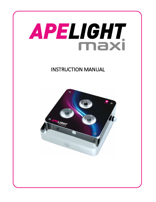
Table of ContentsSafety Instructions (1)Warning (2)General (3)Operation (4)Turn On and Off (4)Assignment of a Group (5)Using the Remote Control (5)List of Programs (7)Battery State/Charging (8)Disabling of the Battery Status Indicator (9)Enabling of the Battery Status Indicator (9)W-Ape Transceiver (10)Group (10)Control Mode (10)More Functions and Updates (12)Pairing (12)Pairing an ApeRemote with a Fixture: (12)Reset or Update of Firmware (13)Troubleshooting (14)Disposal (16)DMX Modes/DMX Sheets (17)3 Channel Mode (17)4 Channel Mode (18)8 Channel Mode (19)Safety Instructions›The ApeLight Maxi generates heat during operation and while charging. Therefore, make sure there is adequate ventilation and do not cover the light.›If you charge the ApeLight Maxi in the Tourcase (optional), the ApeLight Maxi Tourcase must remainopen.›Do not use the ApeLight Maxi in areas where the use of radio equipment is prohibited.›Do not look directly into the LEDs. This can cause damage to the eyes.Warning›All ApeLabs products use the same charging/power cord.Ape Labs products are specifically designed andengineered based on the Ape Labs power source (ApeLabs PSU). Do not use a different charging/power cord to power or charge the units (other than the Ape Labscharging road cases or Ape Labs PSU). Using a different power source may void your warranty.General›The ApeLight Maxi has three power LEDs below the lenses.›This device has 20 built-in auto programs. (See “List of Programs” below for details). Scroll thru the differentpre-sets with the left and right buttons on theApeRemote. If you’re on a static color, the Speed Up/Slow Down buttons will control the strobe speed. Ifyou’re on a chase program, they will control the colorchanging speed. By default, the Speed is set to it’slowest setting, which stops the speed effect.›This device can be wirelessly controlled with either the ApeRemote or W-Ape Transceiver (in combination with your favorite DMX controller).›All Ape Labs fixtures can be mixed/matched and controlled in the same room with the same remote (or DMX controller). To control certain fixtures differentlyfrom others in the same room, address the fixtures at the time they are turned on. For use with the ApeRemote,each fixture can be assigned to one of four groups. (See “Operation” section below for details on setting thefixture group).›If more than four groups are needed in a room, additional remotes can be used to add four additionalgroups per remote, as long as the added remotes arepaired with the respective light fixtures. (“See PairingSection” for additional details)›For use with the W-Ape (and a DMX controller), each fixture can be assigned to a DMX-512 address. Bydefault, the device is set to DMX address one, but it can be assigned to any address when it is turned on by going into Set-Up mode on the W-Ape.›The device has a built-in microphone. It can be activated on the remote control to create sound active effects. OperationTurn On and Off›Press the button on the back of the ApeLight Maxi for about one second. The unit turns on and remembers the previously selected program/brightness.›To turn the device off, press the button again for about a second.Note: The ApeLight Maxi ignores very short presses of the power button to prevent unintentional operation.Assignment of a GroupEach Ape Labs lighting fixture can be assigned to a specific group (so certain fixtures can be controlled differently than others in the same room).›Immediately after turning the ApeLight Maxi on, the current group setting of the ApeLight Maxi flashes on the remote control. (Factory setting is group 1.)›While the group LED is flashing, tap the Group Button again to change groups. The selected group LED willchange as you tap the Group Button.Note: The remote control switches to a power-save mode after a few minutes and will not detect the power-on event of a ApeLight Maxi. Press any key of remote control to stop the power-save mode.Using the Remote Control›To select the group you’d like to control, tap the “Group”button until the group LED is lit up. To control all groups at once, press and hold the “Group” button until all four group LEDs light up.›Programs, brightness, speed and sound active mode can be controlled by the corresponding keys (see figure).List of ProgramsNo Program1 White2 Red3 Orange4 Amber5 Lime6 Green7 Green/Blue8 Blue/Green9 Blue10 Blue/Magenta11 Magenta12 Red/White13 Green/White14 Blue/White15 Red > Blue16 Magenta > White17 White > Blue18 Red/White > Green/White > Blue/White19 Amber > Magenta > Blue20 Rainbow (All Colors)Hint: A long press on the left arrow will provide a static white color. A long press on the right arrow will provide a rainbow program. A long press on “Slow Down” stops a flash effect/color change in a multi-color program and will stay on single color. A long press on “Speed Up” will toggle between colors in selected program. In a multi-color program, the “Slow Down” button will also provide a fade effect opposed to flash effect/color change. In the Rainbow Program, a flash effect/color change will not occur, only a fade effect or single random color. Battery State/Charging›If the brightness of the ApeLight Maxi is reduced to zero (by “Power” or ”Dimmer” button of the remote control), the fixture will show the battery state at low brightness: o LEDs glow green: battery level above 50%o LEDs glow red: battery level below 50%Note: The calculation of the battery level needs at least one full charge/discharge cycle.›If the battery is completely empty, the device will blink 3 times red and turn itself off. Connect the provided power supply (18V DC) or put the device into the Tourcase.›If the battery charge is dropped to extremely low, the fixture may not blink Red (or show any signs of charging) during the first two hours of charging.›The ApeLight Maxi flashes red while charging. As soon as the battery is fully charged, the device will flash green.›The device can also be used while a power supply is connected. The battery will charge very slowly. Disabling of the Battery Status IndicatorThe red/green glowing indicator of the battery level can be disabled.›Step 1: Press and hold the power button on fixture until it flashes blue/white (This is also placing the fixture into Service Mode).›Step 2: Remove the battery compartment out of the ApeRemote.›Step 3: Slide the battery compartment back into the remote while pushing the “flashlight” symbol. (Remote will be flashing red on groups 1 & 4).›Step 4: Push the “Dim” button on the remote.›Step 5: Press the power button on fixture one time. ›Step 6: Press the “Power” button on the remote. Enabling of the Battery Status Indicator›Step 1: Press and hold the power button on fixture until it flashes blue/white (This is also placing the fixture into Service Mode).›Step 2: Remove the battery compartment out of the ApeRemote.›Step 3: Slide the battery compartment back into the remote while pushing the “flashlight” symbol. (Remote will be flashing red on groups 1 & 4).›Step 4: Push the “Bright” button on the remote.›Step 5: Press the power button on fixture one time.›Step 6: Press the “Power” button on the remote.W-Ape TransceiverMultiple W-Apes can be used in the same room on different universes if they are set to different groups.W-Ape has the following built-in modes (selected withUp/Down buttons on left of unit). Pressing the +/- buttons on the right of the unit will scroll thru the different options of each mode. If a light fixture is in set-up mode with the W-Ape, the screen will display info for the light fixture rather than the W-Ape.Group›Use +/- buttons to select the specific group.Control Mode›Sound Master: While the W-Ape is set to Sound Master mode, it will use the internal mic built in to the W-Ape to sync the Sound Active feature among all light fixtures(instead of using the internal mic built in to each fixture).In this mode, units will be controlled with an ApeRemote, thru the W-Ape. This feature extends the wireless range on the remote from it’s rated 200ft range, to the W-Ape’s rated wireless range of 3,000ft.›DMX: To use DMX controller, set W-Ape to “DMX” and connect your DMX controller to W-Ape input with 3-pin DMX cable.›W-Ape (Receiver): If multiple W-Apes are being used in one room, some W-Ape’s can be set as a receiver. In this case, set W-Ape to “W-Ape (Reciever)” and connect a 3-pin DMX cable from the DMX output of the W-Ape to the DMX input of the light fixture (to wirelessly control afixture that does not have wireless DMX built-in, such asa fixture from a brand other than Ape Labs).Info›Battery: During set-up mode, this will display the precise battery level of each light fixture.›Serial: This will display the serial number of the fixture. ›Firmware: This will display the firmware version of the fixture.DMX Mode›During set-up mode with given fixture, this will let you select the number of DMX mode for the fixture.o Off: W-APE/DMX-Mode is not activated - the device is only controllable by the remote control o3C: 3 channels: Dimmer, Program, Speedo4C: 4 channels: Red, Green, Blue, White (each is 1-DMX channel/8 Bit)o8C: 8 channels: Red, Green, Blue, White (each is 2-DMX channels/16 Bit: coarse + fine)More Functions and UpdatesPairingApe Labs lights and ApeRemotes can be paired permanently to one another so that they will no longer synchronize with other fixtures. Pair as many lights to one remote as you would like. This will allow users to create up to four groups on one remote and up to four more groups on each additional remote that is being used at the same time. Pairing an ApeRemote with a Fixture:›Step 1: Remove battery from ApeRemote›Step 2: While holding down flashlight button, insert battery into ApeRemote (if done correctly, group 1 and group 4 will flash on remote).›Step 3: Turn on fixture with long press on power button(5 seconds – if done correctly, fixture will blink blue).›Step 4: Press Right Arrow button to pair remote and light.›Step 5: Turn light off then back on. It will now only be controlled with that specific remote.›Step 6: To unpair, follow steps 1-3, then press Left Arrow button to unpair.NOTE: In case you lose paired remote, any remote can be used to unpair fixtures.Reset or Update of FirmwarePress and hold the power button of the ApeLight Maxi for about 10 seconds. The device will restart and stay in update mode for about 15 seconds (flashes red). During this period, an update can be started. If no update occurs, the device will go back to normal function. You can find firmware updates at or at your dealer.TroubleshootingProblem PossibleReason SolutionApeLight Maxi is dimmed and flashes sometimes Soundactivemode isactive.Press the microphonebutton on the remotecontrol to deactivatesound active mode.ApeLight Maxi flashes slowly Regularflash effectLong press (2s) “SlowDown” on the remotecontrol, to reduce theeffect speed to 0.ApeLight Maxi flashes 3 times red and turns itself off BatteryemptyConnect the powersupply to charge thebattery.Problem PossibleReason SolutionApeLight Maxi cannot be turned on Powerbutton waspressed tooshortPress and hold the buttonfor about 1 secondBrightness isat lowestlevel.Press “Brighter” button onthe remote controlBattery isdeeplydischargedConnect the 18V powersupply or charge theApeLight Maxi in theTourcase. It may takeseveral hours until thecharge will startApeLight Maxi glows permanently red/green RegularbatterystatusindicatorThe battery status will beshown by a glow of LEDs.This feature can bedisabled. Instructions canbe found above in“Disabling of the BatteryStatus Indicator” sectionDisposalIf the ApeLight Maxi is to be put out ofoperation, take it to a local recycling facility for a disposal which is not harmful to the environment. Never throw used batteries or defective rechargeable batteries into the household disposal: Always take them to a special waste disposal (e. g. collecting container at your retailer).DMX Modes/DMX Sheets3 Channel Mode: Dimmer, Program, SpeedThis mode can be used with other Ape Labs products, i.e. LightCan, MobiLight4, ApeStick4, ApeLight ART, and ApeLight Mini.Ch DMX Function1 0 - 255 Dimmer 0 - 100%2 0 - 5 Prog 1 White with fadesteps of 6*Prog 2 - 19 ... with fade114 - 127 Prog 20 Rainbow with fade128 - 133 Prog 1 White without fadesteps of 6*Prog 2 - 19 ... without fade242 - 255 Prog 20 Rainbow without fade3 0 - 255 Prog Speed 0 - 100%* Channel 1: Program 1-20 without fade and 1-20 with fade start at DMX value 0, 6, 12, 18, 24, 30, 36, 42, 48, 54, 60, 66, 72, 78, 84, 90, 96, 102, 108, 114, 128, 134, 140, 146, 152, 158, 164, 170, 176, 182, 188, 194, 200, 206, 212, 218, 224, 230, 236, 242Mode)This is the default DMX mode.This mode can be used with other Ape Labs products, i.e. LightCan, ApeStick4, and ApeLight Mini.If your DMX controller has no matching profile, use a “Generic/RGBW LED 8 Bit”.Channel DMX Function1 0 - 255 red 0 - 100%2 0 - 255 green 0 - 100%3 0 - 255 blue 0 - 100%4 0 - 255 white 0 - 100%This mode can be used with other Ape Labs products, i.e. LightCan, ApeStick4,and ApeLight Mini.If your DMX controller has no matching profile, use a “Generic/RGBW LED 16 Bit.”Channel DMX Function1 0 - 255 red 0 - 100%2 0 - 255 red fine3 0 - 255 green 0 - 100%4 0 - 255 green fine5 0 - 255 blue 0 - 100%6 0 - 255 blue fine7 0 - 255 white 0 - 100%8 0 - 255 white fine。
MAXIM MAX5012 说明书

现货库存、技术资料、百科信息、热点资讯,精彩尽在鼎好!_______________General DescriptionThe MAX5012 is a 12-bit, 100Msps digital-to-analog converter (DAC) designed for digital modulation, direct digital synthesis, high-resolution imaging, and arbitrary-waveform-generation applications. This device is pin-for-pin compatible with the AD9712 with significantly improved settling time and glitch-energy performance. The MAX5012 is an ECL-compatible device. It features a fast 13ns settling time and low 15pV-s glitch impulse energy, which results in excellent spurious-free dynamic range characteristics.The MAX5012 is available in a 28-pin plastic DIP or PLCC package in the -40°C to +85°C extended-industrial temperature range.________________________ApplicationsFast-Frequency-Hopping Spread-Spectrum RadiosDirect-Sequence Spread-Spectrum Radios Digital RF/IF ModulationMicrowave and Satellite Modems Test and Measurement Instrumentation____________________________Featureso 12-Bit, 100Msps DAC o ECL-Compatible Inputs o Low Power: 600mW o 1/2LSB DNLo 40MHz Multiplying Bandwidtho Extended-Industrial Temperature Range o Superior Performance over AD9712:Improved Settling Time: 13ns Improved Glitch Energy: 15pV-s Master/Slave LatchesMAX501212-Bit, 100Msps ECL DAC________________________________________________________________Maxim Integrated Products1_________________________________________________________Functional Diagram19-1271; Rev 0; 8/97Pin Configurations appear at end of data sheet.For the latest literature: , or phone 1-800-998-8800.For small orders, phone 408-737-7600 ext. 3468.M A X 501212-Bit, 100Msps ECL DAC 2_______________________________________________________________________________________ABSOLUTE MAXIMUM RATINGSELECTRICAL CHARACTERISTICS(V EE = -5.2V, R SET = 7.5k Ω, CONTROL AMP IN = REF OUT, V OUT = 0V, T A = T MIN - T MAX ,unless otherwise noted.)Stresses beyond those listed under “Absolute Maximum Ratings” may cause permanent damage to the device. These are stress ratings only, and functional operation of the device at these or any other conditions beyond those indicated in the operational sections of the specifications is not implied. Exposure to absolute maximum rating conditions for extended periods may affect device reliability.Supply VoltagesNegative Supply Voltage (V EE ).............................................-7V A/D Ground Voltage Differential..........................................0.5V Input VoltagesDigital Input Voltage (D1–D12, Latch Enable)............0V to V EE Control Amp Input Voltage Range...............................0V to -4V Reference Input Voltage Range (V REF )..................-3.7V to V EE Output CurrentsInternal-Reference Output Current.................................500µAControl-Amplifier Output Current..................................±2.5mA Continuous Power DissipationPlastic DIP (derate 14.29mW/°C above +70°C).............1.14W PLCC (derate 10.53mW/°C above +70°C)...................842mW Operating Temperature Range ...........................-40°C to +85°C Junction Temperature......................................................+150°C Lead Temperature (soldering, 10sec).............................+300°C Storage Temperature Range.................................-65 to +150°CMAX501212-Bit, 100Msps ECL DAC_______________________________________________________________________________________3Note 1:Gain is measured as a ratio of the full-scale current to I SET . The ratio is nominally 128.Note 2:Measured as voltage at mid-scale transition to ±0.024%; R L = 50Ω.Note 3:Measured from the rising edge of Latch Enable to where the output signal has left a 1LSB error band.Note 4:Glitch is measured as the largest single transient.Note 5:ELECTRICAL CHARACTERISTICS (continued)(V EE = -5.2V, R SET = 7.5k Ω, CONTROL AMP IN = REF OUT, V OUT = 0V, T A = T MIN - T MAX , unless otherwise noted.)TEST LEVEL CODESTEST LEVELTEST PROCEDUREAll electrical characteristics are subject to the followingconditions:All parameters having min/max specifications are guar-anteed. The Test Level column indicates the specific device testing actually performed during production and Quality Assurance inspection. Any black section in the data column indicates that the specification is not tested at the specified condition.I IIIII IV V VI100% production tested at the specified temperature.100% production tested at T A = +25°C, and sample tested at the specified temperatures.QA sample tested only at the specified temperatures.Parameter is guaranteed (but not tested) by design and characterization data.Parameter is a typical value for information purposes only.100% production tested at T A = +25°C. Parameter is guaranteed over specified temperature range.M A X 501212-Bit, 100Msps ECL DAC 4_______________________________________________________________________________________NAME FUNCTION1–10D2–D11Digital Input Bits 2–11PIN 13Analog ReturnAnalog Return Ground 12, 21Digital V EE Digital Negative Supply (-5.2V)11D12 (LSB)Digital Input Bit 12 (LSB)______________________________________________________________Pin Description14I OUT Analog Current Output 15, 25Analog V EEAnalog Negative Supply (-5.2V)16I _OUTComplementary Analog Current Output 17Ref In Voltage Reference Input20Ref Out Internal Voltage Reference Output. Ref Out is normally connected to Control Amp In.19Control Amp InInternal Control Amplifier Input. Control Amp In is normally connected to Ref Out (if not con-nected to external reference).18Control Amp Out Internal Control Amplifier Output. Control Amp Out is normally connected to Ref In.26Latch Enable Latch Control Line 24R SET *Connection for External Resistance Reference. R SET is used with the internal amplifier (nominally 7.5k Ω).23N.C.No Connection. Not internally connected.22Ref GND Ground Return for Internal Voltage Reference and Amplifier 28D1 (MSB)Digital Input Bit 1 (MSB)27DGND Digital Ground Return *Full-Scale Current Out = 128 (Control Amp In/R SET )Figure 1. Timing Diagram12-Bit, 100Msps ECL DACMAX5012MAX5012Figure 2. Typical Interface Circuit_______________________________________________________________________________________5M A X 501212-Bit, 100Msps ECL DAC 6_________________________________________________________________________________________________________________________________________________Pin ConfigurationsMAX501212-Bit, 100Msps ECL DAC_______________________________________________________________________________________7________________________________________________________Package InformationM A X 501212-Bit, 100Msps ECL DAC ___________________________________________Package Information (continued)Maxim cannot assume responsibility for use of any circuitry other than circuitry entirely embodied in a Maxim product. No circuit patent licenses are implied. Maxim reserves the right to change the circuitry and specifications without notice at any time.8_____________________Maxim Integrated Products, 120 San Gabriel Drive, Sunnyvale, CA 94086 408-737-7600©1997 Maxim Integrated ProductsPrinted USAis a registered trademark of Maxim Integrated Products.。
MAX512使用手册

MAX 512 MOVING LIGHT CONTROLLER电脑灯控制台 - 用户手册(软件版本VER:3.8)Net.DO力度灯控设备有限公司NETDO LIGHTING CONTROL EQUIPMENT CO.,LTD目录一、综述 (4)1.1 功能特点 (4)1.2 规格参数 (4)二、安装 (5)2.1安全使用注意事项 (5)2.2 连接供电电源 (5)2.3 连接电脑灯和数码调光设备 (5)2.4 音频信号源 (5)三、操作使用 (6)3.1 面板图 (6)3.2 常用词汇介绍 (7)3.3 键盘部分 (7)3.4 推杆、数据轮部分 (9)3.5 后板接口说明 (10)四、设置电脑灯 (11)4.1了解您的电脑灯 (11)4.2 X/Y(PAN/TILT)通道解析 (11)4.3电脑灯的DMX512 地址码分配及X/Y设置 (11)4.3.1 固定分配电脑灯地址: (11)4.3.2动态分配电脑灯地址: (11)4.3.3设置的方法及步骤: (12)五、电脑灯的手动运行(手动场景) (13)5.1 CHANNEL通道推杆与数据轮 (13)5.2 电脑灯的手动运行 (13)5.3 取消电脑灯的手动运行 (13)六、场景编辑 (14)6.1 重要提示 (14)6.2 场景的编辑记录步骤 (14)6.3 场景的复制 (14)七、走灯程序编辑 (15)7.1 走灯程序的编辑步骤: (15)八、运行 (17)8.1 运行场景 (17)8.2 运行走灯程序 (17)8.2.1 查看各走灯程序的运行状态 (18)8.2.2 走灯的同步触发模式 (18)8.2.3 调节自动模式(Auto)下的SPEED% 及CROSS% 值 (18)九、图形轨迹(SHAPE) (19)9.1 图形轨迹发生器 (19)9.2 图形的调用与编辑 (19)9.3 图形的停止与运行 (21)9.4 清除电脑灯的图形调用 (21)9.5 查看图形的调用情况 (21)9.6 图形的使用技巧 (21)十、数据文件的加载与保存 (24)10.1 闪存卡的使用 (24)10.2 文件的保存(SA VE) (24)10.3 文件的加载(LOAD) (24)十一.数据的初始化 (25)十二.附表 (25)12.1 LCD显示内容解释: (25)1.1 功能特点MAX512电脑灯光控制台可同时控制30台最大32通道的电脑灯,其核心微电脑采用新的技术,使其获得了更强、更人性化的功能。
MAX5100AEUP-T资料

For free samples & the latest literature: , or phone 1-800-998-8800.For small orders, phone 1-800-835-8769.General DescriptionThe MAX5100 parallel-input, voltage-output, quad 8-bit digital-to-analog converter (DAC) operates from a sin-gle +2.7V to +5.5V supply and comes in a space-sav-ing 20-pin TSSOP package. I nternal precision buffers swing Rail-to-Rail ®, and the reference input range includes both ground and the positive rail. All four DACs share a common reference input.The MAX5100 provides double-buffered logic inputs:four 8-bit buffer registers followed by four 8-bit DAC registers. This keeps the DAC outputs from changing during the write operation. An asynchronous control pin, LDAC , allows for simultaneous updating of the DAC registers.The MAX5100 features a shutdown mode that reduces current to 1nA, as well as a power-on reset mode that resets all registers to code 00 hex on power-up.ApplicationsDigital Gain and Offset Adjustments Programmable Attenuators Portable Instruments Power-Amp Bias ControlFeatureso +2.7V to +5.5V Single-Supply Operationo Ultra-Low Supply Current0.4mA while Operating 1nA in Shutdown Modeo Ultra-Small 20-Pin TSSOP Package o Ground to V DD Reference Input Range o Output Buffer Amplifiers Swing Rail-to-Rail o Double-Buffered Registers for Synchronous Updating o Power-On Reset Sets All Registers to ZeroMAX5100+2.7V to +5.5V , Low-Power, Quad, Parallel 8-Bit DAC with Rail-to-Rail Voltage Outputs________________________________________________________________Maxim Integrated Products119-1557; Rev 0; 10/99Pin ConfigurationOrdering InformationRail-to-Rail is a registered trademark of Nippon Motorola, Ltd.M A X 5100+2.7V to +5.5V , Low-Power, Quad, Parallel 8-Bit DAC with Rail-to-Rail Voltage Outputs 2_______________________________________________________________________________________ABSOLUTE MAXIMUM RATINGSELECTRICAL CHARACTERISTICS(V DD = V REF = +2.7V to +5.5V, R L = 10k Ω, C L = 100pF, T A = T MIN to T MAX , unless otherwise noted. Typical values are at V DD = V REF = +3V and T A = +25°C.)Stresses beyond those listed under “Absolute Maximum Ratings” may cause permanent damage to the device. These are stress ratings only, and functional operation of the device at these or any other conditions beyond those indicated in the operational sections of the specifications is not implied. Exposure to absolute maximum rating conditions for extended periods may affect device reliability.V DD to GND..............................................................-0.3V to +6V D_, A_, WR , SHDN, LDAC to GND...........................-0.3V to +6V REF to GND................................................-0.3V to (V DD + 0.3V)OUT_ to GND...........................................................-0.3V to V DD Maximum Current into Any Pin.........................................±50mA Continuous Power Dissipation (T A = +70°C)20-Pin TSSOP (derate 7.0mW/°C above +70°C).......559mWOperating Temperature RangeMAX5100_EUP ..............................................-40°C to +85°C Maximum Junction Temperature.....................................+150°C Storage Temperature Range.............................-65°C to +150°C Lead Temperature (soldering, 10sec).............................+300°CMAX5100+2.7V to +5.5V , Low-Power, Quad, Parallel 8-Bit DAC with Rail-to-Rail Voltage Outputs_______________________________________________________________________________________3Note 1:Reduced digital code range (code 00 hex to code F0 hex) due to swing limitations when the output amplifier is loaded.Note 2:Gain error is: [100 (V F0,meas - ZCE - V F0,ideal ) / V REF ]. Where V F0,meas is the DAC output voltage with input code F0 hex,and V F0,ideal is the ideal DAC output voltage with input code F0 hex (i.e., V REF ·240 / 256).Note 3:Output settling time is measured from the 50% point of the falling edge of WR to ±1/2LSB of V OUT ’s final value.Note 4:Channel-to-channel isolation is defined as the glitch energy at a DAC output in response to a full-scale step change on anyother DAC output. The measured channel has a fixed code of 80 hex.Note 5:Digital feedthrough is defined as the glitch energy at any DAC output in response to a full-scale step change on all eightdata inputs with WR at V DD .Note 6:R L = ∞, digital inputs at GND or V DD .Note 7:Timing measurement reference level is (V IH + V IL ) / 2.Note 8:If LDAC is activated prior to WR ’s rising edge, it must stay low for t LD (or longer) after WR goes high.ELECTRICAL CHARACTERISTICS (continued)(V DD = V REF = +2.7V to +5.5V, R L = 10k Ω, C L = 100pF, T A = T MIN to T MAX , unless otherwise noted. Typical values are at V DD = V REF = +3V and T A = +25°C.)M A X 5100+2.7V to +5.5V , Low-Power, Quad, Parallel 8-Bit DAC with Rail-to-Rail Voltage Outputs 4_______________________________________________________________________________________Typical Operating Characteristics(V DD = V REF = +3V, R L = 10k Ω, C L = 100pF, code = FF hex, T A = +25°C, unless otherwise noted.)00.40.20.80.61.01.20426810DAC ZERO-CODE OUTPUT VOLTAGEvs. SINK CURRENTSINK CURRENT (mA)V O U T (V )2143560426810DAC FULL-SCALE OUTPUT VOLTAGEvs. SOURCE CURRENTSOURCE CURRENT (mA)V O U T (V )180220200260240320300280340-400-2020406080100SUPPLY CURRENT vs. TEMPERATURETEMPERATURE (°C)S U P P L Y C U R R E N T (µA )14018016022020028026024030001.00.5 1.52.0 2.53.0SUPPLY CURRENT vs. REFERENCE VOLTAGE(V DD = 3V)REFERENCE VOLTAGE (V)S U P P L Y C U R R E N T (µA )20024022030028026032001.00.5 1.52.0 2.53.0 3.54.0 4.55.0SUPPLY CURRENT vs. REFERENCE VOLTAGE(V DD = 5V)REFERENCE VOLTAGE (V)S U P P L Y C U R R E N T (µA )-80-60-70-50-20-10-30-40000.51.01.52.02.5TOTAL HARMONIC DISTORTION PLUS NOISE AT DAC OUTPUT vs. REFERENCE AMPLITUDEREFERENCE AMPLITUDE (V p-p )T H D + N O I S E (d B )MAX5100+2.7V to +5.5V , Low-Power, Quad, Parallel 8-Bit DAC with Rail-to-Rail Voltage Outputs_______________________________________________________________________________________5-80-60-70-50-20-10-30-400110100TOTAL HARMONIC DISTORTION PLUS NOISE AT DAC OUTPUT vs. REFERENCE FREQUENCYFREQUENCY (kHz)T H D + N O I S E (d B )0-900.011010.1REFERENCE INPUT FREQUENCY RESPONSE-60-80-20-4010-50-70-10-30FREQUENCY (MHz)O U T P U T A M P L I T U D E (d B )21WORST-CASE 1LSB DIGITAL STEP CHANGE(NEGATIVE)1µs/divCH1 = LDAC, 2V/div CH2 = V OUTA , 50mV/div,AC-COUPLED DAC CODE FROM 80 TO 7F HEX21WORST-CASE 1LSB DIGITAL STEP CHANGE(POSITIVE)1µs/div CH1 = LDAC, 2V/div CH2 = V OUTA , 50mV/div,AC-COUPLED DAC CODE FROM 7F TO 80 HEX21DIGITAL FEEDTHROUGH GLITCH IMPULSE(0 TO 1 DIGITAL TRANSITION)20ns/div CH1 = D7, 2V/divCH2 = V OUTA , 2mV/div,AC-COUPLED0 TO 1 DIGITAL TRANSITION ON ALL DATA BITS (WITH WR HIGH, LDAC LOW)21DIGITAL FEEDTHROUGH GLITCH IMPULSE(1 TO 0 DIGITAL TRANSITION)20ns/divCH1 = D7, 2V/divCH2 = V OUTA , 2mV/div,AC-COUPLED1 TO 0 DIGITAL TRANSITION ON ALL DATA BITS (WITH WR HIGH, LDAC LOW)21POSITIVE SETTLING TIME1µs/div CH1 = WR, 2V/div CH2 = V OUTA , 2V/div DAC CODE FROM 10 TO F0 HEX21NEGATIVE SETTLING TIME1µs/div CH1 = WR, 2V/div CH2 = V OUTA , 2V/div DAC CODE FROM 10 TO F0 HEX0.50.40.30.20.10-0.1-0.2-0.3-0.4-0.50326496128160192224256INTEGRAL AND DIFFERENTIAL NONLINEARITYvs. DIGITAL CODEDIGITAL CODEI N L /D N L (L S B )R L = ∞DNLINLTypical Operating Characteristics (continued)(V DD = V REF = +3V, R L = 10k Ω, C L = 100pF, code = FF hex, T A = +25°C, unless otherwise noted.)M A X 5100+2.7V to +5.5V , Low-Power, Quad, Parallel 8-Bit DAC with Rail-to-Rail Voltage Outputs 6_______________________________________________________________________________________Pin DescriptionDAC Address Select Bit (MSB)A116Shutdown. Connect SHDN to GND for normal operation.SHDN 5Write Input (active low). Use WR to load data into the DAC input latch selected by A0 and A1.WR 6Data Inputs 7–0D7–D07–14Load DAC Input (active low). Drive the asynchronous LDAC input low to transfer the contents of all input latches to their respective DAC latch.LDAC 15Reference Voltage InputREF 4Positive Supply Voltage. Bypass V DD to GND using a 0.1µF capacitor.V DD 3PIN DAC A Voltage OutputOUTA 2DAC B Voltage Output OUTB 1FUNCTIONNAME Detailed DescriptionDigital-to-Analog SectionThe MAX5100 uses a matrix decoding architecture for the DACs. The external reference voltage is divided down by a resistor string placed in a matrix fashion.Row and column decoders select the appropriate tab from the resistor string to provide the needed analog voltages. The resistor network converts the 8-bit digital input into an equivalent analog output voltage in pro-portion to the applied reference voltage input. The resistor string presents a code-independent input impedance to the reference and guarantees a monoton-ic output.The device can be used in multiplying applications.The voltages are buffered by rail-to-rail op amps con-nected in a follower configuration to provide a rail-to-rail output. The functional block diagram for the MAX5100is shown in Figure 2.Low-Power Shutdown ModeThe MAX5100 features a shutdown mode that reduces current consumption to 1nA. A high voltage on the shutdown pin shuts down the DACs and the output amplifiers. I n shutdown mode, the output amplifiers enter a high-impedance state. When bringing thedevice out of shutdown, allow 13µs for the output to stabilize.Output Buffer AmplifiersThe DAC outputs are internally buffered by precision amplifiers with a typical slew rate of 0.6V/µs. The typical settling time to ±1/2LSB at the output is 6µs when loaded with 10k Ωin parallel with 100pF.Reference InputThe MAX5100 provides a code-independent input impedance on the REF input. The input impedance is typically 460k Ωin parallel with 15pF, and the reference input voltage range is 0 to V DD . The reference input accepts positive DC signals as well as AC signals with peak values between 0 and V DD . The voltage at REF sets the full-scale output voltage for the DAC. The out-put voltage (V OUT ) for any DAC is represented by a digitally programmable voltage source as follows:V OUT = (N B ·V REF ) / 256where N B is the numeric value of the DAC binary input code.Digital Inputs and Interface LogicI n the MAX5100, address lines A0 and A1 select the DAC that receives data from D0–D7, as shown in Table 1.DAC C Voltage OutputOUTC20DAC Address Select Bit (LSB)A017GroundGND 18DAC D Voltage Output OUTD 19When WR is low, the addressed DAC’s input latch is transparent. Data is latched when WR is high.The MAX5100 LDAC feature allows simultaneous updating of all four DACs. LDAC low latches the data in the data registers to the DAC registers. If simultaneous updating is not required, tie LDAC low to keep the DAC latches transparent. If WR and LDAC are low simultane-ously, avoid output glitches by ensuring that data is valid before the two signals go low. When the device powers up (i.e., V DD ramps up), all latches are internal-ly preset with code 00 hex.Applications InformationExternal ReferenceThe reference source resistance must be considerably less than the reference input resistance. To keep within 1LSB error in an 8-bit system, R S must be less than R REF / 256. Hence, maintain a value of R S <1k Ωto ensure 8-bit accuracy. If V REF is DC only, bypass REF to GND with a 0.1µF capacitor. Values greater than this improve noise rejection.Power SequencingThe voltage applied to REF should not exceed V DD at any time. I f proper power sequencing is not possible,connect an external Schottky diode between REF and V DD to ensure compliance with the absolute maximum ratings.Power-Supply Bypassing andGround ManagementDigital or AC transient signals on GND can create noise at the analog output. Return GND to the highest-quality ground available. Bypass V DD with a 0.1µF capacitor,located as close to V DD and GND as possible.Careful PC board ground layout minimizes crosstalk between the DAC outputs and digital inputs.Chip InformationTRANSISTOR COUNT: 6848MAX5100+2.7V to +5.5V , Low-Power, Quad, Parallel 8-Bit DAC with Rail-to-Rail Voltage Outputs_______________________________________________________________________________________7H = High state, L = Low state, X = Don’t careM A X 5100+2.7V to +5.5V , Low-Power, Quad, Parallel 8-Bit DAC with Rail-to-Rail Voltage Outputs Maxim cannot assume responsibility f or use of any circuitry other than circuitry entirely embodied in a Maxim product. No circuit patent licenses are implied. Maxim reserves the right to change the circuitry and specifications without notice at any time.8_____________________Maxim Integrated Products, 120 San Gabriel Drive, Sunnyvale, CA 94086 408-737-7600©1999 Maxim Integrated ProductsPrinted USAis a registered trademark of Maxim Integrated Products.Package Information。
华为_MA5100(MA5103) 操作手册_03-维护管理01-23 OAM管理
Line BIP error events of optical port Path BIP error events of optical port
: 4998168 : 2488
Section BIP error events of Optical port : 1666025
Corrected HEC error events of optical port : 0
描述 介绍 MA5100 的 OAM 管理. 介绍物理层 OAM 的配置操作。 介绍 ATM 层 OAM 的配置操作。
文档版本 04 (2006-10-25)
华为技术有限公司
23-1
23 OAM 管理
SmartAX MA5100/MA5103 操作手册
23.1 概述
业务描述 业务规格
ATM 网络包含复杂的拓扑结构和业务类型.OAM(Operation, Administration and Maintenance)提供了一种不中断业务的故障检测,故障定位,性能检测和连续性校验的功 能,通过对物理层误码的统计与 ATM 层信元的操作,提取网络及其节点的一些特定信 息,进行网络故障的检测与隔离,实时地监测连接的 QoS 性能。
举例
打开信元捕捉功能。
MA5100#oam configuration
23-4
华为技术有限公司
文档版本பைடு நூலகம்04 (2006-10-25)
SmartAX MA5100/MA5103 操作手册
〈frame Id/slotId〉[(0)/(0—15)]: 0/7 {pvc,pvp, cell-capture}: cell-capture {crc—error-cell}: crc-error—cell 〈switch>{on。, off}: on [unsupproted—cell]: unsupported-cell 〈switch> { on, off} : on [undefined—cell]:undefined—cell 〈switch〉 { on, off} : on set successfully。
MAX5251AEAP中文资料

For pricing delivery, and ordering information please contact Maxim/Dallas Direct!at 1-888-629-4642, or visit Maxim’s website at .__________________General DescriptionThe +3V MAX5251 combines four low-power, voltage-output, 10-bit digital-to-analog converters (DACs) and four precision output amplifiers in a space-saving, 20-pin package. I n addition to the four voltage outputs,each amplifier’s negative input is also available to the user. This facilitates specific gain configurations, remote sensing, and high output drive capacity, making the MAX5251 ideal for industrial-process-control applica-tions. Other features include software shutdown, hard-ware shutdown lockout, an active-low reset that clears all registers and DACs to zero, a user-programmable logic output, and a serial-data output.Each DAC has a double-buffered input organized as an input register followed by a DAC register. A 16-bit serial word loads data into each input/DAC register. The 3-wire serial interface is compatible with SPI ™/QSPI ™and MI CROWI RE™. I t allows the input and DAC regis-ters to be updated independently or simultaneously with a single software command. All logic inputs are TTL/CMOS-logic compatible.________________________ApplicationsDigital Offset and Gain Adjustment Microprocessor-Controlled Systems Industrial Process Controls Automatic Test Equipment Remote Industrial Controls Motion Control______________________________Featureso Four 10-Bit DACs with Configurable Output Amplifierso +3.0V to +3.6V Single-Supply Operationo Low Supply Current: 0.8mA Normal Operation3µA Shutdown Modeo Available in 20-Pin SSOPo Power-On Reset Clears all Registers and DACs to Zeroo SPI/QSPI and MICROWIRE Compatibleo Simultaneous or Independent Control of DACs Through 3-Wire Serial Interface o User-Programmable Digital Output o Schmitt-Trigger Digital Inputs for Direct Optocoupler Interfaceo 12-Bit Upgrade Available: MAX5253MAX5251+3V , Quad, 10-Bit Voltage-Output DACwith Serial Interface________________________________________________________________Maxim Integrated Products119-1172; Rev 1; 10/02SPI and QSPI are trademarks of Motorola, Inc. MICROWIRE is a trademark of National Semiconductor Corp.M A X 5251+3V , Quad, 10-Bit Voltage-Output DAC with Serial Interface 2_______________________________________________________________________________________ABSOLUTE MAXIMUM RATINGSELECTRICAL CHARACTERISTICS(V DD = +3.0V to +3.6V, AGND = DGND = 0V, REFAB = REFCD = 1.25V, R L = 5k Ω, C L = 100pF, T A = T MIN to T MAX , unless otherwise noted. Typical values are at T A = +25°C. Output buffer connected in unity-gain configuration (Figure 9).)Stresses beyond those listed under “Absolute Maximum Ratings” may cause permanent damage to the device. These are stress ratings only, and functional operation of the device at these or any other conditions beyond those indicated in the operational sections of the specifications is not implied. Exposure to absolute maximum rating conditions for extended periods may affect device reliability.V DD to AGND............................................................-0.3V to +6V V DD to DGND...........................................................-0.3V to +6V AGND to DGND..................................................................±0.3V REFAB, REFCD to AGND...........................-0.3V to (V DD + 0.3V)OUT_, FB_ to AGND...................................-0.3V to (V DD + 0.3V)Digital Inputs to DGND.............................................-0.3V to +6V DOUT, UPO to DGND................................-0.3V to (V DD + 0.3V)Continuous Current into Any Pin.......................................±20mA Continuous Power Dissipation (T A = +70°C)Plastic DIP (derate 8.00mW/°C above +70°C).................640mW SSOP (derate 8.00mW/°C above +70°C)......................640mW CERDIP (derate 11.11mW/°C above +70°C).................889mWOperating Temperature RangesMAX5251_C_P......................................................0°C to +70°C MAX5251_E_P...................................................-40°C to +85°C MAX5251BMJP................................................-55°C to +125°C Storage Temperature Range.............................-65°C to +150°C Lead Temperature (soldering, 10s).................................+300°CMAX5251+3V , Quad, 10-Bit Voltage-Output DACwith Serial Interface_______________________________________________________________________________________3ELECTRICAL CHARACTERISTICS (continued)(V DD = +3.0V to +3.6V, AGND = DGND = 0V, REFAB = REFCD = 1.25V, R L = 5k Ω, C L = 100pF, T A = T MIN to T MAX , unless otherwise noted. Typical values are at T A = +25°C. Output buffer connected in unity-gain configuration (Figure 9).)Note 1:Guaranteed from code 5 to code 1023 in unity-gain configuration.Note 2:Accuracy is better than 1LSB for V OUT = 6mV to V DD - 80mV, guaranteed by PSR test at the endpoints.Note 3:Remains operational with supply voltage as low as +2.7V.Note 4:R L = ∞, digital inputs at DGND or V DD .-4-8-12-16-20500k 1.0M 1.5M2.0M 2.5M3.0MR E L A T I V E O U T P U T (d B )REFERENCE VOLTAGE INPUT FREQUENCY RESPONSEFREQUENCY (Hz)I N L (L S B )-1.250.51.0 1.52.0REFERENCE VOLTAGE (V)2.50.250-0.25-0.50-0.75-1.00INTEGRAL NONLINEARITYvs. REFERENCE VOLTAGE1000950900850800750700650600550500-55-40-20020406080120100S U P P L Y C U R R E N T (µA )SUPPLY CURRENT vs. TEMPERATURETEMPERATURE (°C)__________________________________________Typical Operating Characteristics(V DD = +3.3V, T A = +25°C, unless otherwise noted.)M A X 5251+3V , Quad, 10-Bit Voltage-Output DAC with Serial Interface 4_______________________________________________________________________________________ELECTRICAL CHARACTERISTICS (continued)(V DD = +3.0V to +3.6V, AGND = DGND = 0V, REFAB = REFCD = 1.25V, R L = 5k Ω, C L = 100pF, T A = T MIN to T MAX , unless otherwise noted. Typical values are at T A = +25°C. Output buffer connected in unity-gain configuration (Figure 9).)MAX5251+3V , Quad, 10-Bit Voltage-Output DACwith Serial Interface_______________________________________________________________________________________52.7 2.83.02.9 3.1 3.2 3.3 3.4 3.6SUPPLY CURRENT vs. SUPPLY VOLTAGESUPPLY VOLTAGE (V)S U P P L Y C U R R E N T (µA )3.510009509008508007507006006505005500-2.50.010.1110100FULL-SCALE ERRORvs. LOADM A X 5251-03LOAD (k Ω)F U L L -S C A L E E R R O R (L S B )-1.0-1.5-2.0-0.5____________________________Typical Operating Characteristics (continued)(V DD = +3.3V, T A = +25°C, unless otherwise noted.)0.5000.1110100TOTAL HARMONIC DISTORTION PLUS NOISE vs. FREQUENCY0.050.100.150.200.250.30FREQUENCY (kHz)T H D + N O I S E (%)0.350.400.45-100OUTPUT FFT PLOT-60FREQUENCY (kHz)S I G N A L A M P L I T U D E (d B )-20-40-80-1000.51.22.6REFERENCE FEEDTHROUGHAT 1kHz-60FREQUENCY (kHz)S I G N A L A M P L I T U D E (d B )1.9 3.3 4.0-20-40-80REFAB INPUT SIGNALV REF = 1.6V P-P AT 1kHz R L = 5k ΩC L = 100pFOUTA FEEDTHROUGH10µs/div MAJOR-CARRY TRANSITIONMAX5251-07OUTB,AC-COUPLED 50mV/div5V/div2µs/divOUTA,AC-COUPLED 10mV/divDIGITAL FEEDTHROUGH (SCLK = 100kHz)MAX5251-08SCLK,2V/divCS = PDL = C L = 3.3V, DIN = 0VDAC A CODE SET TO 800 HEXDAC A CODE SWITCHING FROM 00C HEX TO FFC HEX DAC B CODE SET TO 800 HEX10µs/divGNDOUTB,AC-COUPLED 10mV/divANALOG CROSSTALKMAX5251-12OUTA,500mV/divSWITCHING FROM CODE 000 hex TO FB4 HEX OUTPUT AMPLIFIER GAIN = +2.610µs/divDYNAMIC RESPONSEMAX5251-13OUTA,500mV/divM A X 5251+3V , Quad, 10-Bit Voltage-Output DAC with Serial Interface 6___________________________________________________________________________________________________________________Typical Operating Characteristics (continued)(V DD = +3.3V, V REF = 1.25V, R L = 5k Ω, C L = 100pF, T A = +25°C, unless otherwise noted.)MAX5251+3V , Quad, 10-Bit Voltage-Output DACwith Serial Interface_______________________________________________________________________________________7______________________________________________________________Pin DescriptionSerial-Data Input DIN 9Serial-Clock Input SCLK 10Digital Ground DGND 11Serial-Data OutputDOUT 12User-Programmable Logic OutputUPO 13DAC B Output Amplifier FeedbackFBB 5Reference Voltage Input for DAC A and DAC BREFAB 6Clears All DACs and Registers. Resets all outputs (OUT_, UPO, DOUT) to 0, active low.CL 7Chip-Select Input. Active low.CS 8DAC B Output VoltageOUTB 4DAC A Output Voltage OUTA 3PIN DAC A Output Amplifier Feedback FBA 2Analog GroundAGND 1FUNCTIONNAME Power-Down Lockout. Active low. Locks out software shutdown if low.PDL 14Reference Voltage Input for DAC C and DAC D REFCD 15DAC C Output Amplifier Feedback FBC 16DAC C Output Voltage OUTC 17DAC D Output VoltageOUTD 18DAC D Output Amplifier Feedback FBD 19Positive Power SupplyV DD20M A X 5251+3V , Quad, 10-Bit Voltage-Output DAC with Serial Interface8______________________________________________________________________________________________________Detailed DescriptionThe MAX5251 contains four voltage-output digital-to-analog converters (DACs) that are easily addressed using a simple 3-wire serial interface. I t includes a 16-bit data-in/data-out shift register, and each DAC has a doubled-buffered input composed of an input register and a DAC register (see Functional Diagram ). In addi-tion to the four voltage outputs, each amplifier’s nega-tive input is available to the user.The DACs are inverted R-2R ladder networks that con-vert a digital input (10 data bits plus 2 sub-bits) into equivalent analog output voltages in proportion to the applied reference voltage inputs. DACs A and B share the REFAB reference input, while DACs C and D share the REFCD reference input. The two reference inputs allow different full-scale output voltage ranges for each pair of DACs. Figure 1 shows a simplified circuit dia-gram of one of the four DACs.Reference InputsThe two reference inputs accept positive DC and AC signals. The voltage at each reference input sets the full-scale output voltage for its two corresponding DACs. The reference input voltage range is 0V to (V DD - 1.4V). The output voltages (V OUT_)are repre-sented by a digitally programmable voltage source as:V OUT_= (V REF x NB / 1024 ) x Gainwhere NB is the numeric value of the DAC’s binary input code (0 to 1023), V REF is the reference voltage,and Gain is the externally set voltage gain.The impedance at each reference input is code depen-dent, ranging from a low value of 10k Ωwhen both DACs connected to the reference have an input code of 554 hex, to a high value exceeding several giga ohms (leakage current) with an input code of 000 hex.Because the input impedance at the reference pins is code dependent,load regulation of the reference source is important.The REFAB and REFCD reference inputs have a 10k Ωguaranteed minimum input impedance. When the two reference inputs are driven from the same source, the effective minimum impedance is 5k Ω. Driving the REFAB and REFCD pins separately improves reference accuracy.In shutdown mode, the MAX5251’s REFAB and REFCD inputs enter a high-impedance state with a typical input leakage current of 0.01µA.The reference input capacitance is also code depen-dent and typically ranges from 20pF with an input code of all 0s to 100pF at full scale.Output AmplifiersAll MAX5251 DAC outputs are internally buffered by pre-cision amplifiers with a typical slew rate of 0.6V/µs.Access to each output amplifier’s inverting input pro-vides the user greater flexibility in output gain setting/signal conditioning (see the Applications Information section).With a full-scale transition at the MAX5251 output, the typical settling time to ±1/2LSB is 12µs when loaded with 5k Ωin parallel with 100pF (loads less than 2k Ωdegrade performance).The MAX5251 output amplifier’s output dynamic responses and settling performances are shown in the Typical Operating Characteristics .Power-Down ModeThe MAX5251 features a software-programmable shut-down that reduces supply current to a typical value of 3µA. The power-down lockout pin (PDL ) must be high to enable shutdown mode. Writing 1100XXXXXXXXXXXX as the input-control word puts the MAX5251 in shutdown mode (Table 1).Figure 1. Simplified DAC Circuit DiagramMAX5251+3V , Quad, 10-Bit Voltage-Output DACwith Serial Interface_______________________________________________________________________________________9In shutdown mode, the MAX5251 output amplifiers and the reference inputs enter a high-impedance state. The serial interface remains active. Data in the input regis-ters is retained in shutdown, allowing the MAX5251 to recall the output states prior to entering shutdown. Exit shutdown mode either by recalling the previous config-uration or by updating the DACs with new data. When powering up the device or bringing it out of shutdown,allow 20µs for the outputs to stabilize.Serial-Interface ConfigurationsThe MAX5251’s 3-wire serial interface is compatible with both MI CROWI RE (Figure 2) and SPI /QSPI (Figure 3). The serial input word consists of two address bits and two control bits followed by 10+2 data bits (MSB first), as shown in Figure 4.The 4-bit address/control code determines the MAX5251’s response out-lined in Table 1. The connection between DOUT and the serial-interface port is not necessary, but may be used for data echo. Data held in the MAX5251’s shift register can be shifted out of DOUT and returned to the microprocessor (µP) for data verification.The MAX5251’s digital inputs are double buffered.Depending on the command issued through the serial interface, the input register(s) can be loaded without affecting the DAC register(s), the DAC register(s) can be loaded directly, or all four DAC registers can be updated simultaneously from the input registers (Table 1).Serial-Interface DescriptionThe MAX5251 requires 16 bits of serial data. Table 1lists the serial-interface programming commands. For certain commands, the 10+2 data bits are “don’t cares.” Data is sent MSB first and can be sent in two 8-bit packets or one 16-bit word (CS must remain low until 16 bits are transferred). The serial data is com-posed of two DAC address bits (A1, A0) and two con-trol bits (C1, C0), followed by the 10+2 data bits D9…D0, S1, S0 (Figure 4). Set both sub-bits (S0, S1) to zero. The 4-bit address/control code determines: •The register(s) to be updated•The clock edge on which data is to be clocked out through the serial-data output (DOUT)•The state of the user-programmable logic output (UPO)•I f the part is to go into shutdown mode (assuming PDL is high)•How the part is configured when exiting shutdown mode.Figure 2. Connections for MicrowireFigure 3. Connections for SPI/QSPIFigure 4. Serial-Data FormatM A X 5251Figure 5 shows the serial-interface timing requirements.The chip-select pin (CS ) must be low to enable the DAC’s serial interface. When CS is high, the interface control circuitry is disabled. CS must go low at least t CSS before the rising serial clock (SCLK) edge to prop-erly clock in the first bit. When CS is low, data is clocked into the internal shift register through the serial-data input pin (DIN) on SCLK’s rising edge. The maxi-mum guaranteed clock frequency is 10MHz. Data is latched into the appropriate MAX5251 input/DAC regis-ters on CS ’s rising edge.The programming command Load-All-DACs-From-Shift-Register allows all input and DAC registers to be simul-taneously loaded with the same digital code from the input shift register. The no operation (NOP) command leaves the register contents unaffected and is useful when the MAX5251 is configured in a daisy chain (see the Daisy Chaining Devices section). The command tochange the clock edge on which serial data is shifted out of DOUT also loads data from all input registers to their respective DAC registers.Serial-Data Output (DOUT)The serial-data output, DOUT, is the internal shift regis-ter’s output. The MAX5251 can be programmed so that data is clocked out of DOUT on SCLK’s rising edge (Mode 1) or falling edge (Mode 0). I n Mode 0, output data at DOUT lags input data at DI N by 16.5 clock cycles, maintaining compatibility with MI CROWI RE,SPI/QSPI, and other serial interfaces. In Mode 1, output data lags input data by 16 clock cycles. On power-up,DOUT defaults to Mode 0 timing.User-Programmable Logic Output (UPO)The user-programmable logic output, UPO, allows an external device to be controlled through the MAX5251serial interface (Table 1).+3V , Quad, 10-Bit Voltage-Output DAC with Serial Interface 10______________________________________________________________________________________Table 1. Serial-Interface Programming Commands“X” = Don’t care16-BIT SERIAL WORDFUNCTIONA1A0C1C0D9.................D0MSB.............LSB S1S0000110110101010110-bit DAC data 10-bit DAC data 10-bit DAC data 10-bit DAC data 00000000Load input register A; DAC registers unchanged.Load input register B; DAC registers unchanged.Load input register C; DAC registers unchanged.Load input register D; DAC registers unchanged.000110111111111110-bit DAC data 10-bit DAC data 10-bit DAC data 10-bit DAC data 00000000Load input register A; all DAC registers updated.Load input register B; all DAC registers updated.Load input register C; all DAC registers updated.Load input register D; all DAC registers updated.0100XXXXXXXXXX X X Update all DAC registers from their respective input registers (also exit shutdown mode).100010-bit DAC data 00Load all DAC registers from shift register (also exit shutdown mode).1100XXXXXXXXXX X X Enter shutdown mode (provided PDL = 1).0010XXXXXXXXXX X X UPO goes low (default).0110XXXXXXXXXX X X UPO goes high.0000XXXXXXXXXX X X No operation (NOP) to DAC registers1110XXXXXXXXXX X X Mode 1, DOUT clocked out on SCLK’s rising edge. All DAC registers updated.11XXXXXXXXXXXXMode 0, DOUT clocked out on SCLK’s falling edge. All DAC registers updated (default).MAX5251+3V , Quad, 10-Bit Voltage-Output DACwith Serial Interface______________________________________________________________________________________11Power-Down Lockout (PDL )The power-down lockout pin PDL disables software shutdown when low. When in shutdown, transitioning PDL from high to low wakes up the part with the output set to the state prior to shutdown. PDL could also be used to wake up the device asynchronously.Daisy Chaining DevicesAny number of MAX5251s can be daisy chained by connecting the DOUT pin of one device to the DIN pin of the following device in the chain (Figure 7).Since the MAX5251’s DOUT pin has an internal active pull-up, the DOUT sink/source capability determines the time required to discharge/charge a capacitive load. Refer to the serial-data-out V OH and V OL specifi-cations in the Electrical Characteristics.Figure 8 shows an alternate method of connecting sev-eral MAX5251s. I n this configuration, the data bus is common to all devices; data is not shifted through a daisy chain. More I/O lines are required in this configu-ration because a dedicated chip-select input (CS ) is required for each IC.Figure 5. Serial-Interface Timing DiagramFigure 6. Detailed Serial-Interface Timing DiagramM A X 5251+3V , Quad, 10-Bit Voltage-Output DAC with Serial Interface12______________________________________________________________________________________Figure 7. Daisy-Chaining MAX5251sFigure 8. Multiple MAX5251s Sharing a Common DIN LineMAX5251+3V , Quad, 10-Bit Voltage-Output DACwith Serial Interface______________________________________________________________________________________13__________Applications InformationUnipolar OutputFor a unipolar output, the output voltages and the refer-ence inputs have the same polarity. Figure 9 shows the MAX5251 unipolar output circuit, which is also the typi-cal operating circuit. Table 2 lists the unipolar output codes.For rail-to-rail outputs, see Figure 10. This circuit shows the MAX5251 with the output amplifiers configured with a closed-loop gain of +2.6 to provide 0V to 3.25V full-scale range when a 1.25V reference is used.Bipolar OutputThe MAX5251 outputs can be configured for bipolar operation using Figure 11’s circuit:V OUT = V REF [(2NB / 1024) - 1]where NB is the numeric value of the DAC’s binary input code. Table 3 shows digital codes (offset binary)and corresponding output voltages for Figure 11’s circuit.Table 2. Unipolar Code TableFigure 9. Unipolar Output Circuit( ) Sub-bitsM A X 5251Using an AC ReferenceIn applications where the reference has AC signal com-ponents, the MAX5251 has multiplying capability within the reference input range specifications. Figure 12shows a technique for applying a sine-wave signal to the reference input where the AC signal is offset before being applied to REFAB/REFCD. The reference voltage must never be more negative than DGND.The MAX5251’s total harmonic distortion plus noise (THD + N) is typically less than -72dB (full-scale code),given a 1V P-P signal swing and input frequencies up to 25kHz. The typical -3dB frequency is 650kHz, as shown in the Typical Operating Characteristics graphs.Digitally Programmable Current SourceThe circuit of Figure 13 places an NPN transistor (2N3904 or similar) within the op-amp feedback loop to implement a digitally programmable, unidirectional cur-rent source. This circuit can be used to drive 4–20mA current loops, which are commonly used in industrial-control applications. The output current is calculated with the following equation:I OUT = (V REF / R) x (NB / 1024)where NB is the numeric value of the DAC’s binary input code and R is the sense resistor shown in Figure 13.+3V , Quad, 10-Bit Voltage-Output DAC with Serial Interface 14______________________________________________________________________________________Figure 10. Unipolar Rail-to-Rail Output CircuitFigure 11. Bipolar Output Circuit Figure 12. AC Reference Input CircuitMAX5251+3V , Quad, 10-Bit Voltage-Output DACwith Serial Interface______________________________________________________________________________________15Power-Supply ConsiderationsOn power-up, all input and DAC registers are cleared (set to zero code) and DOUT is in Mode 0 (serial data is shifted out of DOUT on the clock’s falling edge).For rated MAX5251 performance, limit REFAB/REFCD to less than 1.4V below V DD . Bypass V DD with a 4.7µF capacitor in parallel with a 0.1µF capacitor to e short lead lengths and place the bypass capaci-tors as close to the supply pins as possible.Grounding and Layout ConsiderationsDigital or AC transient signals between AGND and DGND can create noise at the analog outputs. Tie AGND and DGND together at the DAC, then tie this point to the highest-quality ground available.Good printed circuit board ground layout minimizes crosstalk between DAC outputs, reference inputs, and digital inputs. Reduce crosstalk by keeping analog lines away from digital lines. Wire-wrapped boards are not recommended.Figure 13. Digitally Programmable Current Source__________________Pin ConfigurationM A X 5251+3V , Quad, 10-Bit Voltage-Output DAC with Serial Interface Maxim cannot assume responsibility for use of any circuitry other than circuitry entirely embodied in a Maxim product. No circuit patent licenses are implied. Maxim reserves the right to change the circuitry and specifications without notice at any time.16____________________Maxim Integrated Products, 120 San Gabriel Drive, Sunnyvale, CA 94086 408-737-7600©2002 Maxim Integrated ProductsPrinted USAis a registered trademark of Maxim Integrated Products._Ordering Information (continued)___________________Chip Information*Contact factory for availability and processing to MIL-STD-883.TRANSISTOR COUNT: 4337Package Information(The package drawing(s) in this data sheet may not reflect the most current specifications. For the latest package outline information go to /packages .)。
华为_MA5100(MA5103) 操作手册_03-维护管理01-21 补丁管理
Current patch number:3
Common patch number: 0
Temporary patch number: 0
Deactive patch number: 0
Active patch number: 0
Running patch number: 0
Begin to write FLASH......success
----结束
验证结果
使用show patch命令查询补丁信息。
huawei#showpatch
{<option>}{all,memory}:all
Patch version: V100R005B10D056
Patch area start address: 0x1540000
21.3
目的
加载后的补丁必须激活后才能运行。
考前须知
激活一个指定补丁号的补丁时,那么该补丁号及其前面的所有补丁都将被激活。如该版本有较多的补丁,那么只需激活最新的补丁即可。
去激活一个指定补丁号的补丁时,那么该补丁号及其后面的所有补丁都将去激活。
举例
激活加载的补丁。
huawei#patch activate
<patch number>{1-99}{all}:3
Are you sure to continue?(y/n) [y]:
Activating patch file......success
去激活补丁。
huawei#patch activate
<patch number>{1-99}{all}:3
21
关于本章
DMX512中文使用说明书
DMX512中文使用说明书一、四位数码管说明:XXXX*第一位代表CHASE,共有6个*第二位代表SCENSE,共有8个*第三四位代表BANK,共有30个*设置MIDI通道时第三四位代表MIDI通道,共有16个MIDI通道*一个CHASE最多可以包含240个SCENSE*一个BANK最多可以包含8个SCENSE*一个SCENSE最多可以包含192个通道(也可以说是12个SCANNER) SCANNER1:通道1~通道16SCANNER2:通道17~通道32以此类推SCANNER12:通道181~通道192*一个SCANNER最多可以包含16个通道*调节滑杆时显示数值或者百分比二、操作时请注意数码屏的指示灯在什么状态。
*BLANKOUT*STEP*PROGRAM*MUSIC TIGGER*AUTO TIGGER三、DMX512面板功能说明1、SCANNERS按下SCANNER键,其旁边的LED灯亮,其中连接8个通道的输出可被调节,在SCENS运行时,如果可调电位器控制为OFF,则调节电位器不会影响通道输出,但如果可调电位器控制为ON,则通道输出会随相应的可调电位器的改变而改变;2、SCENS按健按下一个SCENS键可触发SCENS或存入一个SCENS,第二个数码管头显示SCENS1-8;3、可调电位器调节可调电位器改变DMX的通道输出大小,最小是0最大为255或者从0%-100%,可调电位器1-8控制连续的八个通道;4、PAGE/SELECT键选择PAGE A或PAGE B,PAGE A为每个SCANNER的前八个通道PAGE B为每个SCANNER 的后八个通道;5、SPEED SLIDER推动这个推杆调整走灯速度;6、FADE TIME SLIDER推动这个推杆调整FADE TIME;7、LED DISPLAY8、BANK按键(↑/↓)第三位和第四位数码管显示BANKS(01-30),按下↑/↓键,BANK增大或减小,显示的SCENS 为该BANK里的SCENS;9、CHASE 1-CHASE 6键用于CHASES编程或CHASES运行的选择;10、PROGRAM键上电本机在走动运行状态,按下PROGRAM键盘2秒,编程指示灯闪动可编程SCENSR和CHASER,再按下PROGRAM键2秒,编程指示灯灭回到运行状态;11、MIDI/ADD键A、在运行状态按住MIDI键2秒,第3及第4位数码管闪动,通过↑或↓选择MIDI通道,再按MIDI键2秒结束MIDI通道的设置选择的MIDI通道被存贮;或者除↑/↓键以外的任何键都可结束MIDI通道的设置,不存贮所选取的MIDI通道;B、在编程状态,用于编辑;12、AUTO/DEL键A、在运行状态,按下AUTO/DEL键,自动触发指示灯亮,表示在自动触发状态,再按下AUTO 键退出自动触发状态,自动触发指示灯灭;B、在编程状态,用于SCENS及CHASE编程;13、MUSIC/BANK COPY键A、在运行状态,按下MUSIC键,声音触发指示灯亮,可由声音触发SCENS,再按一下MUSIC 键,声音触发指示灯灭,退出声音触发状态;B、在编程状态,用于SCENS及CHASE编程;14、TAPSYNC/DISPLAY键A:(1)、在AUTO运行状态,最后两次按下TAP SYNC/DISPLAY键决定SCENS运行的速率,最大时间为十分钟;(2)、不在AUTO运行状态,转换00-255或0%-100%;B:在编程状态(1)、对CHASE编程时,在步数显示和BANK显示之间转换;(2)、不在CHASE编程时转换00-255或0%-100%。
- 1、下载文档前请自行甄别文档内容的完整性,平台不提供额外的编辑、内容补充、找答案等附加服务。
- 2、"仅部分预览"的文档,不可在线预览部分如存在完整性等问题,可反馈申请退款(可完整预览的文档不适用该条件!)。
- 3、如文档侵犯您的权益,请联系客服反馈,我们会尽快为您处理(人工客服工作时间:9:00-18:30)。
For free samples & the latest literature: , or phone 1-800-998-8800.For small orders, phone 1-800-835-8769.General DescriptionThe MAX5102 parallel-input, voltage-output, dual 8-bit digital-to-analog converter (DAC) operates from a single +2.7V to +5.5V supply and comes in a space-saving 16-pin TSSOP package. I nternal precision buffers swing Rail-to-Rail ®, and the reference input range includes both ground and the positive rail. Both DACs share a common reference input.The MAX5102 has separate input latches for each of its DACs. Data is transferred to the input latches from a common 8-bit input port. The DACs are individually selected through address input A0 and are updated by bringing WR low.The MAX5102 features a shutdown mode that reduces current to 1nA, as well as a power-on reset mode that resets all registers to code 00 hex on power-up.ApplicationsDigital Gain and Offset Adjustment Programmable Attenuators Portable Instruments Power-Amp Bias ControlFeatureso +2.7V to +5.5V Single-Supply Operationo Ultra-Low Supply Current0.2mA while Operating 1nA in Shutdown Modeo Ultra-Small 16-Pin TSSOP Package o Ground to V DD Reference Input Range o Output Buffer Amplifiers Swing Rail-to-Rail o Power-On Reset Sets All Registers to ZeroMAX5102+2.7V to +5.5V , Low-Power, Dual, Parallel 8-Bit DAC with Rail-to-Rail Voltage Outputs________________________________________________________________Maxim Integrated Products119-1565; Rev 0; 10/99Pin ConfigurationOrdering InformationRail-to-Rail is a registered trademark of Nippon Motorola, Ltd.Functional DiagramM A X 5102+2.7V to +5.5V , Low-Power, Dual, Parallel 8-Bit DAC with Rail-to-Rail Voltage Outputs 2_______________________________________________________________________________________ABSOLUTE MAXIMUM RATINGSELECTRICAL CHARACTERISTICS(V DD = V REF = +2.7V to +5.5V, GND = 0V, R L = 10k Ω, C L = 100pF, T A = T MIN to T MAX , unless otherwise noted. Typical values are at V DD = V REF = +3V and T A = +25°C.)Stresses beyond those listed under “Absolute Maximum Ratings” may cause permanent damage to the device. These are stress ratings only, and functional operation of the device at these or any other conditions beyond those indicated in the operational sections of the specifications is not implied. Exposure to absolute maximum rating conditions for extended periods may affect device reliability.V DD to GND..............................................................-0.3V to +6V D_, A0, WR , SHDN to GND......................................-0.3V to +6V REF to GND................................................-0.3V to (V DD + 0.3V)OUT_ to GND...........................................................-0.3V to V DD Maximum Current into Any Pin.........................................±50mA Continuous Power Dissipation (T A = +70°C)16-Pin TSSOP (derate 5.7mW/°C above +70°C).......457mWOperating Temperature RangeMAX5102_EUE ..............................................-40°C to +85°C Maximum Junction Temperature.....................................+150°C Storage Temperature Range.............................-65°C to +150°C Lead Temperature (soldering, 10sec).............................+300°CMAX5102+2.7V to +5.5V , Low-Power, Dual, Parallel 8-Bit DAC with Rail-to-Rail Voltage Outputs_______________________________________________________________________________________3Note 1:Reduced digital code range (code 00 hex to code F0 hex) due to swing limitations when the output amplifier is loaded.Note 2:Gain error is: [100 (V F0,meas - ZCE - V F0,ideal ) / V REF ]. Where V F0,meas is the DAC output voltage with input code F0 hex,and V F0,ideal is the ideal DAC output voltage with input code F0 hex (i.e., V REF ·240 / 256).Note 3:Output settling time is measured from the 50% point of the falling edge of WR to ±1/2LSB of V OUT ’s final value.Note 4:Channel-to-channel isolation is defined as the glitch energy at a DAC output in response to a full-scale step change on anyother DAC output. The measured channel has a fixed code of 80 hex.Note 5:Digital feedthrough is defined as the glitch energy at any DAC output in response to a full-scale step change on all eightdata inputs with WR at V DD .Note 6:R L = ∞, digital inputs at GND or V DD .Note 7:Timing measurement reference level is (V IH + V IL ) / 2.ELECTRICAL CHARACTERISTICS (continued)(V DD = V REF = +2.7V to +5.5V, GND = 0V, R L = 10k Ω, C L = 100pF, T A = T MIN to T MAX , unless otherwise noted. Typical values are at V DD = V REF = +3V and T A = +25°C.)M A X 5102+2.7V to +5.5V , Low-Power, Dual, Parallel 8-Bit DAC with Rail-to-Rail Voltage Outputs 4_______________________________________________________________________________________Typical Operating Characteristics(V DD = V REF = +3V, R L = 10k Ω, C L = 100pF, code = FF hex, T A = +25°C, unless otherwise noted.)00.40.20.80.61.01.20426810DAC ZERO-CODE OUTPUT VOLTAGEvs. SINK CURRENTSINK CURRENT (mA)V O U T (V )2143560426810DAC FULL-SCALE OUTPUT VOLTAGEvs. SOURCE CURRENTSOURCE CURRENT (mA)V O U T (V )100130120110150140190180170160200-40-2020406080100SUPPLY CURRENT vs. TEMPERATURETEMPERATURE (°C)S U P P L Y C U R R E N T (µA )06040208010012014016018020001.00.51.52.02.53.0SUPPLY CURRENT vs.REFERENCE VOLTAGEREFERENCE VOLTAGE (V)S U P P L Y C U R R E N T (µA )402080601201001401801602001.0 1.52.00.5 2.53.0 3.54.5.4.0 5.0SUPPLY CURRENT vs.REFERENCE VOLTAGEREFERENCE VOLTAGE (V)S U P P L Y C U R R E N T (µA )-90-70-80-40-50-60-10-20-3001.00.51.52.02.5REFERENCE AMPLITUDE (V p-p )T H D + N O I S E (d B )TOTAL HARMONIC DISTORTIONPLUS NOISE AT DAC OUTPUT Figure 1. Timing DiagramMAX5102+2.7V to +5.5V , Low-Power, Dual, Parallel 8-Bit DAC with Rail-to-Rail Voltage Outputs_______________________________________________________________________________________5-80-60-70-50-20-10-30-400110100TOTAL HARMONIC DISTORTION PLUS NOISE AT DAC OUTPUT vs. REFERENCE FREQUENCYFREQUENCY (kHz)T H D + N O I S E (d B )-900.011010.1REFERENCE INPUT FREQUENCY RESPONSE-60-80-20-4010-50-70-10-30FREQUENCY (MHz)O U T P U T A M P L I T U D E (d B )21WORST-CASE 1LSB DIGITAL STEP CHANGE(NEGATIVE)2µs/divCH1 = WR, 1V/div, CH2 = V OUTA , 50mV/div, AC-COUPLED21WORST-CASE 1LSB DIGITAL STEP CHANGE(POSITIVE)1µs/divCH1 = WR, 1V/div, CH2 = V OUTA , 50mV/div, AC-COUPLEDDAC CODE FROM 7F TO 80 HEX21DIGITAL FEEDTHROUGH GLITCH IMPULSE(0 TO 1 DIGITAL TRANSITION)20ns/divCH1 = D7, 2V/div, CH2 = V OUTA , 1mV/div0 TO 1 DIGITAL TRANSITION ON ALL DATA BITS (WITH WR HIGH)21DIGITAL FEEDTHROUGH GLITCH IMPULSE(1 TO 0 DIGITAL TRANSITION)20ns/div1 TO 0 DIGITAL TRANSITION ON ALL DATA BITS (WITH WR HIGH)CH1 = D7, 2V/div, CH2 = V OUTA , 1mV/div21POSITIVE SETTLING TIME1µs/divCH1 = WR = 2V/div, CH2 = V OUTA = 2V/divDAC CODE FROM 10 TO F0 HEX 21NEGATIVE SETTLING TIME1µs/divCH1 = WR, 2V/div, CH2 = V OUTA , 2V/divDAC CODE FROM F0 TO 10 HEX0.50.40.30.20.10-0.1-0.2-0.3-0.4-0.50326496128160192224256INTEGRAL AND DIFFERENTIAL NONLINEARITY vs. DIGITAL CODEDIGITAL CODEI N L /D N L (L S B )R L = ∞DNLINLTypical Operating Characteristics (continued)(V DD = V REF = +3V, R L = 10k Ω, C L = 100pF, code = FF hex, T A = +25°C, unless otherwise noted.)M A X 5102+2.7V to +5.5V , Low-Power, Dual, Parallel 8-Bit DAC with Rail-to-Rail Voltage Outputs 6_______________________________________________________________________________________Pin DescriptionDAC A Voltage OutputOUTA16Data InputsD7–D05–12DAC Address Select Bit A013GroundGND 14DAC B Voltage Output OUTB 15Write Input (active low). Use WR to load data into the DAC input latch selected by A0.WR 4Shutdown. Connect SHDN to GND for normal operation.SHDN 3PIN Reference Voltage InputREF 2Positive Supply Voltage. Bypass V DD to GND using a 0.1µF capacitor.V DD 1FUNCTIONNAME Detailed DescriptionDigital-to-Analog SectionThe MAX5102 uses a matrix decoding architecture for the DACs. The external reference voltage is divided down by a resistor string placed in a matrix fashion. Row and col-umn decoders select the appropriate tab from the resistor string to provide the needed analog voltages. The resistor network converts the 8-bit digital input into an equivalent analog output voltage in proportion to the applied refer-ence voltage input. The resistor string presents a code-independent input impedance to the reference and guarantees a monotonic output.These devices can be used in multiplying applications.Their voltages are buffered by rail-to-rail op amps con-nected in a follower configuration to provide a rail-to-rail output (see Functional Diagram ).Low-Power Shutdown ModeThe MAX5102 features a shutdown mode that reduces current consumption to 1nA. A high voltage on the SHDN pin shuts down the DACs and the output ampli-fiers. I n shutdown mode, the output amplifiers enter a high-impedance state. When bringing the device out of shutdown, allow 13µs for the output to stabilize.Output Buffer AmplifiersThe DAC outputs are internally buffered by precision amplifiers with a typical slew rate of 0.6V/µs. The typical settling time to ±1/2LSB at the output is 6µs when loaded with 10k Ωin parallel with 100pF.Reference InputThe MAX5102 provides a code-independent input impedance on the REF input. Input impedance is typi-cally 460k Ωin parallel with 15pF, and the reference input voltage range is 0 to V DD . The reference input accepts positive DC signals, as well as AC signals with peak values between 0 and VDD . The voltage at REF sets the full-scale output voltage for the DAC. The out-put voltage (V OUT ) for any DAC is represented by a digitally programmable voltage source as follows:V OUT = (N B ·V REF ) / 256where N B is the numeric value of the DAC binary input code.Digital Inputs and Interface LogicIn the MAX5102, address line A0 selects the DAC that receives data from D0–D7, as shown in Table 1. When WR is low, the addressed DAC’s input latch is transpar-ent. Data is latched when WR is high. The DAC outputs (OUTA, OUTB) represent the data held in the two 8-bitTable 1. MAX5102 Addressing Table (partial list)H = High state, L = Low state, X = Don’t careinput latches. To avoid output glitches in the MAX5102, ensure that data is valid before WR goes low. When the device powers up (i.e., V DD ramps up), all latches are internally preset with code 00 hex.Applications InformationExternal Reference The reference source resistance must be considerably less than the reference input resistance. To keep within 1LSB error in an 8-bit system, R S must be less than R REF/256. Hence, maintain a value of R S< 1kΩto ensure 8-bit accuracy. If V REF is DC only, bypass REF to GND with a 0.1µF capacitor. Values greater than this improve noise rejection.Power Sequencing The voltage applied to REF should not exceed V DD at any time. I f proper power sequencing is not possible,connect an external Schottky diode between REF andV DD to ensure compliance with the absolute maximum ratings. Do not apply signals to the digital inputs beforethe device is fully powered up.Power-Supply Bypassing andGround Management Digital or AC transient signals on GND can create noiseat the analog output. Return GND to the highest-quality ground available. Bypass V DD with a 0.1µF capacitor, located as close to V DD and GND as possible.Careful PC board ground layout minimizes crosstalk between the DAC outputs and digital inputs.Chip Information TRANSISTOR COUNT: 6848MAX5102+2.7V to +5.5V, Low-Power, Dual, Parallel 8-Bit DAC with Rail-to-Rail Voltage Outputs_______________________________________________________________________________________7M A X 5102+2.7V to +5.5V , Low-Power, Dual, Parallel 8-Bit DAC with Rail-to-Rail Voltage Outputs Maxim cannot assume responsibility for use of any circuitry other than circuitry entirely embodied in a Maxim product. No circuit patent licenses are implied. Maxim reserves the right to change the circuitry and specifications without notice at any time.8_____________________Maxim Integrated Products, 120 San Gabriel Drive, Sunnyvale, CA 94086 408-737-7600©1999 Maxim Integrated ProductsPrinted USAis a registered trademark of Maxim Integrated Products.Package Information。