2SC5617-T3中文资料
2SC1890资料

2SC1890, 2SC1890ASilicon NPN EpitaxialApplication• Low frequency high voltage amplifier• Complementary pair with 2SA893/AOutline2SC1890, 2SC1890A2Absolute Maximum Ratings (Ta = 25°C)RatingsItemSymbol 2SC18902SC1890A Unit Collector to base voltage V CBO 90120V Collector to emitter voltage V CEO 90120V Emitter to base voltage V EBO 55V Collector currentI C 5050mA Collector power dissipation P C 300300mW Junction temperature Tj 150150°C Storage temperatureTstg–55 to +150–55 to +150°CElectrical Characteristics (Ta = 25°C)2SC18902SC1890A ItemSymbol Min Typ Max Min Typ Max Unit Test conditions Collector to emitter breakdown voltage V (BR)CEO 90——120——V I C = 1 mA, R BE = ∞Collector cutoff currentI CBO——0.5———µA V CB = 75 V, I E = 0—————0.5µAV CB = 100 V, I E = 0DC current tarnsfer ratio h FE *1250—1200250—1200V CE = 12 V, I C = 2 mA Base to emitter voltage V BE ——0.75——0.75V V CE = 12 V, I C = 2 mA Collector to emitter saturation voltage V CE(sat)——0.5——0.5V I C = 10 mA, I B = 1 mA Gain bandwidth product f T—200——200—MHz V CE = 12 V, I C = 2 mA Collector output capacitance Cob — 1.6—— 1.6—pF V CB = 25 V, I E = 0,f = 1 MHzNoise figure NF—210—210dB V CE = 6 V, I C = 50 µA,R g = 50 k Ω, f = 1 kHzNote: 1.The 2SC1890/A is grouped by h FE as follows.DEF250 to 500400 to 800600 to 1200See characteristic curves of 2SC1775 and 2SC1775A.2SC1890, 2SC1890A3Hitachi CodeJEDECEIAJWeight (reference value)TO-92 (1)ConformsConforms0.25 gUnit: mm元器件交易网Cautions1.Hitachi neither warrants nor grants licenses of any rights of Hitachi’s or any third party’s patent,copyright, trademark, or other intellectual property rights for information contained in this document.Hitachi bears no responsibility for problems that may arise with third party’s rights, includingintellectual property rights, in connection with use of the information contained in this document.2.Products and product specifications may be subject to change without notice. Confirm that you have received the latest product standards or specifications before final design, purchase or use.3.Hitachi makes every attempt to ensure that its products are of high quality and reliability. However,contact Hitachi’s sales office before using the product in an application that demands especially high quality and reliability or where its failure or malfunction may directly threaten human life or cause risk of bodily injury, such as aerospace, aeronautics, nuclear power, combustion control, transportation,traffic, safety equipment or medical equipment for life support.4.Design your application so that the product is used within the ranges guaranteed by Hitachi particularly for maximum rating, operating supply voltage range, heat radiation characteristics, installationconditions and other characteristics. Hitachi bears no responsibility for failure or damage when used beyond the guaranteed ranges. Even within the guaranteed ranges, consider normally foreseeable failure rates or failure modes in semiconductor devices and employ systemic measures such as fail-safes, so that the equipment incorporating Hitachi product does not cause bodily injury, fire or other consequential damage due to operation of the Hitachi product.5.This product is not designed to be radiation resistant.6.No one is permitted to reproduce or duplicate, in any form, the whole or part of this document without written approval from Hitachi.7.Contact Hitachi’s sales office for any questions regarding this document or Hitachi semiconductor products.Hitachi, Ltd.Semiconductor & Integrated Circuits.Nippon Bldg., 2-6-2, Ohte-machi, Chiyoda-ku, Tokyo 100-0004, Japan Tel: Tokyo (03) 3270-2111 Fax: (03) 3270-5109Copyright ' Hitachi, Ltd., 1999. All rights reserved. Printed in Japan.Hitachi Asia Pte. Ltd.16 Collyer Quay #20-00Hitachi TowerSingapore 049318Tel: 535-2100Fax: 535-1533URLNorthAmerica : http:/Europe : /hel/ecg Asia (Singapore): .sg/grp3/sicd/index.htm Asia (Taiwan): /E/Product/SICD_Frame.htm Asia (HongKong): /eng/bo/grp3/index.htm Japan : http://www.hitachi.co.jp/Sicd/indx.htmHitachi Asia Ltd.Taipei Branch Office3F, Hung Kuo Building. No.167, Tun-Hwa North Road, Taipei (105)Tel: <886> (2) 2718-3666Fax: <886> (2) 2718-8180Hitachi Asia (Hong Kong) Ltd.Group III (Electronic Components)7/F., North Tower, World Finance Centre,Harbour City, Canton Road, Tsim Sha Tsui,Kowloon, Hong Kong Tel: <852> (2) 735 9218Fax: <852> (2) 730 0281 Telex: 40815 HITEC HXHitachi Europe Ltd.Electronic Components Group.Whitebrook ParkLower Cookham Road MaidenheadBerkshire SL6 8YA, United Kingdom Tel: <44> (1628) 585000Fax: <44> (1628) 778322Hitachi Europe GmbHElectronic components Group Dornacher Stra§e 3D-85622 Feldkirchen, Munich GermanyTel: <49> (89) 9 9180-0Fax: <49> (89) 9 29 30 00Hitachi Semiconductor (America) Inc.179 East Tasman Drive,San Jose,CA 95134 Tel: <1> (408) 433-1990Fax: <1>(408) 433-0223For further information write to:。
2SC5839中文资料

Transistors
2SC5839
Silicon NPN epitaxial planar type
For low-voltage high-frequency amplification ■ Features
• High transition frequency fT • Suitable for high-density mounting and downsizing of the equipment for Ultraminiature leadless package 0.6 mm × 1.0 mm (height 0.39 mm)
1
元器件交易网
2SC5839
PC Ta
120
IC VCE
70 Ta = 25°C 60 IB = 600 µA 120
IC VBE
VCE = 3 V
Collector power dissipation PC (mW)
100
Collector current IC (mA)
Note) Measuring methods are based on JAPANESE INDUSTRIAL STANDARD JIS C 7030 measuring methods for transistors.
Publication date: November 2002
SJC00289AED
1 IC / IB = 10
200
hFE IC
VCE = 3 V
Cob VCB
Collector output capacitance C (pF) (Common base, input open circuited) ob
TLC5617中文资料

IMPORTANT NOTICETexas Instruments (TI) reserves the right to make changes to its products or to discontinue any semiconductor product or service without notice, and advises its customers to obtain the latest version of relevant information to verify, before placing orders, that the information being relied on is current.TI warrants performance of its semiconductor products and related software to the specifications applicable at the time of sale in accordance with TI’s standard warranty. Testing and other quality control techniques are utilized to the extent TI deems necessary to support this warranty. Specific testing of all parameters of each device is not necessarily performed, except those mandated by government requirements.Certain applications using semiconductor products may involve potential risks of death, personal injury, or severe property or environmental damage (“Critical Applications”).TI SEMICONDUCTOR PRODUCTS ARE NOT DESIGNED, INTENDED, AUTHORIZED, OR WARRANTED TO BE SUITABLE FOR USE IN LIFE-SUPPORT APPLICATIONS, DEVICES OR SYSTEMS OR OTHER CRITICAL APPLICATIONS.Inclusion of TI products in such applications is understood to be fully at the risk of the customer. Use of TI products in such applications requires the written approval of an appropriate TI officer. Questions concerning potential risk applications should be directed to TI through a local SC sales office.In order to minimize risks associated with the customer’s applications, adequate design and operating safeguards should be provided by the customer to minimize inherent or procedural hazards.TI assumes no liability for applications assistance, customer product design, software performance, or infringement of patents or services described herein. Nor does TI warrant or represent that any license, either express or implied, is granted under any patent right, copyright, mask work right, or other intellectual property right of TI covering or relating to any combination, machine, or process in which such semiconductor products or services might be or are used.Copyright © 1996, Texas Instruments Incorporated。
2SK3567_06中文资料(toshiba)中文数据手册「EasyDatasheet - 矽搜」

25
Qg (nC)
栅源电压
4
2006-11-08
芯片中文手册,看全文,戳
2SK3567
rth – tw
10
1 th (ch-c)
/R
Duty=0.5 0.2
th (t)
0.1
0.1
0.05
阻抗ř 0.02
归一化瞬态热
0.01 0.01
SINGLE PULSE
0.001
10μ
100μ
2SK3567
单位:mm
绝对最大额定值
(Ta = 25°C)
特点
符号
等级
单元
漏源电压
漏极 - 栅极电压(R
栅源电压
GS = 20 kΩ)
漏极电流
漏极功耗(TC
DC (注1)
脉冲(T = 1毫秒) (注1)
= 25°C)
单脉冲雪崩能量
(注2)
雪崩电流
重复雪崩能量(注3)
通道温度
存储温度范围
VDSS VDGR VGSS
10
100
VDS (V)
Vth - 锝
5
4
3
(V)
th 2
V
COMMON SOURCE
1 栅极阈值电压
VDS = 10 V ID = 1 mA
PULSE TEST
0
80
40
0
40
外壳温度
80 120 160
Tc (°C)
PD - 锝
50
40
(W) 30
D
P 20
漏极功耗 10
0
0
40
80
外壳温度
120
UCC5617DWP中文资料

DESCRIPTIONThe UCC5617provides 18lines of active termination for a SCSI (Small Computers Systems Interface)parallel bus.The SCSI standard recom-mends and Fast-20(Ultra)requires active termination at both ends of the cable.Pin for pin compatible with the UC5609,the UCC5617is ideal for high per-formance 5V SCSI systems,Termpwr 4.0-5.25V .During disconnect the supply current is only 50A typical,which makes the IC attractive for lower powered systems.The UCC5617is designed with a low channel capacitance of 2pF ,which eliminates effects on signal integrity from disconnected terminators at in-terim points on the bus.The power amplifier output stage allows the UCC5617to source full termi-nation current and sink active negation current when all termination lines are actively negated.The UCC5617,as with all Unitrode terminators,is completely hot pluggable and appears as high impedance at the terminating channels with TRMPWR = 0V or open.Internal circuit trimming is utilized,first to trim the 110impedance,and then most importantly,to trim the output current as close to the maximum SCSI-3specification as possible,which maximizes noise margin in fast SCSI operation.This device is offered in low thermal resistance versions of the industry standard 28 pin wide body SOIC.18-Line SCSI Terminator (Reverse Disconnect)FEATURES•Complies with SCSI, SCSI-2, SCSI-3,SPI and FAST-20 Standards •2pF Channel Capacitance During Disconnect•50mA Supply Current in Disconnect Mode •110Termination•SCSI Hot Plugging Compliant, 10nA Typical•+400mA Sinking Current for Active Negation•–650mA Sourcing Current for Termination•Trimmed Impedance to 5%•Thermal Shutdown •Current LimitSLUS351A - APRIL 1997 - REVISED AUGUST 2002BLOCK DIAGRAMABSOLUTE MAXIMUM RATINGS CONNECTION DIAGRAMSTEMPWR. . . . . . . . . . . . . . . . . . . . . . . . . . . . . . . . . . . . . . .+7V Array Signal Line Voltage. . . . . . . . . . . . . . . . . . . . . . . . . .0V to +7VRegulator Output Current. . . . . . . . . . . . . . . . . . . . . . . . . . .1AStorage Temperature. . . . . . . . . . . . . . . . . . .–65°C to +150°COperating Junction Temperature. . . . . . . . . .–55°C to +150°CLead Temperature (Soldering, 10 Seconds). . . . . . . . . .300°CAll currents are positive into, negative out of the specifiedterminal.Consult Packaging Section of Databook for thermallimitations and considerations of packages.20, 21, 22 serve as heatsink/ground.ELECTRICAL CHARACTERISTICS:Unless otherwise stated these specifications apply for T A= 0°C to 70°C,Note 1:Measuring each termination line while other 17 are low (0.2V).Note 2:Guaranteed by design.Not 100% tested in production.Note 3:Tested by measuring I OUT with V OUT= 0.2V and V OUT with no load, then calculating:ZV N L VI at VOUTOUT=..–..0202PIN DESCRIPTIONSDISCNCT:Taking this pin low causes the18channels to become high impedance and the chip to go into low-power mode;a high or open state allows the channels to provide normal termination.GND:Ground reference for the IC.LINE1–LINE18:110termination channels. REG:Output of the internal 2.8V regulator. TRMPWR:Power for the IC.APPLICATION INFORMATIONPACKAGING INFORMATIONOrderable Device Status (1)Package Type Package Drawing Pins Package Qty Eco Plan (2)Lead/Ball Finish MSL Peak Temp (3)UCC5617DWP ACTIVE SOIC DW 2820Green (RoHS &no Sb/Br)CU NIPDAU Level-2-260C-1YEAR UCC5617DWPG4ACTIVE SOIC DW 2820Green (RoHS &no Sb/Br)CU NIPDAU Level-2-260C-1YEAR UCC5617DWPTR ACTIVE SOIC DW 281000Green (RoHS &no Sb/Br)CU NIPDAU Level-2-260C-1YEAR UCC5617DWPTRG4ACTIVESOICDW281000Green (RoHS &no Sb/Br)CU NIPDAULevel-2-260C-1YEAR(1)The marketing status values are defined as follows:ACTIVE:Product device recommended for new designs.LIFEBUY:TI has announced that the device will be discontinued,and a lifetime-buy period is in effect.NRND:Not recommended for new designs.Device is in production to support existing customers,but TI does not recommend using this part in a new design.PREVIEW:Device has been announced but is not in production.Samples may or may not be available.OBSOLETE:TI has discontinued the production of the device.(2)Eco Plan -The planned eco-friendly classification:Pb-Free (RoHS),Pb-Free (RoHS Exempt),or Green (RoHS &no Sb/Br)-please check /productcontent for the latest availability information and additional product content details.TBD:The Pb-Free/Green conversion plan has not been defined.Pb-Free (RoHS):TI's terms "Lead-Free"or "Pb-Free"mean semiconductor products that are compatible with the current RoHS requirements for all 6substances,including the requirement that lead not exceed 0.1%by weight in homogeneous materials.Where designed to be soldered at high temperatures,TI Pb-Free products are suitable for use in specified lead-free processes.Pb-Free (RoHS Exempt):This component has a RoHS exemption for either 1)lead-based flip-chip solder bumps used between the die and package,or 2)lead-based die adhesive used between the die and leadframe.The component is otherwise considered Pb-Free (RoHS compatible)as defined above.Green (RoHS &no Sb/Br):TI defines "Green"to mean Pb-Free (RoHS compatible),and free of Bromine (Br)and Antimony (Sb)based flame retardants (Br or Sb do not exceed 0.1%by weight in homogeneous material)(3)MSL,Peak Temp.--The Moisture Sensitivity Level rating according to the JEDEC industry standard classifications,and peak solder temperature.Important Information and Disclaimer:The information provided on this page represents TI's knowledge and belief as of the date that it is provided.TIbases its knowledge and belief on information provided by third parties,and makes no representation or warranty as to the accuracy of such information.Efforts are underway to better integrate information from third parties.TI has taken and continues to take reasonable steps to provide representative and accurate information but may not have conducted destructive testing or chemical analysis on incoming materials and chemicals.TI and TI suppliers consider certain information to be proprietary,and thus CAS numbers and other limited information may not be available for release.In no event shall TI's liability arising out of such information exceed the total purchase price of the TI part(s)at issue in this document sold by TI to Customer on an annual basis.PACKAGE OPTION ADDENDUM5-Feb-2007Addendum-Page 1。
2SC961电子产品数据册,包含产品说明、参数、规格等信息说明书

PART NO. MANUFACTURER
DESCRIPTION
URL
2SC961
Fuji-SVEA
Japanese 2S Transistor Cross Reference Datasheet
/2SC961-datasheet.html
/2SC962-datasheet.html
2SC962
N/A
Transistor Substitution Data Book /2SC962-datasheet.html 1993
2SC962
N/A
The Japanese Transistor Manual 1981
/2SC962-datasheet.html
2SC962
N/A
Shortform Transistor Datasheet Guide
/2SC962-datasheet.html
Products Catalog Index
PART NO. MANUFACTURER
DESCRIPTION
URL
2SC963
N/A
Shortform Transistor PDF Datasheet
/2SC963-datasheet.html
PRICE QUOTE QUOTE QUOTE QUOTE QUOTE QUOTE QUOTE
QUOTE QUOTE QUOTE QUOTE QUOTE QUOTE QUOTE QUOTE QUOTE QUOTE QUOTE QUOTE QUOTE QUOTE QUOTE QUOTE QUOTE
1/9
2SC961
N/A
The Japanese Transistor Manual 1981
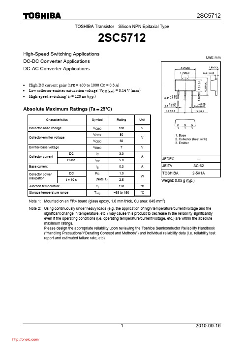
2SC5712(TE12L,F);中文规格书,Datasheet资料
♦: Single nonrepetitive pulse
Ta = 25°C 0.1 Note that the curves for 100 ms*,
10 s* and DC operation* will be
different when the devices aren’t
mounted on an FR4 board (glass
Unit: mm
• High DC current gain: hFE = 400 to 1000 (IC = 0.3 A) • Low collector-emitter saturation voltage: VCE (sat) = 0.14 V (max) • High-speed switching: tf = 120 ns (typ.)
Note 2: Using continuously under heavy loads (e.g. the application of high temperature/current/voltage and the significant change in temperature, etc.) may cause this product to decrease in the reliability significantly even if the operating conditions (i.e. operating temperature/current/voltage, etc.) are within the absolute maximum ratings. Please design the appropriate reliability upon reviewing the Toshiba Semiconductor Reliability Handbook (“Handling Precautions”/“Derating Concept and Methods”) and individual reliability data (i.e. reliability test report and estimated failure rate, etc).
2SA系列(PNP型)三极管全参数表

硅 PNP 三极管
95
HITACHI
硅 PNP 三极管,低频放大,配对管 2SC458/2SC2308
-100m
300m
-30
HITACHI
硅 PNP 三极管,低频放大,配对管 2SC458/2SC2308
-100m
300m
-30
锗 PNP 三极管,高频射频放大
60m -10m -40
HITACHI
-180
80M 30-320
3CA10F
-200
80M 30-320
3CA10F
-250 -150
-100
80M 30-320 40-200
3CA10F 3CD8E 3CD8E 3CA5F
-350
10
-400 -100
10 15M
20-200
3AG95A 3CA10F
-160 120M 60-200
硅 PNP 三极管
硅 PNP 三极管
-100m
400m
-60
-200m 250m
-200m 250m
2SA1028 2SA1029 2SA1029B 2SA103 2SA1030 2SA1030B 2SA1030C 2SA1031 2SA1031C 2SA1031D 2SA1032 2SA1032B 2SA1032C 2SA1033
PANASONIC 硅 PNP 三极管,低频放大,配对管 2SC2295
硅 PNP 三极管
200m -30m -30
-100m
250m
-70
2SA1024
硅 PNP 三极管
-100m 400m
2SA1025 2SA1026 2SA1027
- 1、下载文档前请自行甄别文档内容的完整性,平台不提供额外的编辑、内容补充、找答案等附加服务。
- 2、"仅部分预览"的文档,不可在线预览部分如存在完整性等问题,可反馈申请退款(可完整预览的文档不适用该条件!)。
- 3、如文档侵犯您的权益,请联系客服反馈,我们会尽快为您处理(人工客服工作时间:9:00-18:30)。
DC CURRENT GAIN vs. COLLECTOR CURRENT
1 000 VCE = 3 V
DC Current Gain hFE
100
10 0.1
1
10
100
Collector Current IC (mA)
4
Data Sheet PU10082EJ02V0DS
2SC5617
GAIN BANDWIDTH PRODUCT vs. COLLECTOR CURRENT
2SC5617
ELECTRICAL CHARACTERISTICS (TA = +25°C)
Parameter DC Characteristics Collector Cut-off Current Emitter Cut-off Current DC Current Gain RF Characteristics Gain Bandwidth Product Insertion Power Gain Noise Figure Reverse Transfer Capacitance fT S21e NF Cre
ORDERING INFORMATION
Part Number 2SC5617 2SC5617-T3 Quantity 50 pcs (Non reel) 10 kpcs/reel Supplying Form • 8 mm wide embossed taping • Pin 2 (Base) face the perforation side of the tape
14 12 10 8 6 4 2 0 1
VCE = 3 V f = 2 GHz
10 Collector Current IC (mA)
100
Data Sheet PU10082EJ02V0DS
5
2SC5617
INSERTION POWER GAIN, MAG, MSG vs. FREQUENCY
Insertion Power Gain |S21e|2 (dB) Maximum Available Power Gain MAG (dB) Maximum Stable Power Gain MSG (dB)
VCE = 2 V f = 2 GHz
10 Collector Current IC (mA)
100
10 Collector Current IC (mA)
100
GAIN BANDWIDTH PRODUCT vs. COLLECTOR CURRENT
16
Gain Bandwidth Product fT (GHz)
Document No. PU10082EJ02V0DS (2nd edition) Date Published March 2002 CP(K) Printed in Japan
The mark • shows major revised points.
© NEC Corporation 2001 © NEC Compound Semiconductor Devices 2002
VCE = 3 V, IC = 10 mA, f = 2 GHz VCE = 3 V, IC = 10 mA, f = 2 GHz VCE = 3 V, IC = 3 mA, f = 2 GHz, ZS = Zopt VCB = 3 V, IE = 0 mA, f = 1 MHz
– 7.0 – –
12.0 8.5 1.5 0.4
INSERTION POWER GAIN, MAG, MSG vs. FREQUENCY
Insertion Power Gain |S21e|2 (dB) Maximum Available Power Gain MAG (dB) Maximum Stable Power Gain MSG (dB)
Note 2 2
Symbol
Test Conditions
MIN.
TYP.
MAX.
Unit
ICBO IEBO hFE
Note 1
VCB = 5 V, IE = 0 mA VEB = 1 V, IC = 0 mA VCE = 3 V, IC = 10 mA
– – 75
– – –
100 100 140
nA nA –
100 10 1 0.1 0.01 0.001 VCE = 2 V
Collector Current IC (mA)
0.0001 0.4
0.5
0.6
0.7
0.8
0.9
1.0
0.0001 0.4
0.5
0.6
0.7
0.8
0.9
1.0
Base to Emitter Voltage VBE (V)
Base to Emitter Voltage VBE (V)
Collector to Base Voltage VCB (V)
COLLECTOR CURRENT vs. BASE TO EMITTER VOLTAGE
100 10 1 0.1 0.01 0.001 VCE = 1 V
Collector Current IC (mA)
COLLECTOR CURRENT vs. BASE TO EMITTER VOLTAGE
35 30 25 20 15 10 |S21e|2 5 0 0.1 1 Frequency f (GHz) MSG MAG
VCE = 1 V IC = 10 mA
35 30 25 20 15 10 5 0 0.1 1 Frequency f (GHz) |S21e|2 MSG MAG
VCE = 2 V IC = 10 mA
300
Total Power Dissipation Ptot (mW)
250 200 150
Mounted on Glass Epoxy PCB (1.08 cm2 × 1.0 mm (t) )
140
100 50
0
25
50
75
100
125
150
0
1
2
3
4
5
6
7
8
9
Ambient Temperature TA (˚C)
40
Collector Current IC (mA)
30
20
ቤተ መጻሕፍቲ ባይዱ
300 µ A 270 µ A 240 µ A 210 µ A 180 µ A 150 µ A 120 µ A 90 µ A 60 µ A 2 4 IB = 30 µ A 6 8
10
0.0001 0.4
0.5
0.6
0.7
0.8
0.9
1.0
Note
Ratings 9.0 6.0 2.0 30 140 150 −65 to +150
Unit V V V mA mW °C °C
Tj Tstg
2 Note Mounted on 1.08 cm × 1.0 mm (t) glass epoxy PCB
Because this product uses high-frequency technology, avoid excessive static electricity, etc.
10
10
INSERTION POWER GAIN, MAG, MSG vs. FREQUENCY
Insertion Power Gain |S21e|2 (dB) Maximum Available Power Gain MAG (dB) Maximum Stable Power Gain MSG (dB)
– – 2.5 0.7
GHz dB dB pF
Notes 1. Pulse measurement: PW ≤ 350 µs, Duty Cycle ≤ 2% 2. Collector to base capacitance when the emitter grounded
hFE CLASSIFICATION
The information in this document is subject to change without notice. Before using this document, please confirm that this is the latest version.
Not all devices/types available in every country. Please check with local NEC Compound Semiconductor Devices representative for availability and additional information.
16
Gain Bandwidth Product fT (GHz)
GAIN BANDWIDTH PRODUCT vs. COLLECTOR CURRENT
16
Gain Bandwidth Product fT (GHz)
14 12 10 8 6 4 2 0 1
VCE = 1 V f = 2 GHz
14 12 10 8 6 4 2 0 1
DC CURRENT GAIN vs. COLLECTOR CURRENT
DC Current Gain hFE
100
DC Current Gain hFE
1 10 100
100
10 0.1
10 0.1
1
10
100
Collector Current IC (mA)
Collector Current IC (mA)
Rank Marking hFE Value EB Y1 75 to 110 FB Y2 95 to 140