FINAL_BDTI_MIPS_74k
角度ков里元 com 过电安全意识系踋 18.01.21 的用户指南 (zh-TW)说明书
Bosch Sicherheitssysteme GmbH
Configuration Manual
目錄 | zh-TW 5
57 58 58 59 59 59 60 60 61 62 62 63 64 64 66 67 68 68 69 69 69 69 70 71 71 71 73 73 74 76 76 76 78 79 79 80 81 82 83 83 84 85 87 88 88 88 89 89 90
編輯編碼器 / 編輯解碼器對話方塊 管理真實性驗證 設置驗證 上傳憑證 下載憑證 在工作站上安裝憑證 提供解碼器的目的地密碼 (驗證...) 變更編碼器 / 解碼器的密碼 (變更密碼 / 輸入密碼) 從更換的編碼器復原錄影 (與前身的錄影建立關聯) 設置編碼器 / 解碼器 設置多個編碼器 / 解碼器 錄影管理頁面 錄影偏好設定頁面 設置多點傳播 地圖與結構頁面 連續畫面產生器對話方塊 新增連續畫面對話方塊 新增連續畫面步驟對話方塊 設置「邏輯樹狀結構」 設置「邏輯樹狀結構」 新增服務至「邏輯樹狀結構」 移除樹狀結構項目 管理預先設置的攝影機連續畫面 新增攝影機連續畫面 新增資料夾 設置略過裝置 攝影機與錄影 頁面 攝影機 頁面 PTZ/ROI 設定對話方塊 設置攝影機與錄影設定 設置 PTZ 連接埠設定 設置 PTZ 攝影機設定 使用者群組 頁面 使用者群組屬性 頁面 使用者屬性 頁面 登入組屬性 頁面 攝影機權限 頁面 LDAP 伺服器設定對話方塊 邏輯樹狀結構 頁面 操作員功能頁面 使用者介面 頁面 帳戶原則頁面 設置使用者、權限與企業存取功能 建立群組或帳戶 建立標準使用者群組 建立使用者 建立雙授權群組 在雙授權群組中新增登入組 設置系統管理群組
使用者介面的文字以粗體標示。 4 箭頭請您按一下劃有底線的文字,或按一下應用程式中的項目。
DPtech DPX8000 系列深度业务网关用户配置手册统一审计网关业务板
iii
DPtech DPX8000 系列深度业务交换网关用户配置手册统一审计网关分册 ----------------------------------------------------------------------------------------------------------------------------------------------------
目
录
UAG 插卡部分.................................................................................................................................................. 2 2 ..................................................................................................................................................2 第 1 章 防病毒.................................................................................................................................................. 2 1.1 简介..............................................................................................................................
hcAT91 CPU card 说明书
hcAT91 CPU card User ManualRevision: 1.0© 2004 Andras Tantos and Modular Circuits.All rights reserved.IntroductionThe hcAT91 CPU card is a member of the H-Storm system CPU card family. The H-Storm project is a modular system-level design approach targeting hobby electronics, robotics and fast prototyping. The project defines a standard 72-pin connector as the interconnect between the various elements of the system with two optional 20-pin extension connectors. The elements of an H-Storm system are CPU cards, peripherial cards and system-boards. For detailed information on the H-Storm project please see the H-Storm System Manual available from the H-Storm website.The hcAT91 CPU card is a standard H-Storm system component and is built around the ATMEL AT91R40008 microcontroller. That device integrates a 66MHz ARM7TDMI processor core with 256kBytes of on-chip SRAM and a wide set of peripherials. The processor employs a 32-bit internal and a 16-bit external bus architecture.The CPU card combines this microcontroller with a 16-bit FLASH ROM of up to 8MByte in size, and some support circuitry.The low power microcontroller is run on 1.8V core and 3.3V I/O power supply voltages. The core power can be produced on-board by a small LDO regulator or provided externally.The processor module can be programmed in a variety of languages using the GNU toolchain, like C/C++ Pascal or ADA. There are also several other commercial development tools available from many vendors.© 2004 Andras Tantos, Modular Circuits Rev: 1.0hcAT91 CPU card User ManualTable of Contents Introduction (2)Features (3)License (3)H-Storm Non-Commercial license (HSNCL) (3)Theory of operation (4)System-bus (4)Integrated peripherials (5)PnP Bus (6)Programming mode (6)Power considerations (6)H-Storm module connector pin-out (7)Mechanical design (7)Electrical design (7)Features•66MHz ARM7TDMI processor core•256kb zero wait-state RAM•Up to 8MBytes of 16-bit FLASH memory (2MB standard)• A user-programmable LED to display program state• A watch-dog LED that lights up if a watch-dog event occurred•Optional internal core power supply•8-bit or 16-bit external bus operations are supported•Versatile bus-interface with programmable speed for each different peripherial slot•Two serial ports•Three timer/counters•Up-to 22 digital I/O lines (27 in non-H-Storm compatible mode)•JTAG debug interface provided•Can boot from internal FLASH or from external memory connected to nSEL0•On-board reset generatorLicenseThis document and all the accompanying design documentation (for example schematic and PCB files) are covered by the H-Storm Non-Commercial License (HSNCL).H-Storm Non-Commercial license (HSNCL)Copyright 2004 Andras Tantos and Modular Circuits. All rights reserved.Redistribution and use in source or binary forms, or incorporated into a physical (hardware) product, with or without modification, are permitted for non-commercial use only, provided that the following conditions are met:•The redistribution doesn't result in financial gain.•Redistributions of source code must retain the above copyright notice, this list of conditions and the following disclaimer.3LicensehcAT91 CPU card User Manual Rev: 1.0© 2004 Andras Tantos, Modular Circuits •Redistributions in any other form must contain in printed or electronical format the above copyright notice, this list of conditions and the following disclaimer in the documentation and/or other materials provided with the distribution.•All advertising materials mentioning features or use of this technology must display the following acknowledgment:This product includes H-Storm technology developed by Andras Tantos and Modular Circuits.•Neither the name of Andras Tantos or Modular Circuits may be used to endorse or promote products derived from or using this technology without specific prior written permission.ALL THE INFORMATION, TECHNOLOGY, AND SOFTWARE IS PROVIDED BY THE AUTHORS ``AS IS'' AND ANY EXPRESS OR IMPLIED WARRANTIES, INCLUDING, BUT NOT LIMITED TO, THE IMPLIED WARRANTIES OF MERCHANTABILITY AND FITNESS FOR A PARTICULAR PURPOSE ARE DISCLAIMED. IN NO EVENT SHALL ANDRAS TANTOS, MODULAR CIRCUITS OR CONTRIBUTORS BE LIABLE FOR ANY DIRECT, INDIRECT, INCIDENTAL, SPECIAL, EXEMPLARY, OR CONSEQUENTIAL DAMAGES (INCLUDING, BUT NOT LIMITED TO, PROCUREMENT OF SUBSTITUTE GOODS OR SERVICES; LOSS OF USE, DATA, OR PROFITS; OR BUSINESS INTERRUPTION) HOWEVER CAUSED AND ON ANY THEORY OF LIABILITY, WHETHER IN CONTRACT, STRICT LIABILITY, OR TORT (INCLUDING NEGLIGENCE OR OTHERWISE) ARISING IN ANY WAY OUT OF THE USE OF THIS SOFTWARE OR TECHNOLOGY, EVEN IF ADVISED OF THE POSSIBILITY OF SUCH DAMAGE.Theory of operationThe hcAT91 module contains three main components and some additional support circuitry. The tree main components are the AT91R40008 microcontroller, the 16-bit FLASH memory and the 72-pin H-Storm standard connector.System-busThe integrated memory-controller of the microcontroller is used to address the three available peripherial regions (nSEL0, nSEL1, nSEL2) and the FLASH memory. All I/O regions are mapped to memory locations. The mapping between these signals and the microcontrollers' external chip-selects under normal operation is asTheory of operation4© 2004 Andras Tantos, Modular Circuits Rev: 1.0hcAT91 CPU card User Manual Since the microcontroller boots from external memory connected to CS0, this change makes it possible to boot the processor from either the internal FLASH memory for normal operation or from an external memory connected to nSEL0 for initial programming purposes.Upon reset the microcontroller starts execution of the program found in a memory connected to CS0. This memory is initially mapped to physical address 0. The execution starts in ARM mode. The memory access cycles are programmed to be rather slow so that all types of FLASH devices would be compatible with the processor. After the initial program startup, the application can program faster accesses to CS0 to better match the capabilities of the FLASH memory, switch to THUMB mode to better facilitate the narrow 16-bit external bus, or copy itself into internal RAM where it can be executed full-speed with zero wait-states.Additional chip-select signals (CS1-CS3) are used to access the H-Storm peripherial and the system-board. These chip-select signals can be assigned to arbitrary physical memory locations to better suite the application needs and are highly programmable so that various communication speeds can be used with different peripherials.The CPU module supports both 8-bit and 16-bit access cycles, with and without wait-states. It does not generate burst cycles.The module support both edge- and level-triggered interrupts. The nIRQx lines of the H-Storm connector areIntegrated peripherialsThe microcontroller contains three timers/counters, two serial ports, a watch-dog timer and 32-bit GPIO lines. Many of these lines however are multiplexed to the same pins of the processor chip. All of the available peripherials are connected to the H-Storm bus, with the exception of a couple of the GPIO lines. The user-5Theory of operationhcAT91 CPU card User Manual Rev: 1.0© 2004 Andras Tantos, Modular CircuitsPnP BusThe H-Storm PnP bus signals are connected to two GPIO lines of the microcontroller. The protocol of the PnP bus is implemented in SW. The pin assignment is as follows:Programming modeWhen the nPROG signal is tied low upon reset, the microcontroller will boot from an external memory connected to nSEL0 for initial programming purposes. This allows for program execution on a module where the on-board flash is corrupted or simply blank. The external memory can contain code that erases and re-programs the FLASH memory such that consequent boot attempts from that memory would succeed. Since the standard H-Storm bus is capable of accessing only 2kBytes of external memory connected to any single peripherial select signal, only a very small boot-loader program can be placed in that external memory. The usual method therefore would be that that small boot-loader would download a bigger binary image from a host computer by means of one of the serial ports of the microcontroller. This larger program would than be capable of initializing the FLASH memory to a valid state and program a boot-image into it.When the nPROG signal is high upon reset, normal boot-sequence from the on-board FLASH memory us used. Power considerationsTwo versions of the module exist. One contains an integrated 1.8V voltage regulator and requires only a single power source of 3.3V. The other does not contain this integrated power supply and relies on dual 3.3V/1.8V external power. The power consumption of the module under various circumstances is as follows:Theory of operation6© 2004 Andras Tantos, Modular Circuits Rev: 1.0hcAT91 CPU card User ManualH-Storm module connector pin-out7H-Storm module connector pin-outhcAT91 CPU card User Manual Rev: 1.0© 2004 Andras Tantos, Modular CircuitsH-Storm module connector pin-out8© 2004 Andras Tantos, Modular Circuits Rev: 1.0hcAT91 CPU card User ManualMechanical designThe module adheres to the H-Storm standard module specification. It is 100mm wide and 47.5mm high. It is implemented on a standard double-sided 1.5mm laminate PCB process with 0.5mm via hole size and 0.2mm track width.9Mechanical design。
V7000招标参数

V7000招标参数V7000招标参数标准格式文本一、项目背景随着信息技术的快速发展,存储设备在各行各业中的需求也日益增长。
为了满足公司业务的存储需求,我们计划进行V7000存储设备的招标采购。
为了确保招标过程的公平、公正和透明,制定本文档,明确V7000招标参数的标准格式。
二、招标参数1. 存储容量- 最小存储容量:500TB- 最大存储容量:1PB- 存储容量扩展性:支持动态扩展,最小扩展容量为100TB2. 存储性能- IOPS(每秒输入/输出操作数):最小100,000 IOPS- 带宽:最小10GB/s- 响应时间:最大10毫秒3. 存储接口- 支持Fibre Channel接口:最小16个端口- 支持Ethernet接口:最小8个端口- 支持SAS接口:最小8个端口4. 存储可靠性- RAID级别:支持RAID 0、1、5、6、10- 磁盘故障容忍度:支持多个磁盘故障容忍- 数据保护:支持快照、复制、镜像等功能5. 存储管理- 管理界面:提供易于使用的图形用户界面(GUI)- 远程管理:支持通过网络远程管理存储设备- 存储资源管理:支持存储池、卷、逻辑单元等资源的管理6. 兼容性- 操作系统兼容性:支持主流操作系统,如Windows、Linux、UNIX等- 虚拟化兼容性:支持主流虚拟化平台,如VMware、Hyper-V等- 数据库兼容性:支持主流数据库系统,如Oracle、SQL Server等7. 服务支持- 售后服务:提供7x24小时的售后技术支持- 维修响应时间:提供4小时内的维修响应时间- 软件升级:提供定期的软件升级服务三、评分标准为了确保招标过程的公正和客观,制定以下评分标准:1. 存储容量:满足最小存储容量要求得10分,每增加100TB加1分,最高得分为20分。
2. 存储性能:满足最小IOPS和带宽要求得10分,每增加10,000 IOPS和1GB/s加1分,最高得分为20分。
八线4X SDR InfiniBand 端口交换平台用户手册说明书
Eight 4X SDR InfiniBand Port Switch PlatformUser’s ManualPart Number: F-X430066Rev 1.012Eight 4X SDR InfiniBand Port Switch Platform User’s Manual3 ContentsContents 3List of Figures 5 Revision History 7 About this Manual 9 Chapter 1 Overview 11 Chapter 2 Installation and Basic Operation 122.1 Switch Platform Hardware Overview 122.1.1 InfiniBand Connectors 132.1.2 InfiniBand Port LEDs 132.1.3 System Status Indicators 132.1.4 I2C-compatible Bus Connector 132.2 Switch Platform Installation and Operation 132.2.1 Mechanical Installation 142.2.2 Power Connections and Initial Power On 142.2.3 InfiniBand Copper Cable Installation 142.2.3.1 Cable Length Support And IB Port Configuration 15 Chapter 3 Management Tools Overview 163.1 Updating Firmware 163.2 IB Administration 163.2.1 IBADM Requirements 173.2.2 How to Get IBADM 17 Appendix A Specification19 Appendix B Mechanical Drawing20 Appendix C Rack Adapter Installation Instructions21Rev 1.014Rev 1.01Eight 4X SDR InfiniBand Port Switch Platform User’s Manual5 List of FiguresFigure 1: Switch Front and Rear Panels12 Figure 2: Default Configuration Model (Example)16 Figure 3: Switch, Mounting Ears, Screws21 Figure 4: Rear Panel Side with Ear Screws Removed22 Figure 5: Mounting Ear Assembled on Rear Panel Side22 Figure 6: View of Rack Adapter Assembled on Rear Panel Sides23 Figure 7: View of Rack Adapter Assembled on Front Panel Sides23Rev 1.016Rev 1.01Eight 4X SDR InfiniBand Port Switch Platform User’s Manual7 Revision HistoryTable 1 - Revision History TableRevision & Date Description1.01 March 2006Added warnings to Section2.2.2, “Power Connections and Initial Power On,” on page141.00 February 2006First versionRev 1.018Rev 1.01Eight 4X SDR InfiniBand Port Switch Platform User’s Manual9 About this ManualThis manual provides an overview of the Eight 4X SDR InfiniBand Port Switch system and guidelines for its opera-tion. Specifically, it covers the following product:Table 1 - Switch Products Covered in this User’s ManualProduct Number DescriptionF-X430066Eight 4X InfiniBand Port Switch PlatformIntended AudienceThis manual is intended for users and system administrators responsible for installing and setting up the switch plat-form listed above.The manual assumes familiarity with the InfiniBand™ architecture specification.Rev 1.0110Rev 1.01Eight 4X SDR InfiniBand Port Switch Platform User’s Manual11 1 OverviewThis User’s Manual provides an overview of the Eight 4X InfiniBand Port Switch System based on Mellanox Tech-nologies’ MT43132 InfiniScale switch device.The switch platform comes pre-installed with all necessary firmware and configuration for standard operation in an InfiniBand fabric running an InfiniBand compliant Subnet Management software in the subnet. All that is requiredfor normal operation is to follow the usual precautions for installation and connection to the fabric. Once connected, the Subnet Management software automatically configures and begins utilizing the switch.Basic installation and hardware maintenance is covered in “Installation and Basic Operation” on page12. Maintenance and configuration of the switch is done In-Band through the InfiniBand fabric using the IBADM tools package. This package provides the ability to monitor the temperature, voltage, port utilization, and other status parameters in the switch. To upgrade switch firmware, the MFT package is required. See “Management Tools Over-view” on page16.Installation and Basic Operation122 Installation and Basic Operation2.1 Switch Platform Hardware OverviewFigure 1 shows the front and rear panel views of the Eight 4X Ports Switch System, including the I 2C connector and status LEDs.Rear PanelI2C-compatible BusConnectorFront PanelStatusLEDsIB Port 8IB Port 1Figure 1: Switch Front and Rear PanelsLink LEDEight 4X SDR InfiniBand Port Switch Platform User’s Manual132.1.1 InfiniBand ConnectorsAll InfiniBand connectivity is via the rear panel. Figure1 shows the eight 4X InfiniBand port connectors. Each port also includes power supply functionality to support fiber media adapters.2.1.2 InfiniBand Port LEDsTwo IB port LEDs are located to the left of each IB port connector on the rear panel (see Figure1 on page12). The lower (Green) LED is the IB port Physical link LED, and the upper (Yellow) LED is the IB port Logical link LED (Activity LED).Physical Link LED (Green) indications:•Steady On:The Physical link is established•Off:Physical link error, poor connection quality, or no physical connectionActivity LED (Yellow) indications:•Steady On:The Logical link is up but there is no data transfer•Blinking:Data is being transferred to/from the switch port across the cable wires•Off:The Logical link is down2.1.3 System Status IndicatorsTwo system status indicators are located on the left of the rear panel and are labeled “Status” (see Figure1 onpage12). The following status conditions are possible:1.SYSTEM STATUS OK: Green ON, Yellow OFF2.TEMPERATURE ALARM: Yellow ON3.SYSTEM OFF: Green OFF, Yellow OFF4.POWER CIRCUIT ERROR: Green OFF, Yellow OFF (with the power cord connected to power)2.1.4 I2C-compatible Bus ConnectorThe I2C-compatible Bus connector is for factory and development use only.The connector is a female 9 pin D-Type connector. Table1 shows the pinout functions:Table 1 - I2C-compatible Bus Connector Pinout FunctionsPin Number Function1-5GND6SDA8SCL7, 9Not Connected2.2 Switch Platform Installation and OperationInstallation and initialization of the switch platform are straightforward processes, requiring attention to the normal mechanical, power, and thermal precautions for rack-mounted equipment. The switch platform does not require any programming or configuration to operate as a basic InfiniBand switch and includes all of the necessary functionality to operate with external standard InfiniBand Subnet Management software.Installation and Basic Operation14This section describes the installation process and basic operation of the switch platform.2.2.1 Mechanical InstallationThe switch platform is packaged in a 1U chassis. See Table 2, “Switch Platform Mechanical and Environmental Requirements (Worst Case, Fully Populated Chassis)”. If the switch is to be mounted in a standard 19” rack it will require an adapter. Two ear brackets are included (but not assembled) in the packing box of the switch system, which can be assembled on the sides of the chassis acting as the 19” rack adapter, and include rack mounting holes which conform to the IEA-310 standard for such a rack. See “Rack Adapter Installation Instructions” on page 21.Note:The installer should use a rack cable to support the mechanical and environmental charac-teristics of a fully populated switch Chassis as listed in Table 2.Proper ventilation should also be guaranteed for air intake at the front of the chassis and exhaust at the rear in order to maintain good airflow at ambient temperature. Cable routing in particular should not impede the air exhaust from the chassis.Note that the switch platform can be either front or rear mounted. The notion of “front” and “rear” is arbitrary; how-ever, “rear” is used consistently in this manual to refer to the side of the chassis with the InfiniBand connectors.2.2.2 Power Connections and Initial Power OnWarning: The switch platform will automatically power on when AC power is applied. There is no power switch. Make sure the power cable is properly plugged into the system before connecting to power.Warning: The switch platform must be connected to an earthed mains socket-outlet.Warning: In Norway, this system should be connected to the IT power distribution system only .The input voltage is auto-adjusting for a 100-240 V AC, 50-60Hz power connection. The power cord should be a stan-dard 3-wire AC power cord including a safety ground and rated for 2A or higher.2.2.3 InfiniBand Copper Cable InstallationThe switch platform uses industry standard 4X InfiniBand cables which are available from several vendors. The stan-dard 4X cables support full-duplex 10Gb/s wire speed for all switch platform ports. All cables can be inserted or removed with the unit powered on. To insert a cable, press the connector onto the port receptacle until the connector is firmly seated. The GREEN LED indicator to the left of each port will light when the physical connection is estab-lished (that is, when the unit is powered on and a cable is plugged into the port with a functioning port plugged into the other end of the connector). After plugging in a cable, lock the connector using the latching mechanism particular to the cable vendor. To remove, disengage the locks and slowly pull the connector away from the port receptacle. Both LED indicators will turn off when the cable is unseated.Table 2 - Switch Platform Mechanical and Environmental Requirements (Worst Case, Fully Populated Chassis)Rack HeightRack Width Rack Depth Weight Power Ambient Temp.1U12.4”(315mm)w/o Rack Adapter 6.9”(175mm)7.7lb (3.5Kg)45WSingle 100-240 V AC 50-60HzInputMax: 50ºC Min: 0ºC19” (EIA-310)(483mm)w/ Rack AdapterEight 4X SDR InfiniBand Port Switch Platform User’s Manual15Warning:Care should be taken not to impede the air exhaust flow through the ventilation next to the InfiniBand ports. Cable lengths should be used which allow for routing horizontally around to the side of the chassis before bending upward or downward in the rack.2.2.3.1 Cable Length Support And IB Port ConfigurationThe switch platform is configured to drive cables up-to 20 meters long. This configuration allows maximum flexibil-ity in building a robust IB cluster.The selected configuration and cables should meet the required BER specified in the InfiniBand Architecture Specifi-cation, Volume 2, release 1.2.Management Tools Overview 163 Management Tools Overview3.1 Updating FirmwareIn order to update switch firmware, the MFT tools package is needed by Mellanox Technologies. To download this package, visit /support/switch_firmware_table.php. Make sure to also download the MFT User’s Manual and Release Notes. Specifically, the ‘spark’ tool of the MFT package is required for firmware updates. Please see the MFT User’s Manual for details.The most updated firmware is also available for download from the same web page above. Please find the ‘Custom Switch based on Mellanox's MT43132 InfiniScale switch device’ entry in the firmware table.3.2 IB AdministrationTo monitor status conditions in the switch platform, the IBADM tools package is needed (by Mellanox Technolo-gies). IBADM enables the system administrator to manage one or more switch platforms from a single remote Infini-Band host. The features include the following:•Full In-Band Management of Multiple Switch and HCA Systems from single host1•Simple default configuration to get started quickly•Name-based subnet browsing and topology verification•Event monitoring of port statistics, link status and system status for all ports in the switch•Checking and updating the firmware•Intuitive CLI interface•Extensible and customizableThe figure below shows the default configuration model for these tools:Figure 2: Default Configuration Model (Example)One or more switches InfiniBand HCA1.Firmware updates to this Eight 4X IB Port Switch System cannot be performed using ibfwmgr (the burning tool of IBADM pack-age). See Section3.1, “Updating Firmware,” on page16.Eight 4X SDR InfiniBand Port Switch Platform User’s Manual173.2.1 IBADM RequirementsThe general requirements for installing the IBADM software are listed below. Please see the IBADM release notesfor details on platform, OS, Driver and Subnet Management support.puter Platform with an InfiniBand HCA card installed12.HCA Driver3.InfiniBand Compliant Subnet Management. The Open Source SM (Eponyms) is supported.3.2.2 How to Get IBADMPlease visit Mellanox Technologies’s Documents Distribution System at . The IBADM package is available for download under ‘Code Releases/ Tools’. Note that access requires a customer login account. Consult your sales representative for details.1.Any Mellanox Technologies HCA card can be used. Consult your sales representative for other possibilities.Management Tools Overview 18Eight 4X SDR InfiniBand Port Switch Platform User’s Manual19 Appendix A: SpecificationTable 3 - Specification DataPhysical Power and EnvironmentalSize (HxDxW): Size with Rack AdapterWeight:Mounting: 10Gb/s Connector:1U x 6.9” x 12.4” (43.6mm x 175mm x 315mm)1U x 6.9” x 19” (43.6mm x 175mm x 482.6mm)7.7lb (3.5kg)19” RackmountInfiniBandInput V oltage:Maximum Power:Ambient Temperature:Humidity:Altitude:Shock:Vibration:Internal V oltage:100-240 V AC 50-60Hz45W0ºC to 50ºC10% - 90% non-condensing+5 VDCProtocol Support Regulatory ComplianceInfiniBand:QoS: RDMA Support: Management:10Gb/s8 InfiniBand Virtual Lanes for all portsYes, All PortsPerformance, and Device managementAgents for full InfiniBand In-Band Manage-mentSafetyEMCScalability and Performance Reliability, Availability and Serviceability FeaturesSwitching Performance:Addressing:Simultaneous wire-speed any port to any port48K Unicast Addresses Max. per Subnet16K Multicast Addresses per SubnetHot-Swappable:N+1 Redundant:NoneNone20Appendix B: Mechanical Drawing21Appendix C: Rack Adapter Installation InstructionsC.1 Rack Adapter Assembly PartsThe rack adapter assembly parts are included in the switch packing box and are listed in Table 4:C.2 Assembling the Rack AdapterSTEP 1:Remove the pair of screws from the two sides of the chassis where the rack adapter is to be installed. See Figure 4 on page 22.Note: The rack adapter can be installed on the sides close to the front panel or to the rear panel.Table 4 - Rack Adapter Assembly PartsItem QuantityNotes Mounting Ear2See Figure 3Phillips 100° Flat Head, Passivated Stainless SteelUNC Screw 4-40 x ¼2Each mounting ear requires 3 screws. Two additional pairs ofscrews are to be found assembled on the switch chassis sides.Figure 3: Switch, Mounting Ears, ScrewsSTEP 2:Assemble the rack kit as shown in Figure 5.See also Figure 6,“View of Rack Adapter Assembled on Rear Panel Sides” and Figure 7, “View of Rack Adapter Assembled on Front Panel Sides,” on page23.Figure 4: Rear Panel Side with Ear Screws RemovedFigure 5: Mounting Ear Assembled on Rear Panel Side23Figure 6: View of Rack Adapter Assembled on Rear Panel SidesFigure 7: View of Rack Adapter Assembled on Front Panel Sides。
机房和施工组织模板

江西新昌电厂“上大压小〞新建工程厂级管理信息系统〔MIS〕网络及硬件平台系统集成投标文件投标编号:03-ct-03-2007-156〔第三卷附件1-技术标准书〕投标人:安徽科大恒星电子商务技术二00九年四月目录第一章概述 (1)工程建设需求 (1)设计原那么 (2)实用性与先进性相结合 (2)可扩展性和开放性 (2)可靠性和平安性 (3)可管理性 (3)设计、施工标准 (3)工程建设目标 (6)第二章效劳器系统平台设计 (7)建设需求 (7)数据库效劳器设计 (7)IBM power550方案 (7)效劳器选型 (7)2.2.1.2 IBM Power 550配置 (12)HP 小型机方案 (13)效劳器选型 (13)2.2.2.2 HP Integrity rx6600 配置 (17)系统运行模式设计 (17)并行处理模式 (18)任务分担模式 (18)主机备用模式 (18)其它效劳器设计 (18)效劳器的部署 (18)物理效劳器与逻辑效劳器之间的关系 (19)效劳器选型设计 (20)2.3.3.1 IBM X3850 M2方案 (20)2.3.3.2 HP ProLiant DL580 G5 效劳器方案 (23)效劳器配置 (26)2.3.4.1 IBM X3850 M2配置 (26)2.3.4.2 HP ProLiant DL580 G5配置 (27)SAN存储系统设计 (27)2.4.1 IBM TotalStorage DS4800方案 (28)2.4.1.1 IBM TotalStorage DS4800介绍 (28)2.4.1.2 TotalStorage DS4800配置 (31)2.4.2 HP StorageWorks EVA8100方案 (32)2.4.2.1 HP StorageWorks EV A8100介绍 (32)2.4.2.2 HP StorageWorks EV A8100配置 (35)光纤交换机选型 (36)2.4.3.1 IBM System Storage SAN2005-B16 特性 (36)2.4.3.2 IBM System Storage SAN2005-B16 配置 (38)数据备份系统 (38)数据备份需求 (38)数据备份方案 (39)2.5.2.1 Veritas的优势 (39)2.5.2.2 Veritas配置 (42)磁带库选型配置 (43)虚拟磁带库选型 (44)第三章网络系统平台设计 (49)网络建设需求 (49)网络拓扑结构设计 (49)分层设计 (49)可靠性保证〔冗余设计〕 (49)网络拓扑实现 (50)核心层设计 (51)接入层设计 (51)远程访问层设计 (51)Cisco解决方案 (51)中心交换机选型 (51)3.3.1.1 Cisco® 6500介绍 (52)3.3.1.2 Supervisor Engine 720 (56)3.3.1.3 Cisco Catalyst 6513配置 (58)接入交换机选型 (59)H3C解决方案 (59)中心交换机选型 (59)H3C S7500E介绍 (60)H3C S7510E配置 (63)接入交换机选型 (63)第四章系统平安设计 (65)系统平安需求 (65)系统平安体系结构 (65)物理设备平安 (65)访问平安 (66)应用平安 (66)数据平安 (66)平安策略 (67)传输通道和传输设备平安 (67)应用平台平安 (68)资源访问平安 (68)网络防病毒 (69)多功能防火墙设计 (70)HillstoneSA-5020介绍 (71)HillstoneSA-5020功能规格 (72)内网核心平安防护系统〔主机加固〕设计 (74)S-NUMEN用途 (74)S-NUMEN功能 (75)S-NUMEN配置 (76)内网主机审计及监管系统 (76)系统功能 (77)系统特点 (79)体系架构 (80)配置 (81)防病毒系统设计 (81)网络防病毒配置 (84)第五章综合布线系统设计 (85)综合布线系统需求 (85)设计标准与设计目标 (85)设计标准 (85)设计目标 (86)布线系统设计 (86)光缆敷设 (86)SAN光纤走向 (86)布线系统测试 (87)测试标准与内容 (89)提交文档 (94)第六章工程组织与管理 (95)工程管理与目标 (95)工程组织及人力资源分配 (96)施工组织总体部署 (96)人力资源配置 (98)与相关单位合作 (99)与工程单位合作 (99)与厂商合作 (100)工程管理 (100)管理方法 (100)管理措施 (101)工程风险管理 (104)工程进度管理 (104)工程质量控制与保证 (105)工程阶段性评估 (106)第七章工程实施方案 (107)工程实施环节规划 (107)实施环节规划总表 (107)设计联络 (109)设备订货及到货 (110)实施现场情况调研 (110)制定详细实施方案 (111)培训 (111)设备验收 (111)查验设备 (111)查验方法 (112)查验报告 (117)系统安装调试 (117)系统调试方案制定 (117)小型机调试 (118)中心交换机调试 (118)边缘交换机调试 (118)中心路由器调试 (119)网管软件调试 (119)主机调试 (119)备份系统调试 (120)系统初验收 (120)试运行 (120)技术文档的提交 (121)系统终验 (121)技术支持与售后效劳 (121)实施进度方案 (121)里程碑事件及考核标准 (122)第八章验收方案与文档 (123)验收测试内容 (123)现场验收测试 (124)文档验收 (126)系统初验收 (126)系统终验 (127)测试方案 (127)测试方法 (127)测试工程 (127)测试方法 (128)工程文档 (129)工程文档内容 (129)工程文档提交方案 (132)第九章机房建设工程 (134)工程简述 (134)电子计算机机房组成及使用面积确定 (134)可维护性设备布置 (135)设计原那么 (135)计算机机房平安分类 (135)建设标准 (137)设计依据 (138)设计依据 (138)设计指标 (140)机柜及机房隔断、装饰设计 (141)机柜 (141)图腾机柜概述 (141)图腾机柜选型 (141)机房隔断 (141)装饰设计 (142)装修材料选材 (142)材料表 (143)吊顶 (143)地面 (144)墙、柱面 (145)门、窗 (145)供配电系统〔含UPS、照明等〕 (146)电气概述 (146)供配电系统 (147)设计标准要求 (147)9.5.2.2 机房配电冗余供电系统 (149)配电设备 (149)UPS系统 (149)UPS选型选型 (149)艾默生“UL33〞系列UPS性能参数 (150)美国“艾默生〞系列UPS特点 (151)电池配置 (151)照明系统设计 (152)普通照明系统设计 (153)应急照明、疏导灯具系统设计 (153)配电线路安装技术 (153)空调系统 (154)空调系统设计 (154)空调设备选型 (154)防雷接地 (154)防雷系统概述 (154)对雷电引入的分析 (155)机房防雷设计 (156)防雷验收及保障 (156)接地系统概述 (156)接地系统解决措施 (157)机房的地线系统 (157)局部等电位连接 (157)抗静电保护地 (157)静电防护 (158)KVM设备及机房布线 (158)KVM设计需求 (158)KVM设计方案说明 (159)环境监控、消防报警及其他相关效劳 (159)环境监控 (159)门禁系统 (159)视频监控 (159)动力环境监控 (159)消防报警 (160)9.9.3 控制台桌椅 (161)灾害处理 (161)机房区防水防护措施 (161)机房给水排水技术 (161)防虫、防鼠害 (162)电磁屏蔽 (162)第一章概述江西新昌电厂网络及硬件平台系统集成工程建设主要包括了网络系统、无线网络覆盖、效劳器系统、存储系统、数据备份系统、微软AD域设计及网络部署、管理及系统软件、MIS终端、智能机房、综合布线等系统,按现代先进技术设计,该系统集成完成后,新昌电厂具有统一的生产MIS系统运行平台,能为其信息化建设提供良好的根底效劳。
ADV7842_cn(HDMI接口芯片)
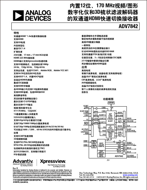
特性
双通道HDMI® 1.4a快速切换接收器 支持HDMI 支持3D电视 内容类型位 兼容CEC 1.4 扩展色度 256引脚、17 mm × 17 mm BGA封装 HDMI 225 MHz接收器 HDMI端口支持Xpressview快速切换 支持3D视频格式,包括帧封装1080p 24 Hz、720p 50 Hz、720p 60 Hz 支持全色度,包括YCC601、Adobe RGB、Adobe YCC 601 支持36/30位深色和24位色彩 支持HDCP 1.4、内置HDCP密钥 自适应HDMI均衡器 集成CEC控制器 支持HDMI中继器 各HDMI端口均支持5 V检测和热插拔 支持HDMI音频,包括HBR和DSD 高级静音特性 灵活的数字音频输出接口 最多支持5个S/PDIF输出 最多支持4个I2S输出 视频/图形数字化仪 4个170 MHz、12位ADC 12通道模拟输入多路复用 525i/625i分量模拟输入 支持525p/625p分量逐行扫描 支持720p/1080i/1080p分量高清电视 针对720p/1080p支持低刷新速率(24 Hz/25 Hz/30 Hz) 可对高达1600 × 1200 、60 Hz (UXGA)的RGB图形进行数字化 处理 支持SCART快速消隐 3D视频解码器 支持NTSC/PAL/SECAM色彩标准 NTSC/PAL 2D/3D运动检测梳状滤波器 包括帧同步的高级时基校正(TBC) 对于525i和625i,支持隔行转逐行 IF补偿滤波器 垂直调峰和水平调峰滤波器 稳定地同步提取质量不佳的视频源 高级VBI数据分隔器 一般特性 高度灵活的36位像素输出接口 针对HDMI和图形的内部EDID RAM 支持双通道STDI(标准识别)功能 任意至任意、3 × 3色彩空间转换(CSC)矩阵 2个可编程中断请求输出引脚 同步模拟处理和HDMI监控
VAR-SOM-MX8M-PLUS based on NXP i.MX 8M Plus Evalua

VAR-SOM-MX8M-PLUS based on NXP i.MX 8M PlusEvaluation Kit Quick Start GuideFeatures:1. Power ON Switch (SW7)2. 12V DC In Jack (J24)3. USB Debug (J29)4. micro SD Card slot (J28)5. USB 3.0 OTG (J26)6. USB 2.0 Host (J23)7. Gigabit Ethernet #0 (J21) 8. Gigabit Ethernet #1 (J20)9. MIPI-CSI #1 Camera connector [optional] (J19) 10. Miscellaneous Header #1 (J17)11. HDMI/ MIPI-CSI #2 Camera connector[optional] (J13)12. Mini PCI Express Connector (J15) 13. Miscellaneous Header #2 (J3) 14. SOM Connector (J1) 15. LVDS#B Header (J5)16. LVDS#A/ DSI Header (J7) 17. Fan Power Connector (J9) 18. Digital Microphone (U1) 19. Resistive Touch (J10) 20. Capacitive Touch (J11)21. User Buttons (SW1, SW2, SW4) 22. Line-In Connector (J12)23. Headphones Connector (J14) 24. Boot Select Switch (SW3)25. SAI/I2C/SPI/CAN Header (J16) 26. Reset Button (SW5)27. PWR Select Switch (SW6) 28. UART/PWM Header (J18) 29. RTC Battery Holder (JBT1)Evaluation kit initial Setup1. Carefully remove the 7” LCD and Symphony-Board from the package.2. Connect the 7” LCD Display and Touch cablesto the Evaluation Kit connectors J7, J11 respectively.Note:connect the display cable with the red wire on pin 1. Connect the touch cable with the metal contacts facing down.3. Plug the USB type A to micro B cable betweenthe USB debug connector (J29) and a PC USB port.4. For heatsink assembly instructions, pleasefollow the VHP-VS8M documentation .Please note that the heatsink is mainly used for CPU/GPU intensive applications and may be required per your specific use case.P/N VSS0177AVAR-SOM-MX8M-PLUS based on NXP i.MX 8M PlusEvaluation Kit Quick Start GuideSetting the host PC for debug1. Download any PC terminal software (e.g. Putty ).2. Set the PC terminal software parameters as follows:- Baud Rate: 115200 - Data bits: 8 - Stop bits: 1 - Parity: None- Flow Control: NoneBooting from eMMC1. Set Boot select switch (SW3) to “Internal” position to boot from the VAR-SOM-MX8M-PLUS internal storage.2. Plug the wall adapter into the 12V power jack (J24) and to a 120VAC~240VAC power source.3. Set Power ON switch (SW7) to ON state.4. Boot messages are printed within the PC terminal window.Booting from a micro SD cardThe microSD card is supplied within the package. Updated SD card images can also be downloaded from the Variscite FTP server.See more details in the recovery SD card section in the Variscite Wiki pages.1. Set Power ON switch (SW7) to off state.2. Set Boot select switch (SW3) to “SD ” positionin order to boot from SD Card.3. Push microSD card into the microSD cardslot (J28) of the Symphony-Board.4. Set Power ON switch (SW7) to ON state.5. Boot messages are print ed within PC’sterminal window.(Re-)Installing the file system to eMMCPlease refer to the recovery SD card section in the Variscite Wiki pages.Linkso Wiki page:https:///index.php?title=VAR-SOM-MX8M-PLUSo VAR-SOM-MX8M-PLUS Evaluation kits:https:///product/evaluation-kits/var-som-mx8m-plus-evaluation-kits/o VAR-SOM-MX8M-PLUS System on Module:https:///product/system-on-module-som/cortex-a53-krait/var-som-mx8m-plus-nxp-i-mx-8m-plus/o Symphony carrier board:https:///product/single-board-computers/symphony-board/o Customer portal:https:///loginThank you for purchasing Variscite’s product.For additional assistance please contact: *******************。
- 1、下载文档前请自行甄别文档内容的完整性,平台不提供额外的编辑、内容补充、找答案等附加服务。
- 2、"仅部分预览"的文档,不可在线预览部分如存在完整性等问题,可反馈申请退款(可完整预览的文档不适用该条件!)。
- 3、如文档侵犯您的权益,请联系客服反馈,我们会尽快为您处理(人工客服工作时间:9:00-18:30)。
MIPS Technologies MIPS32® 74K™Licensable Processor Core© 2007 BDTI ( ). All rights reserved.An Independent Analysis of the:By the staff ofBerkeley Design Technology, Inc.ContentsIntroduction . . . . . . . . . . . . . . . . . . . . . . . . . . . . . . .1About BDTI. . . . . . . . . . . . . . . . . . . . . . . . . . . . . . .2Architecture . . . . . . . . . . . . . . . . . . . . . . . . . . . . . . .2Instruction Set . . . . . . . . . . . . . . . . . . . . . . . . . . . . .4Performance . . . . . . . . . . . . . . . . . . . . . . . . . . . . . . .5Development and Debug Tools. . . . . . . . . . . . . . . .6Conclusions. . . . . . . . . . . . . . . . . . . . . . . . . . . . . . . .6IntroductionMIPS Technologies, Inc. is a provider of licensable, syn-thesizable 32-bit processor cores and other semiconductor design IP . MIPS processors are commonly found in set-top boxes, VoIP SoCs, digital TVs, DVD recorders/players, and networking equipment, applications in which signal pro-cessing is becoming increasingly important. To address applications with combined RISC/DSP demands, MIPS offers 32-bit cores with DSP-oriented hardware and instructions.The first 32-bit MIPS core with significant DSP capabil-ities was the 24KE core, which was introduced in 2005. This core was based on the earlier 24K core but added a set of DSP instruction set extensions, called DSP ASE (Applica-tion Specific Extension) Rev 1, that provided a significant step up in signal processing capabilities. MIPS then intro-duced the 34K core, which also supports the DSP ASE instructions and adds multithreading capabilities.In 2007 MIPS announced the high-performance 74K core. The 74K core is a dual-issue superscalar core that sup-ports MIPS’ next generation of DSP-oriented instruction set extensions, called DSP ASE Rev 2. The 74K core targets demanding multimedia and networking applications, such as WiMaX, DVD players, and VoIP . According to MIPS, the 74K core is fully synthesizable and operates at up to 1.11GHz in a 65 nm process; core details are shown in Table 1.The 74K core can include an optional floating-point unit; if this unit is included the core is called the 74Kf. According to MIPS, the 74K core has been delivered to initial licensees.TABLE 1. fabricated in TSMC 65 nm process using standard cells (nostructured or hard IP). Die area is for the core plus 32K instruction cache and 32K data cache. (Data is courtesy of MIPS, and has not been verified by BDTI.)CoreImplementationMax. Clock Speed Die AreaHigh-Performance 1.11 GHz 2.5mm^2Area-Efficient830 MHz2.1mm^2O VERVIEWMIPS Technologies, Inc. is a provider of semiconductor IP , including processor architectures and IP cores based on these architecture. The company offers a range of licensable 32-bit processor cores for use by SoC designers. These processor cores target applications ranging from deeply embedded, real-time control applications to high-performance embedded systems with demanding digital signal processing requirements. The 74K core is a MIPS high-performance processor core, and includes features intended to address applications with significant signal processing requirements.In this white paper, BDTI, an independent analysis company focused on digital signal processing (DSP) technologies, assesses the signal processing features and capabilities of the 74K core.Page 2© 2007 BDTI ( ). All rights reserved.BDTI recently assessed the 74K core’s suitability for digital signal processing (DSP) tasks. This white paper pre-sents the results of that assessment.About BDTIBerkeley Design Technology, Inc. (BDTI) is widely rec-ognized as a trusted source of independent analysis of pro-cessing engines and tools targeting embedded applications.BDTI uses its signal processing benchmark suites and in-house expertise to evaluate the signal processing capabilities of various processing engines, including DSP processors,general-purpose processors, FPGAs, and multi-core devices. BDTI also provides contract software develop-ment services, and has completed numerous embedded software projects targeting general-purpose processors, For further information see .ArchitectureOVERVIEWThe 74K core is a 32-bit RISC CPU that implements the MIPS32 Release 2 instruction set architecture and supports the DSP ASE Revision 2 instruction-set extensions. It can include an optional floating-point unit for support of float-ing-point computations.The 74K core can issue and execute up to two instruc-tions in parallel (or up to four instructions—two integer and two floating-point—if the floating-point unit is included).The base core contains a load/store unit and separate data path; one instruction can be executed in each of these twounits in parallel. Figure 1 provides a block diagram of the 74K core.The 74K core’s data path contains a 32-bit ALU (which is part of the “integer execution unit,” or “IEU”), a multi-ply/divide unit (MDU), and an optional “CorExtend” inter-face (described later in this paper). The load/store unit (or AGEN pipe) and data path share thirty-two 32-bit general-purpose registers and four 64-bit accumulators.Like other MIPS cores, the core uses a load/store archi-tecture, where all ALU, shifter, and MDU operations oper-ate on data from (and store results to) core registers. Load/store operations support 8-, 16-, and 32-bit data transfers to and from memory. If the core includes the floating-point unit, it can also perform 64-bit load/store operations. The core includes a level-1 instruction cache and optional level-1 data cache.DATA PATH EXECUTION UNITSThe 74K core data path includes a multiply-divide unit (MDU) and an arithmetic logic unit (ALU).Multiply and Divide Unit (MDU)From a signal processing perspective, the multiply/divide unit is a key feature of the 74K core, because signal processing workloads often require frequent multiply and multiply-accumulate (MAC) operations.The MDU supports 32 × 32-bit multiplies and MACs with single-cycle throughput, and also supports SIMD (sin-gle instruction, multiple data) multiplications or MACs of two sets of 16-bit data operands. (16-bit data is commonlyFIGURE 1. MIPS32® 74K® Processor Core Block DiagramGradua-tion Unit (GRU)CorExtendMultiply Divide Unit(MDU)Floating-Point Unit (FPU)Integer Execution Unit (IEU)ALU PIpe Instruction Decode and Dispatch Unit (IDU)IEU AGEN PipePower Mgmt.EJTAG DebugInstruction Fetch Unit(IFU)Manage-ment Unit D-Cache (0-64KB)I-Cache (16-64KB)Load/Store Unit (LSU)Bus I/FUnit (BIU)Memory Mgmt. MMU (or FMT)CorExtendI/F Off-chipDebug I/FOCP I/F64-Bit Data32-Bit© 2007 BDTI ( ). All rights reserved.Page 3used in signal processing applications.) The multiplication operations are supported by the four 64-bit accumulators.The 74K core’s 16-bit multiplication capabilities (in terms of the number of multiplications that can be exe-cuted in parallel per cycle) are comparable to those of medium-performance DSP chips, such as Texas Instruments TMS30C55x and Analog Devices’Blackfin, and to mid-range licensable DSP cores, such as the Ceva Teaklite-III. They are not as powerful as the MAC capabilities of some high-performance pro-cessors, which can perform four (or more) 16-bit mul-tiplications per cycle.Arithmetic Logic Unit (ALU)The ALU supports a variety of common 32-bit arith-metic and logic operations. It also supports a range of SIMD capabilities, including dual 16-bit adds, subtracts,shifts, and compares and quad 8-bit adds, subtracts, shifts,and compares. The SIMD arithmetic operations are useful for a wide range of signal processing algorithms, including FFTs, video/graphics processing, and Viterbi decoding,and are similar to those found on mid-range to high-end DSP processors. The 74K core ALU also supports special-ized instructions that facilitate efficient SIMD processing,such as packing and unpacking of 16- or 8-bit operands within 32-bit registers. Many of the 74K core arithmetic operations include saturation or rounding, which are useful for maintaining signal fidelity in many DSP applications and are not always included in the instruction sets of DSP-enhanced general-purpose processors.PIPELINETo support superscalar execution, the 74K core has dual asymmetric pipelines. One pipeline is used for computa-tions (the ALU pipeline) and one is used for address gener-ation and loads/stores (the AGEN pipeline). This design differs from superscalar processors that use symmetric pipelines, in which any instruction can execute in either pipe. Asymmetric pipelines can be a good match for signal processing tasks, which typically require computations to be executed in parallel with data loads and stores. The asym-metric approach yields a noticeable performance improve-ment over single-issue execution without requiring as much silicon area (and power) as fully symmetric pipelines.Both of the 74K core pipelines are quite deep—14stages for the ALU pipeline, and 15 stages for the address generation pipeline. The primary advantage of using deep pipelines is that they enable high clock speeds, and indeed,the 74K core’s 1 GHz speed is impressive, particularly for a synthesizable core. One trade-off is that deep pipelines can cause long delays when the pipeline is flushed (such as dur-ing a branch). On the 74K core, this penalty is 12 cycles. To mitigate this effect and reduce branching penalties, the 74Kcore includes branch prediction hardware that uses three 256-entry branch history tables.Deep pipelines can also lead to long latencies for opera-tions other than branches. For example, on the 74K core,32×32-bit multiply instructions have either 5- or 7-cycle latencies (depending on the instruction variant), though all have single-cycle throughput. Such instruction latencies can create performance bottlenecks. In some cases, the latencies can be concealed by software pipelining and instruction reordering, reducing their effect on performance. The 74K core also supports out-of-order instruction execution (described further, below), which can automatically reorder instructions to help mitigate the effect of multi-cycle laten-cies and improve performance.According to MIPS, the 74K core compiler is capable of software pipelining and is designed to reduce the perfor-mance penalties due to long latencies. The compiler will not always be able to identify and implement optimal code,however, and in some cases the programmer will need to hand-optimize assembly language to achieve the 74K core’s maximum signal processing performance potential.With the 74K core, the long instruction latencies will make the optimization process more challenging (since they will make it more difficult to understand the software flow), though probably not more difficult than optimizing assembly code for today’s high-performance DSP proces-sors.OUT-OF-ORDER EXECUTIONThe 74K core supports out-of-order instruction execu-tion, in which the processor dynamically reorders the instruction stream to more efficiently pair up instructions for parallel execution and help hide instruction and cache latencies. According to MIPS, the processor analyzes a win-dow of up to eight instructions per pipeline and reorders them in a way that maximizes performance without affect-ing the functionality of the code. To ensure that the correct functionality is preserved, a completion buffer holds the results of instructions until they are “graduated” in program order.The 74K core is binary compatible with the 24KE core;software written for the earlier core can run on the 74K core without being recompiled. This is a benefit for embed-ded designers who don’t necessarily have access to source code or don’t want to recompile their code. 24KE binaries that are run on the new core will typically require fewer clock cycles to execute because of the out-of-order super-scalar execution.Out-of-order execution is commonly used in high-per-formance computer CPUs, but is relatively rare in embed-ded processors because it requires additional hardware to analyze the instruction stream and juggle the instructions.This hardware comes at the price of additional silicon areaPage 4© 2007 BDTI ( ). All rights reserved.and power consumption. Furthermore, in the context of implementing demanding signal-processing applications,out-of-order execution can make it more difficult to under-stand and accurately predict how many cycles a given sec-tion of software will take to execute—thus making it hard to ensure real-time performance and optimize software. MIPS has compromised on these trade-offs by con-straining the core’s reordering capabilities. Some high-end computer CPUs examine a hundred or more instructions;MIPS has limited the window to eight instructions in order to balance the additional complexity against the potential performance benefits.The effect of out-of-order execution on the performance of software will vary depending on the specifics of the software being executed. In some cases, out-of-order execution may help meet performance targets and eliminate (or reduce) the need to hand-optimize the software in assembly language,and it should help speed up software that was compiled for the 24KE core.MEMORY SYSTEMThe 74K core supports separate level-1 instruction and data caches. The instruction cache is 4-way set associative and can be configured as 16, 32, or 64 KBytes. Up to four instructions can be fetched per cycle. (Though the proces-sor without the FPU can only issue two instructions per cycle, the additional fetches are still useful for supporting out-of-order execution and mitigating instruction cache miss penalties.)The data cache is optional, and if present it can be con-figured as 16, 32, or 64 KBytes. Like the instruction cache,it is 4-way set associative. The core uses a 128-bit bus to transfer instructions and a 64- or 128-bit bus to transfer data from L1 memory. However, the 74K core only sup-ports 64-bit data transfers to the optional floating-point unit. Otherwise, a maximum of one 32-bit data word can be read per cycle. Thus, the core can not provide sufficient data bandwidth to keep the dual multipliers fed with four new 16-bit operands per cycle. In comparison, most DSP pro-cessors and many DSP-enhanced general-purpose proces-sors match the data bandwidth to the multiplication bandwidth.The 74K core’s data bandwidth limitation may become a bottleneck in some applications, though algorithm trans-formations (such as “zipping” in filter algorithms) can sometimes be used to circumvent the bottleneck.Like many DSP processors with caches, the core sup-ports instruction and data cache locking on a per-line basis.This feature enables critical portions of software and the associated data to be locked into the cache, helping the pro-grammer to achieve consistent real-time performance.The core supports an optional data scratchpad RAM,independent of the caches. This RAM can be configured as4 KBytes to 1 MByte. The 74K core accesses off-core mem-ory via a 32-bit address bus and 64-bit data bus. The core also includes a programmable memory management unit (MMU) that maps virtual addresses to physical addresses.The MMU can be configured (at synthesis time) to be used as a translation look-aside buffer or for fixed mapping translation.Instruction SetThe 74K core supports the baseline MIPS32 instruction set, the DSP ASE Rev 2 extensions, and the MIPS16e 16-bit compressed instruction set extensions.DSP ASE REV 2 INSTRUCTIONSThe DSP ASE instructions are designed to accelerate common signal processing algorithms. The DSP ASE Rev 1instructions included in the 24KE and 34K support a range of SIMD signal processing-oriented operations, including dual 16-bit integer and fractional multiplications, and quad add/subtract of eight 8-bit data operands. Also included are typical DSP addressing capabilities, like support for modulo (circular) addressing and bit-reversal (useful for radix-2FFTs). Many DSP ASE instructions support rounding or saturation.In general, the DSP ASE instruction-set extensions pro-vide capabilities that are similar to those found on mid-range DSP processors.DSP ASE Rev 2 adds a number of new instruction vari-ants that are geared towards multimedia processing, VoIP,video processing, and Viterbi decoding, as well as being intended to improve the orthogonality of the instruction set and facilitate development of more efficient compilers.Many of the new instructions are similar to those included in DSP ASE Rev 1, but offer additional flexibility. For example, they offer more options for source and target reg-isters, and more options for fractional vs. integer data types.(None of the DSP ASE instructions operate on floating-point data, even if the core includes the optional floating-point unit. This is sensible, because most performance-crit-ical DSP algorithms rely on fixed-point data.)The Rev 2 additions don’t increase the processor’s mul-tiplication bandwidth relative to Rev 1 (the maximum is still two 16×16 bit multiplications in parallel), but will help to improve the 74K core’s performance on some signal pro-cessing algorithms, such as filters that process complex-val-ued data and FFTs. For example, the following instruction stream performs a complex FIR filter calculation using DSP ASE Rev 1 instructions. This algorithm requires a dot-prod-uct of complex-valued vectors (i.e., with real and imaginary components), and is implemented on the 74K core using the DSP ASE Rev 1 as follows:© 2007 BDTI ( ). All rights reserved.Page 5rotr $t2, $t1, 16 #swap real/imag in t1mulsaq_s.w.ph $ac0, $t0, $t1 #compute real partdpaq_s.w.ph $ac1, $t0, $t2 #compute imaginary partDSP ASE Rev 2 adds a cross-multiply instruction (“dpaqx”) that eliminates the need to swap the real and imaginary components, enabling the code to be rewritten using fewer instructions:mulsaq_s.w.ph $ac0, $t0, $t1 #compute real partdpaqx_s.w.ph $ac1, $t0, $t1 #compute imaginary partThe new instructions help minimize the data packing,unpacking, and shuffling that SIMD arithmetic often requires. The additional flexibility in choice of operand data types and registers improves the instruction set orthogonal-ity (i.e., its regularity and clarity), which should help enable more effective compilers.A few other notable additions in DSP ASE Rev 2include:•Increased support for bit-field manipulation, such as the ability to append or prepend two data values in a single register. These instructions are useful for encod-ing and decoding bitstreams that contain arbitrary length bit fields (such as in audio and video codecs).Revision 1 of the ASE included a set of instructions to speed up bitstream decoding; these new instructions are primarily useful for encoding. They may also be use-ful for saving the transition history during the add-compare-select loop of a Viterbi decoder.•More flexible multiply, multiply-add, and multiply-sub-tract instructions for 32-bit operands, with more options for operand selection and choices of integer or fractional modes. 32-bit multiplication operations are useful, for example, in some speech and audio applica-tions where precision higher than 16 bits is needed. As mentioned earlier, the 74K core is backwards com-patible with the 24KE core, and can execute 24KE core binaries without requiring recompilation. To take advantage of the additional instructions described above and achieve the maximum performance potential of the new core, how-ever, software written for the 24KE core will need to be modified.MIPS16E INSTRUCTIONSLike the 24KE, the 74K core supports the MIPS16e compressed instruction set extensions. These extensions provide 16-bit instruction encodings of many standard MIPS32 instructions to reduce program memory require-ments. (The MIPS16e extensions do not include com-pressed versions of DSP ASE instructions.) When loadedinto the 74K core, MIPS16e instructions are expanded to 32bits for execution. While the16-bit instruction encoding provides restricted functionality compared to 32-bit instruction encoding, it has the advantage that code mem-ory requirements are reduced significantly, since twice as many instructions can be stored in the same space.COREXTEND CUSTOM INSTRUCTIONSIn addition to the built-in instructions provided in the 74K core, the CorExtend build-time configuration option allows designers to add their own, custom instructions to the processor. These instructions can access the core regis-ters (including the four accumulators), and can complete in one or more processor cycles. This capability allows design-ers to add functionality to the core to accelerate operations that present a performance bottleneck in the target applica-tion. ASIC designers using the 74K core for DSP applica-tions may find this a useful way to accelerate a few key operations in critical inner loops.PerformanceThe 74K core is a significant step up in performance from the 24KE, due to a combination of higher clock rates and a more powerful architecture. According to MIPS, the 74K core is expected to execute at a 25% higher clock rate than the 24KE core when implemented in the same fabri-cation process. MIPS estimates that the 74K core’s out-of-order superscalar execution will provide an additional 20-30% performance boost, which BDTI believes is a reason-able estimate, with the speed-up primarily coming from the newer core’s ability to execute load/stores in parallel with arithmetic operations.According to MIPS, the combination of increased clock speed and out-of-order superscalar execution means that, in the same fabrication process, the 74K core will be approxi-mately 60% faster than the 24KE on DSP inner loops. As mentioned above, the new instructions in DSP ASE Rev 2may provide a modest additional speed-up; the amount of the speed-up will depend on the specific algorithm and implementation.BDTI has not yet benchmarked the 74K core. However,BDTI has benchmarked its predecessor, the 24KE, using BDTI’s suite of DSP algorithm kernel benchmarks, the BDTI DSP Kernel Benchmarks. Based on the 24KE’s benchmark results and MIPS’ projected 60% speed-up,BDTI estimates that a 1 GHz 74K core will offer signal pro-cessing speed that is comparable to that provided by mid-range DSP chips operating in the range of 600-700 MHz,such as Analog Devices Blackfin, or by more powerful DSPs operating in the range of 300 MHz, such as Frees-cale’s SC1400. Because the 74K core has to operate at a higher clock speed to achieve performance similar to that of the DSP processors, however, it is likely to be less energy efficient when executing signal-processing code.Page 6© 2007 BDTI ( ). All rights reserved.At this level of performance, the 74K core should be able to eliminate the need for a separate DSP processor in appli-cations that have moderate signal processing demands; for example, the 74K core can almost certainly subsume the audio processing in some products (like set-top boxes) and may be able to subsume some of the video processing,depending on the resolution required and the codec being used.Eliminating a separate DSP processor can help to reduce the system development effort and ease software development, since programmers will only need to learn and use one set of development tools. However, it may introduce other challenges. It can be tricky, for example, to ensure the robust real-time behavior of signal processing software when it runs on the same processor that’s running a full-featured OS and a large body of other software.Designers will need to weigh the benefits and challenges of using a single core for both DSP and non-DSP workloads.Development and Debug ToolsMIPS provides tools and hardware features to enable software development and in-system application debug for the 74K core. The MIPS Software Toolkit is MIPS’ pre-mium development environment, consisting of the usual array of development tools an application developer might expect, and is common to all MIPS cores. It supports C and assembly language software development using a GNU-based compiler-assembler-linker tool chain. The Toolkit includes the MIPS DSP libraries and the MIPSsim instruc-tion set simulator, both described below. Solaris, Linux, and Windows development platforms are all supported.According to MIPS, the 74K core C compiler does not currently use the DSP ASE instructions; instead, MIPS pro-vides a library of DSP functions that have been optimized for the 74K core. These include a range of filters and trans-forms, along with several specialized functions used in H.264 video codecs, such as quarter-pixel motion compen-sation.For high-performance DSP software development, a cycle-accurate simulator is very important. It allows perfor-mance-critical code to be accurately profiled and optimized.Cycle accuracy is particularly important in simulators for complex processors that have dynamic features such as superscalar execution, instruction reordering, branch pre-diction, and caches—all of which are present on the 74K core. According to MIPS, the current instruction set simu-lator for the 74K core is accurate to within 1-10%, depend-ing on the specifics of the software being executed. MIPS expects the production version of the simulator to be within 1-3%. A 3% level of accuracy should be sufficient for devel-oping optimized signal processing code, and is comparable to the accuracy of simulators provided for high-perfor-mance DSP processors with caches.The 74K core includes build-time configuration options for different degrees of hardware debug support in the core,ranging from no debug support whatsoever, to support for complex hardware breakpoints and instruction and data tracing capabilities. These build-time configuration options provide the designer with some flexibility in making trade-offs between die size and power consumption on the one hand, and debug visibility and control on the other.Basic hardware debug is enabled by choosing the EJTAG build-time configuration option. EJTAG is a pro-prietary JTAG interface extension that allows the designer to control debug events and single-stepping operations in the core. Associated with the EJTAG interface are build-time configuration options for hardware breakpoint sup-port. Three different build-time options are available for hardware breakpoints, providing support for different num-bers and combinations of events related to instruction and data memory addressing and pre-conditions for break-points. Breakpoint events can be used in different ways,such as initiating an exception handler for software-only debug handling, or for triggering instruction and data trace events.ConclusionsThe 74K core is significantly more powerful than earlier MIPS cores. Based on MIPS’ performance estimates and BDTI’s own analysis, we believe that the 74K core has suf-ficient signal processing horsepower to eliminate the need for a separate DSP processor in applications with moder-ately demanding signal processing requirements. While the core probably isn’t powerful enough to perform high-reso-lution, computationally-demanding video processing, it should be capable of executing most audio processing and some less-demanding video processing.The ability to execute legacy 24KE binaries without recompiling is an advantage, and MIPS’ estimates of the performance improvements due to out-of-order supersca-lar execution are credible. The lack of sufficient data band-width to support the SIMD multiplications is a disadvantage, but in some cases this can be mitigated by algorithmic transformations. Overall, we expect that the 74K core’s combination of CPU and signal processing capa-bilities will be attractive to SoC designers hoping to reduce the number of processors in their chips or add DSP-ori-ented capabilities to their existing MIPS-based products.。