C-BNthinfilmformationinahybridr.f.-PLDtechnique
FORMATION OF THIN FILM TRANSISTOR
专利名称:FORMATION OF THIN FILM TRANSISTOR 发明人:YANAI KENICHI,OKI KENICHI,OURAMICHIYA申请号:JP6532986申请日:19860324公开号:JPS62221162A公开日:19870929专利内容由知识产权出版社提供摘要:PURPOSE:To improve the interfacial characteristics and to prevent the short-circuit defect generating on the titled transistor by a method wherein, in an insulated gate type thin film transistor provided with a hydrogenated amorphous silicon active layer, a gate insulating film and a semiconductor film having no pin-holes are continuously formed by performing a plasma CVD (chemical vapor deposition) method ora photo- CVD method. CONSTITUTION:A gate electrode 2 is formed on a glass substrate1. Subsequently, a silicon nitride SiN film 3 is formed. In the beginning of the formation of the SiN film 3, the first gate insulating film 3 is deposited using the CVD device of electron beam excitation. The accumulated potential on the film surface due to electron charge is not increased on a pin-hole part 29 due to electron charge even when pin-holes 29 are generated while the gate insulating film is being deposited. As a result, electron streams 24,... coming from an emitter 21 are concentrated at the pin-holes 29, the dissociation speed of raw gas is increased, and a film is grown locally. Then, a silicon nitride film 4, which becomes the second gate insulating film, is formed by performing a CVD method using optical excitation or a CVD method of plasma excitation by high frequency electric field.申请人:FUJITSU LTD更多信息请下载全文后查看。
FORMATION OF THIN FILM
专利名称:FORMATION OF THIN FILM 发明人:KATOU ICHIROU,ITOU TAKASHI 申请号:JP15240883申请日:19830823公开号:JPS6045026A公开日:19850311专利内容由知识产权出版社提供摘要:PURPOSE:To form a thin film of superior quality having no layer containing impurity atoms at an interface by a method wherein gas containing halogen group atoms is added by the specified quantity to reaction gas and supplied. CONSTITUTION:When reaction gas in a plasma condition is to be supplied into a reaction chamber to form a thin film on the surface of a semiconductor substrate arrange in the reaction chamber, gas containing halogen group atoms is added 5-30% by the ratio of flow rates to reaction gas and supplied. Ammonia gas is flowed in a quartz reaction tube, and gas is made to a plasma condition under reduced pressure of 1 Torr or less, for example. CHF3 gas is added by the ratio of flow rates mentioned above as a reaction accelerator at the same time when ammonia gas is flowed into the reaction tube, and the silicon substrate arranted in the reaction tube is nitrified in plasma of mixed gas with ammonia gas. Accordingly, impurity atoms of oxygen, etc. stored at the boundary face between the semiconductor substrate and a reactively formed thin film are removed or reduced. Therefore a process to remove the impurity atoms at the boundary face is made unnecessarily, and the thin film formation method thereof is effective for enhancement of reliability and enhancement of efficiency.申请人:FUJITSU KK更多信息请下载全文后查看。
FORMATION OF THIN FILM
专利名称:FORMATION OF THIN FILM发明人:TOKUSHIGE HIROYUKI,YONEMOTO TAKAHARU,MORI TAIICHI,MYAGAWATSUGIO,SUZUKI TAKUYA申请号:JP12186087申请日:19870519公开号:JPH0465906B2公开日:19921021专利内容由知识产权出版社提供摘要:PURPOSE:To form a thin film having superior adhesion and denseness on a substrate at a low temp. by forming a thin film on the surface of the substrate by chemical vapor growth and by radiating ion beams on the surface of the substrate during the film formation. CONSTITUTION:Microwaves are introduced into the plasma generation chamber 2 of a unit 1 from a waveguide 4 through the quartz window 5 and ions in plasma gas from an introduction pipe 6 are extracted into the film formation chamber 3 by a magnetic field from an excitation coil 10. In the chamber 3, the ions are reacted with a reactive gas introduced from an introduction pipe 11 on a substrate 21 to form a film. An ion source gas is introduced into a hot cathode filament 14 from an introduction pipe 15 and ionized with electrons emitted from the filament 14 and confined between the filament 14 and the anode 16 by a magnet 17. The ionized gas is converted into ion beams by passing through a leading-out grid 18 and the ion beams are radiated on the substrate 21. By simultaneously carrying out the above- mentioned operations, the ion beams are radiated on the substrate 21 and its vicinity simultaneously with the formation of the film on the surface of the substrate 21. Thus, a thin film havingsuperior adhesion and denseness is formed on the substrate 21 at a low temp. and the quality of the film can be locally exchanged with ease.申请人:SURFACE HIGH PERFORMANCE RES更多信息请下载全文后查看。
FORMATION OF THIN FILM

专利名称:FORMATION OF THIN FILM发明人:FUKUDA NOBUHIRO,OGAWA SHINJI 申请号:JP9794685申请日:19850510公开号:JPS61257478A公开日:19861114专利内容由知识产权出版社提供摘要:PURPOSE:To make high-speed and uniform formation of a thin film on a large area substrate possible by providing a stage for measuring the number of raw material seeds, etc., near the main surface of the substrate to be formed with the thin film and a stage for controlling said number. CONSTITUTION:The number of raw material seeds such as disilane near the main surface of the substrate 3 to be formed with the thin film in a glow discharge reaction chamber 1 is measured by using at least coherent anti-Stokes' Raman spectroscopy (CARS). More specifically, colinear laser light 8 is condensed by a lens and is focused 50 near the substrate 3 through a transparent window to generate CARS light 10 of the intensity corresponding to the number of the raw material seeds in the extreme neighborhood of the focus 50 to obtain CARS spectra. The focus 50 is moved and the number of the raw material seeds, etc. are measured in each position. The flow rate of the gaseous raw material and the discharge rate of the reactive gas are controlled or the positions of vacuum discharge holes 6, 6' for a gaseous raw material introducing part 5 are changed so that the number of the raw material seeds is made equal. The stage for measuring the number of the raw material seeds within about 10mm from the surface to be formed with the thin film is more preferably included.申请人:AGENCY OF IND SCIENCE & TECHNOL更多信息请下载全文后查看。
Thin film formation method, thin film formation eq
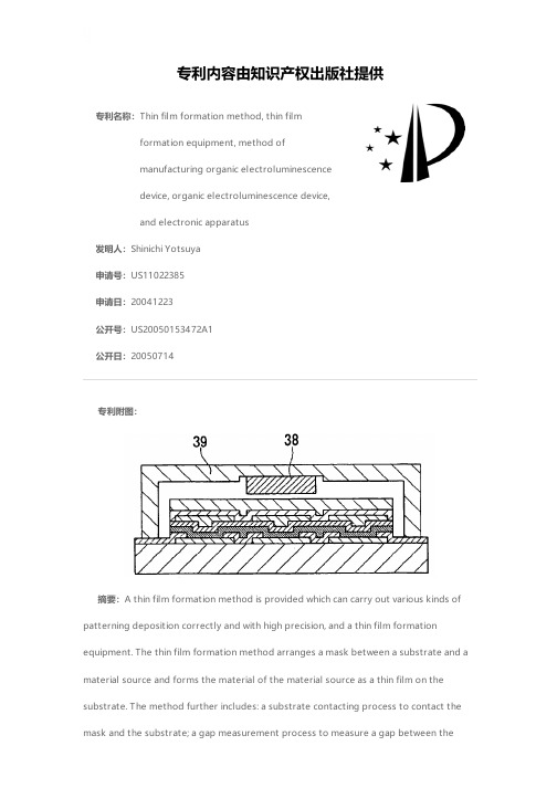
专利名称:Thin film formation method, thin film formation equipment, method of manufacturing organic electroluminescence device, organic electroluminescence device, and electronic apparatus
发明人:Shinichi Yotsuya 申请号:US11022385 申请日:2004 1223 公开号:US200501534 72A1 公开日:20050714
专利附图:
摘要:A thin film formation method is provided which can carry out various kinds of patterning deposition correctly and with high precision, and a thin film formation equipment. The thin film formation method arranges a mask between a substrate and a material source and forms the material of the material source as a thin film on the substrate. The method further includes: a substrate contacting process to contact the mask and the substrate; a gap measurement process to measure a gap between the
FORMATION OF THIN FILM
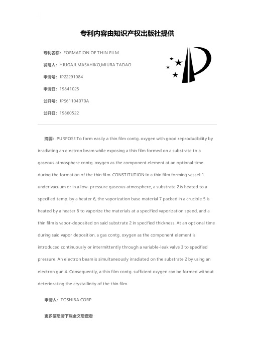
专利名称:FORMATION OF THIN FILM发明人:HIUGAJI MASAHIKO,MIURA TADAO 申请号:JP22291084申请日:19841025公开号:JPS61104070A公开日:19860522专利内容由知识产权出版社提供摘要:PURPOSE:To form easily a thin film contg. oxygen with good reproducibility by irradiating an electron beam while exposing a thin film formed on a substrate to a gaseous atmosphere contg. oxygen as the component element at an optional time during the formation of the thin film. CONSTITUTION:In a thin film forming vessel 1 under vacuum or in a low- pressure gaseous atmosphere, a substrate 2 is heated to a specified temp. by a heater 6, the vaporization base material 7 packed in a crucible 5 is heated by a heater 8 to vaporize the materials at a specified vaporization speed, and a thin film is vapor-deposited on said substrate 2 in specified thickness. At an optional time during said vapor deposition, a gas contg. oxygen as the component element is introduced continuously or intermittently through a variable-leak valve 3 to specified pressure. An electron beam is simultaneously irradiated on the substrate 2 by using an electron gun 4. Consequently, a thin film contg. sufficient oxygen can be formed without deteriorating the crystallinity of the thin film.申请人:TOSHIBA CORP更多信息请下载全文后查看。
FORMATION OF THIN FILM

专利名称:FORMATION OF THIN FILM发明人:MATSUSHIMA FUMIAKI,ONO YOSHIHIRO 申请号:JP25782188申请日:19881013公开号:JPH02104697A公开日:19900417专利内容由知识产权出版社提供摘要:PURPOSE:To form a film excellent in adhesion properties by performing a first-time film formation and thereafter heat treating the film and successively cleaning an electrode pattern sufficiently and there-after performing a second or more-times film formation in the case of performing film formation on a plurality of electrode patterns provided on the same base plate by micelle electrolysis at a plurality of times. CONSTITUTION:Organic or inorganic fine pigment powder insoluble or difficult to be dissolved in the aq. soln. described hereunder is incorporated in the aq. soln. contg. both a surfactant having the property charged to positive by electrolytic oxidation and a supporting electrolyte such as Li2SO4 and thereby a plurality of electrolytic aq. solns. are prepared. In the case of forming films on a plurality of electrode patterns provided on a base plate for film formation by micelle electrolysis at a plurality of times while utilizing the above-mentioned electrolytic aq. soln., a first time film is formed into a prescribed pattern and thereafter heat-treated and successively the electrode pattern to be film-formed in a second or more times is sufficiently cleaned and then ensuing film formation is performed in the prescribed patterns. The film excellent in adhesion properties on the base plate is formed by repeating this stage and performing film formation at a plurality of times.申请人:SEIKO EPSON CORP 更多信息请下载全文后查看。
Thin film formation device and semiconductor film
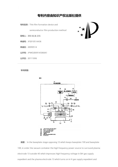
专利名称:Thin film formation device andsemiconductor film production method发明人:津田 睦,滝 正和申请号:JP2010514436申请日:20090514公开号:JPWO2009145068A1公开日:20111006专利内容由知识产权出版社提供专利附图:摘要: In the baseplate stage opposing 12 which keeps baseplate 100 and baseplate 100, in order the vacuum container the high frequency power source to surround plasma electrode 13 outside 40 which impresses high frequency voltage in SiH gas supply expedient and the plasma electrode 13 which turns on in H gas supply expedient andwhen forming a membrane at the time of 10 which possesses the plasma electrode 13 which is provided and membrane it supplies the H gas to vacuum container 10 with fixed flow/turn off the supply of the SiH gas to vacuum container 10 with opening and closing the gas valve 25, and vacuum container 10, the sealed box 20 which is grounded and the SiH gasIn order periodically to supply to vacuum container 10, as opening and closing the gas valve 25 is controlled, same period doing in opening and closing the gas valve, 25 the control section 60 which adds amplitude modulation to the high-frequency power which it impresses in plasma electrode 13 and, it has, gas valve 25 is arranged inside sealed box 20.申请人:三菱電機株式会社地址:東京都千代田区丸の内二丁目7番3号国籍:JP代理人:酒井 宏明更多信息请下载全文后查看。