PE83363中文资料
AEMC PowerPad III Model 8336产品说明书

Transient Capture on theAEMC PowerPad III Model 8336Transients are short-term current and voltage phenomena that occur in the system under measurement. The process the AEMC PowerPad III Model 8336 uses for recording transients is as follows:•The instrument sampling rate is a constant256 samples per cycle.•When a transient search is started on theinstrument, each sample is compared to thecorresponding sample from the precedingcycle.•The transient threshold is the user-definedamount of volts or amps for any datapoint todiffer from the corresponding datapointexactly 1 cycle earlier. The preceding cycledefines the mid-point of the trigger envelopeand is used as reference.•As soon as a sample is outside the envelope,the triggering event occurs; the transient datais then captured by the instrument.•The cycle preceding the event and the threefollowing cycles are saved to memory.The following explains how to configure, schedule,and view a transient recording session on the Model8336. These instructions assume you are using theModel 8336 as a standalone instrument.Note that you can also perform these tasks by connecting the instrument to a computer running AEMC’s DataView software. For more information, see the PowerPad III Model 8336 User Guide.Transient Recording Configuration1. With the instrument turned ON, press the button to display the Waveform Capturescreen.2. Ensure Transient is highlighted, then press .●If there are no transient detection sessions stored in the instrument, the DetectionSchedule screen appears.●If there are recordings in the instrument, the Detection List screen is displayed. In thiscase, press to display the Detection Schedule screen.3. Press the function button under the icon to display the Voltage Thresholdsscreen. At the top of the screen is the Threshold Set-up field. Options are:●4V: The same voltage difference threshold applies to all phases and the neutral in theelectrical hook-up●3V+VN: One threshold applies to the phases and one applies to neutral●V1+V2+V3+V4: Each phase and neutral has its own assigned thresholdDepending on the electrical hook-up currently under measurement, not all these options may be available.4. The setting in this field determines which of the four fields below it (1, 2, 3, and N) areeditable:●4V: a single field is active for 1, 2, 3, and N.●3V+VN: one field is active for 1, 2, and 3; and another is active for N.●V1+V2+V3+N: each field is active.To edit a voltage threshold field, highlight it using the up and down arrow buttons, thenconfirm the selection by pressing . Use the left and right arrows to select a digit, and the up and down arrows to change it. You can also use these buttons to select units (V or kV).Press to confirm the edited field.5. Press the A button to display the Current Thresholds screen. This is similar to the VoltageThreshold screen. You can select which thresholds apply to which phases, and specify the value of the threshold (1mA through 9999kA). As with the voltage thresholds, not all these options may apply to all electrical hook-up types.Note that current transients typically occur frequently. We recommend performing a current transient search only when looking for a specific type of transient. At other times, such as when you are primarily interested in voltage transients, you can effectively disable current transient searching by setting the threshold to its maximum value.Scheduling Transient Detection1. Press the button to display the Waveform Capture screen.2. Ensure Transient is highlighted, then press .●If there are no transient detection sessions stored in the instrument, the DetectionSchedule screen appears.●If there are recordings in the instrument, the Detection List screen is displayed. In thiscase, press the button to display the Detection Schedule screen.3. This screen displays four input fields:●Start defines the time and date when the recording starts. This must be later than thecurrent date and time.●Stop specifies when the recording ends. This must be later than the start date and time.●Transient Count defines the maximum number of transients that you want to capturebefore stopping the session.●Name allows you to name the test. This can be 8 characters long.4. Use the arrow and buttons to highlight, select, and edit these fields.5. Press the button to write the settings to the instrument and start the session.6. If not enough memory is available, an error message appears informing you of this.Otherwise, the transient detection session will begin at the scheduled start time and date.If a session is scheduled but not yet started, the message DETECTION ON STANDBY appears on the screen until the start time is reached, at which point the message changes to DETECTION IN PROGRESS.When the session is active, the icon blinks at the top of the screen, along with a status bar showing the progress of the session. In addition, the (stop) button appears in place of .During the session, the Transient Count number is reduced by 1 every time a transient is recorded. If this number counts down rapidly and appears as though it will reach zero well before stop time is reached, we recommend stopping the session and setting the threshold to a higher, less sensitive value. The session will continue until: (1) you press , (2) the Transient Count limit is reached (see Step 3), or (3) the stop time/date is reached.7. When the transient detection session is finished, it appears in the Detection List screen. Youcan now open the session and view its contents, as explained in the following.Viewing a Transient Detection Session1. At the Detection Schedule screen, press the button.For all other displayed screens, press the button, and then select Transient.Either action displays the Detection List screen.2. If more than one transient detection recording is stored, use the arrows to select thedesired recording, then press to open it.In the preceding illustration:1 Location in the record of the zonedisplayed.4 Move cursor to transient triggering time.2 Instantaneous value of the signalsaccording to the position of the cursor on the scale. Use ◄ and ► to move cursor.5 Number assigned to displayed graph (e.g.1 is highlighted indicating channel V1 triggered capture of the transient)3 Move cursor to one period of the signalbefore transient triggering time. 6 Zoom In/Out。
8336-bom
CONN-ML-242P(1473463-1)-AMP PJ1196012A0042801CONN-FM-4P(175487-4)-AMP PJ88006012A0044501CONN-ML-150P(1565696-1)-AMP PCMCIA6017A0015801CABLE-TC8245-DC PW CORD DC-IN CABLE6017A0017101CABLE-TC8245-MODEM HARNESS-RJ11MODEM CABLE6019A01083T1CPU-NORTHWOOD-1.8GHZ-512K-MPGA-ITL(478PI CPU6026A0011601SWCH-SKELAKA010-ALPS S1036053A0063901THERMAL-TC8326-01(801PBM05)FAN6035A0001301FFC-SML2CD-50x62-BDx6(BL)-P0.5-S4-N-M-K(FPC26035A0001401FFC-(SML2CD-30x125-BDx6(BL)-P0.5-S4-N-M-FPC16053A0051501BRACKET-TC8245-IO-016054A0031901INSU-TC8245-CARDBUS-02-UP(PET)6053A0051401BRACKET-TC8245-HEAT SINK-026051A0040901DOOR-TC8245-DOCKING-01(AMP 1473477)6054A0031601INSU-TC8245-DOCKING CONN-01(MYLAR)6052A0010601SCREW-I20100M-NI-NYLOK6054A0031701INSU-TC8245-MEMORY-02(PC)SCREW-B20060M-MC6054A0032001INSU-TC8245-CPU PS2-01(PET)6052A0007901NUT-TC8245-M2.0x5.0Dx6.0T-M2.5x4.0L6052A0008201SCREW-B20040M-BNI-MC6052A0008401SCREW-B20080M-MC60520D056602SCREW-SKT475115M(+WASHER)605302281102STPN-P6403A-D-SUB-SCREW6052A0006601SCREW-I20040M(3.5Dx0.4T)-NYLOK6054A0037801RBHD-TC8326-M/B-01(20X4.5X4.0T)6054A0037501DSTP-TC8245-PCB-01(G9000,13x13)111MBB9500A0SA-M/B-SMD-TC83076060A0083501LABEL.BLANK-TC8243-01-47x256060A0083701LABEL.BLANK-TC8243-01-40x236053A0062901HEAT SINK-TC8326-NORTH BRIDGE-01(AL)6054A0040901RBHD-TC8326-M/B-01(8.0X3.5X2.4T)6054A0040801INSU-TC8326-NORTH BRIDGE-02(PC)6052A0009901SCREW-I25040M(4.5Dx1.0T)-BNI-NYLO6054A0042001FOAM-TC8326-FAN-01(UEI)6054A0042401DSTP-TC8326-CARDBUS-01(G9000 5x25L)6054A0042301GASKET-TC8326-FPC CABLE-01(15x0.1x35L) 605406334101GREASE-G750-THERMAL6054A0066901PAD-ELASTOMER-20.0x4.0x3.3MM-RUBBER-BLACPAD-ELASTOMER-25.0x6.0x5.4MM-RUBBER-BLAC111MBB9500A06010071012ATCAP-CHIP-101-J,50V-0402-TAP C446C90506010071020ATCAP-CHIP-102-K,50V-X7R-TAP(0402)C372C371C366C36460100710220ZCAP-CHIP-102-J,50V-NPO-TAP(0603)C902360100710300ZCAP-CHIP-103-K,50V-TAP(0603)-X7R C429C408C407C246C195C118C1176010071031BTCAP-CHIP-103-K,16V-X7R-0402-TAP C9157C13960100710402TCAP-CHIP-104-K,X7R-16V-TAP(0603)C8813C8825C8911C8948C8772C653C37C36C297C9201C9159C9101C9072C9022C9004C9002C8949C294C209C208C207C206C205C133C132C121C268C267C264C263C214C210C211C212C213C915160100710430YCAP-CHIP-104-Z,Y5V-50V-TAP(0805)C9C976C977C2C735C73660100710431ZCAP-CHIP-104-Z,25V(Y5V)-TAP(0603)C53C529C528C527C530C531C532C533C534C524C513 C514 C515 C516 C518 C519 C52 C523 C535 C552 C557 C56 C560 C565 C566 C567 C568 C569 C547 C536 C537 C539 C54 C541 C542 C543 C544 C546 C303 C304 C31 C32 C33 C34 C35 C365 C367 C301 C284 C285 C287 C288 C289C30 C300 C370 C449 C450 C451 C456 C487 C49 C51 C511 C447 C373 C378 C38 C381 C39 C40 C401 C427 C570 C634 C635 C636 C637 C638 C639 C640 C641 C642 C633 C624 C625 C626 C627 C628 C629 C630 C631 C632 C643 C68 C7C732 C733 C734 C8C9030 C975 C67 C644 C645 C646 C647 C648 C649 C65 C654 C66 C585 C586 C587 C588 C589 C590 C591 C593 C594 C583 C572 C573 C575 C577 C578 C579 C58 C581 C582 C596 C61 C610 C611 C612 C614 C618 C62C622 C609 C597 C598 C599 C600 C601 C603 C604 C605 C606 C1131 C1134 C1140 C116 C1186 C1187 C1188 C1189 C1192 C1130 C108 C109 C11 C1121 C1122 C1123 C1124 C1125 C1128 C1193 C1221 C1222 C1225 C1226 C1229 C1230 C1237 C1238 C1239 C1220 C1195 C1198C1201 C1205 C1211 C1216 C1217 C1218 C1011 C1012 C1013 C1014 C1015 C1016 C1017 C1018 C1019 C1010 C1001 C1002 C1003 C1004 C1005 C1006 C1007 C1008 C1009 C1020 C104 C1043 C1044 C1049 C1050 C1055 C1056 C106 C107 C1038 C1021 C1022 C1023 C1024 C1025 C1026 C1031C1037 C1241 C187 C188 C189 C193 C21 C22 C23 C230 C232 C186 C175 C176 C177 C178 C180 C182 C183 C184 C185 C234 C269 C27 C270 C279 C28 C280 C281 C282 C283 C262 C235 C236 C237 C24 C247 C25 C26 C260 C261 C1258 C1262C146C147C148C149C15C150C1255C1242C1243C1245C1246C1247C1249C1250C1251C1254C151C164C165C166C167C168C171C172C173C174C162C152C153C154C155C156C16C159C158C157C129C13060100710603TCAP-CHIP-106-K,6.3V-X5R-TAP(1206)C526C563C86C88C525C228C229C517C520C521C95C96C97C98C99C94C89C90C91C92C93C113C114C115C17C18C112C102C103C105C110C111C223C224C225C226C227C222C19C190C191C192C206010072202ATCAP-CHIP-220-J,50V-TAP(0402)C51016010072240CTCAP-CHIP-224-K,10V-X7R-TAP(0603)C900360100733302TCAP-CHIP-333-K,16V-X7R-0603-TAP C87716010074702ATCAP-CHIP-470-J,50V-TAP(0402)C90006010074750CTCAP-CHIP-475-K,10V-X7R-1206-TAP C9005C9054C9103C9153C9203C8913C119C233C276C277C646010A0009801CAP-CHIP-271-J,50V-X7R-0402-TAP C9051C51006010A0010601CAP-CHIP-221-J,25V-NPO-0402-TAP C81C78C77C76C448C4526010A0010701CAP-CHIP-222-J,50V-X7R-0402-TAP C9055C9006C6526010A0014801CAP-CHIP-101-K,3000V-NPO-1808-TAP C293 6010A0024101CAP-METAL-227-2V-AP-Dx3-ESR18M-TAP-MAT C9062C9063C9064C9065C9013C9014C9015C90166010A0024501CAP-CHIP-106-K,16V-X5R-1210-TAP C9205C9155C9105C89156010A0024801CAP-CHIP-391-K,50V-X7R-0402-TAP C51106010A0025001CAP-CHIP-474-K,16V-X7R-0805-TAP C8946C89476010A0025101CAP-CHIP-471-K,50V-X7R-0402-TAP C9024C505C4776010A0025301CAP-CHIP-104-K,10V-X5R-0402-TAP C6506010A0025701CAP-CHIP-332-K,50V-X7R-0402-TAP C606010A0026101CAP-CHIP-105-K,6.3V-X7R-0603-TAP C9052C9001C8912C8910C8773C8770C75C74C5114C9202C9152C9150C9102C9100C9099C9098C9097C5113C218C217C216C215C194C163C160C141C137C305C29C278C257C256C219C220C221C2316010A0026201CAP-CHIP-105-K,16V-X5R-0805-TAP C8812C8803C250C2496010A0026301CAP-CHIP-106-K,10V-X5R-1210-TAP C336C298C1016010A0026401CAP-CHIP-226-K,6.3V-X5R-1210-TAP C545C461C434C551C79C80C142C143C144C145C432C170C169C1206010A0028701CAP-METAL-337-4V(TEPSLDOJ337M(25)12R)-TA C562C6236010A0029001CAP-CHIP-225-K,10V-X5R-0805-TAP C1386010A0029101CAP-CHIP-475-K,X5R-6.3V-0805-TAP C90256010A0029201CAP-CHIP-152-J,X7R-50V-0805-TAP C90296010A0029301CAP-CHIP-472-K,X7R-50V-0402-TAP C9071C90706010A0030001CAP-AL-226-20V(20SVP22M)-TAP-SANYO C9068C9067C9020C90196010A0030101CAP-METAL-107-4V(TEPSLB20G107M(45)8R)-TA C9156C9206C9916C9109C615C9158C5226010A0030301CAP-AL-4.7UF-10V(MF10FC4R7MA6)-TAP C2866011A0010401DIODE-1SS294-TE85R-TSB(3PIN)D8907D9000D9050D9100D9150D9200D108D112D126D8860D8825D50026011A0010501DIODE-RD6.2Z-T2B-TAP-NEC D5003D50D121D120D5004D51D52D53D119D110D111D113D114D118D117D116D1156011A0011001DIODE-SCH-EA60QC03L-TE16F2-TAP-NIR(3PIN)D8003D8800D8802D88056011A0011101DIODE-SCH-EC31QS03L-TAP-NI(2PIN)D9052D9051D9002D900160120IA12610CONN-FM-150P(1123215-1)-AMP PJ3660120IA15470CONN-ML-2P(SM02B-SRSS-TB)-JST PJ1266012A0040701CONN-FM-6P(440021-3)-AMP PJ536012A0040801CONN-FM-30P(52559-3092)-MLX PJ3026012A0040901CONN-FM-50P(FH12-50S-0.5SV)-HRS PJ3656012A0041001CONN-ML-70P(DJ33-070FL-HN-3)-KEL PJ1166012A0041401CONN-ML-44P(KKS-RSR44-43TB)-DDK PJ5206012A0041501CONN-ML-8P(UB91123-ST1-HT)-FOX PJ526012A0042201CONN-FM-124P(440360-1)-AMP PJ1186012A0042301CONN-FM-15P(1-440135-2)-AMP PJ50026012A0050801CONN-FM-15P(7753S-15G2T-HC)-SUYIN PJ50026012A0042401CONN-FM-25P(1-440136-1)-AMP PJ1216012A0050701CONN-FM-25P(7754S-25G2T-AA)-SUYIN PJ121 6012A0042501CONN-ML-9P(1-1470269-1)-AMP PJ1206012A0066101CONN-ML-9P(7756P-09G2-AA)-SUYIN PJ1206012A0042601CONN-FM-(2-440366-7)-RJ11/RJ45-AMP PJ1246012A0042901CONN-ML-15P(DF3A-15P-2DSA)-HRS PJ8506012A0043001CONN-ML-14P(DF3A-14P-2DSA)-HRS PJ8516012A0043101CONN-FM-80P(C-1565104)-AMP PJ8526012A0043201CONN-ML-3P(BM03B-SRSS)-JST PJ87706012A0043601CONN-ML-30P(3-179397-5)-AMP PJ1256012A0043701CONN-ML-2P(440371-2)-AMP PJ3116012A0043801CONN-ML-2P(440371-3)-AMP PJ3106012A0051601CONN-FM-200P(3-1565779-5)-AMP PJ1006012A0052401CONN-FM-479P(1565228-1)-TAP-AMP IS360130B0000ZTRES-CHIP-0-5%-1/16W-0402-TAP W9003W9002W9001W9W8910W5043W9005W9203W9202W9152W9102W9060W9007W119W1125W1123W1120R9110R9025R9024W143W5W39W38W37W162W21W36W920660130B10000XRES-CHIP-10-5%-1/16W-0402-TAP R426R5077R5078R5081R5082R158R159R163R363R4086013A0072501RES-CHIP-100-5%-1/3W-1210-TAP R885360130B1002BZRES-CHIP-10K-0.5%-1/16W-0402-TAP R9028R8776R231R230 60130B1010ZTRES-CHIP-100-5%-1/16W-0402-TAP R9169R9158R29260130B1020ZTRES-CHIP-1K-5%-1/16W-0402-TAP R9101R9054R9004R8939R435R95R94R9201R9168R9151R357R356R26R218R410R380R379R378R35960130B10300ZRES-CHIP-10K-5%-1/10W-0603-TAP R4560130B1030ZTRES-CHIP-10K-5%-1/16W-0402-TAP R355R333R299R253R252R247R234R371R9171R65R6R409R388R375R372R226R181R178R177R16R108R1R182R221R213R210R207R205R192R185R20360130B1040ZTRES-CHIP-100K-5%-1/16W-0402-TAP R436R20460130B10609TRES-CHIP-10M-5%-1/10W-0603-TAP R17660130B15100YRES-CHIP-150-5%-1/16W-0402-TAP R34560130B2020ZTRES-CHIP-2K-5%-1/16W-0402-TAP R19760130B2200ZTRES-CHIP-22-5%-1/16W-0402-TAP R78R79R80R81R82R77R317R420R74R75R76 60130B2210ZTRES-CHIP-220-5%-1/16W-0402-TAP R9163R9109R9164R9165R9167R9208R312R324R325R327R9021R8946R33460130B22300YRES-CHIP-22K-5%-1/16W-0402-TAP R266R268R902760130B30500TRES-CHIP-3M-5%-1/10W-0603-TAP R18460130B3300ZTRES-CHIP-33-5%-1/16W-0402-TAP R390R235R209R174R175R18860130B3310ZTRES-CHIP-330-5%-1/16W-0402-TAP R464R463R441R440R439R433R43260130B33300TRES-CHIP-33K-5%-1/16W-0402-TAP R89836013A0072401RES-CHIP-47-5%-1/3W-1210-TAP R32360130B4710ZTRES-CHIP-470-5%-1/16W-0402-TAP R8875R72R71R455R438R9166R8994R8993R8898R8897R332R330R329R272R270R437R352R350R347R33560130B4720ZTRES-CHIP-4.7K-5%-1/16W-0402-TAP R8877R9099R9156R8818R144R145R507960130B4730ZTRES-CHIP-47K-5%-1/16W-0402-TAP R358R367R12R434R8813R8823R8996R100R117R232R233R311R306R23660130B5100ZTRES-CHIP-51-5%-1/16W-0402-TAP R316R309R308R301R302R30760130B5600ZTRES-CHIP-56-5%-1/16W-0402-TAP R87R86R85R84R88R89R9R90R91R132R14R3R460R461R83R68R67R46260130B56100YRES-CHIP-560-5%-1/16W-0402-TAP R917060130BA0003TRES-CHIP-0-5%-1/8W-0805-TAP W9051W900460130BA1033TRES-CHIP-10K-5%-1/8W-0805-TAP R879560130BA1043SRES-CHIP-100K-5%-1/10W-0805-TAP R882060130BA2203TRES-CHIP-22-5%-1/8W-0805-TAP R9204R9154R9104R9053R9002R894260130BA4713TRES-CHIP-470-5%-1/8W-0805-TAP R10360130CJ0019TRES-AR-8P4R-0-5%-1/16W-2010-TAP RM906060130CJ0022TRES-AR-8P4R-1K-5%-1/16W-2010-TAP RM217RM216RM120RM119RM118RM11760130CJ0026TRES-AR-8P4R-10-5%-1/16W-2010-TAP RM30RM29RM28RM2760130CJ0028TRES-AR-8P4R-47K-5%-1/16W-2010-TAP RM115RM116RM19RM58RM100RM101RM109RM113RM11460130CJ0111TRES-AR-8P4R-10K-5%-1/16W-2010-TAP RM210RM212RM215RM5011RM200RM201RM202RM204RM206RM20760130CJ0112TRES-AR-8P4R-33-5%-1/16W-2010-TAP RM112RM111RM11060130CJ0115TRES-AR-8P4R-22-5%-1/16W-2010-TAP RM5RM26RM25RM24RM6RM7RM8RM9RM23RM10RM11RM12RM13RM14RM21RM20RM16RM156013A0001301RES-AR-8P4R-56-5%-1/16W-2010-TAP RM47RM48RM49RM46RM45RM44RM55RM54RM53RM51RM50RM43RM35RM34RM33RM32RM3RM1RM36RM42RM41RM40RM39RM38RM376013A0003101RES-CHIP-1.5K-5%-1/16W-0402-TAP R1306013A0003401RES-CHIP-300-5%-1/16W-0402-TAP R73R55R2736013A0006501RES-CHIP-1-5%-1/10W-0603-TAP R9200R9150R9100R88106013A0014601RES-CHIP-75-1%-1/8W-0805-TAP R8R429R428R4276013A0015401RES-CHIP-24-5%-1/2W-2010-TAP R88746013A0049201RES-METAL-0.02-1%-1W-2512-TAP R9209R91556013A0049601RES-CHIP-2.2k-5%-1/16W-0402-TAP R8997R8824R50806013A0049801RES-CHIP-470-5%-1/3W-1210-TAP R8801R8802R8803R8800R8799R8798R8797R87966013A0050401RES-AR-4P2R-2.2K-5%-1/16W-2010-TAP RM221RM2206013A0050701RES-CHIP-20K-5%-1/16W-0402-TAP R90506013A0050801RES-CHIP-8.2K-5%-1/16W-0402-TAP R70R211R2156013A0051101RES-CHIP-68K-5%-1/16W-0402-TAP R267R2656013A0051201RES-CHIP-200-5%-1/16W-0402-TAP R61R62R63R64R56R57R58R59R606013A0051901RES-CHIP-100-0.5%-1/16W-0402-TAP R54R52R425R2196013A0052101RES-CHIP-120-0.5%-1/16W-0402-TAP R4246013A0052301RES-CHIP-150-0.5%-1/16W-0402-TAP R9015R224R2226013A0052501RES-CHIP-200-0.5%-1/16W-0402-TAP R92066013A0052601RES-CHIP-220-0.5%-1/16W-0402-TAP R5085R5084R50836013A0052801RES-CHIP-300-0.5%-1/16W-0402-TAP R9107R156R1556013A0053201RES-CHIP-1K-0.5%-1/16W-0402-TAP R9019R9020R9159R248R249R8770R87746013A0053601RES-CHIP-2K-0.5%-1/16W-0402-TAP R7R4R26013A0053701RES-CHIP-2.2K-0.5%-1/16W-0402-TAP R9205R9161R9160R90296013A0053801RES-CHIP-4.7K-0.5%-1/16W-0402-TAP R9207R9108R8945R8773R448R4446013A0053901RES-CHIP-6.8K-0.5%-1/16W-0402-TAP R9106R87716013A0054101RES-CHIP-11K-0.5%-1/16W-0402-TAP R87756013A0054201RES-CHIP-15K-0.5%-1/16W-0402-TAP R90086013A0054401RES-CHIP-18K-0.5%-1/16W-0402-TAP R90266013A0054501RES-CHIP-20K-0.5%-1/16W-0402-TAP R9202R9152R91026013A0054601RES-CHIP-22K-0.5%-1/16W-0402-TAP R87726013A0054901RES-CHIP-47K-0.5%-1/16W-0402-TAP R8941R450R4496013A0055001RES-CHIP-51K-0.5%-1/16W-0402-TAP R90526013A0055301RES-CHIP-68K-0.5%-1/16W-0402-TAP R8940 6013A0055401RES-CHIP-100K-0.5%-1/16W-0402-TAP R9203R9153R9103R447R446R269R9006.6013A0055501RES-CHIP-56-0.5%-1/16W-0402-TAP R2286013A0056001RES-AR-8P4R-150-5%-1/16W-2010-TAP RM2186013A0056201RES-AR-4P2R-220-5%-1/16W-2010-TAP RM9051RM9050RM18RM176013A0056301RES-CHIP-560-0.5%-1/16W-0402-TAP R4236013A0056701RES-AR-4P2R-4.7K-5%-1/16W-2010-TAP RM209RM2086013A0056901RES-AR-4P2R-10K-5%-1/16W-2010-TAP RM31RM302RM301RM300RM22RM219RM205RM1086013A0057001RES-AR-4P2R-47K-5%-1/16W-2010-TAP RM576013A0058301RES-AR-8P4R-100-5%-1/16W-2010-TAP RM211 6013A0058701RES-AR-8P4R-8.2K-5%-1/16W-2010-TAP RM46013A0069301RES-CHIP-36.5-0.5%-1/16W-0402-TAP R246R1526013A0069401RES-CHIP-18.2-0.5%-1/16W-0402-TAP R1536013A0069501RES-CHIP-8.2K-0.5%-1/16W-0402-TAP R1736013A0069601RES-CHIP-475-0.5%-1/16W-0402-TAP R966013A0069701RES-CHIP-3.6K-0.5%-1/16W-0402-TAP R89436013A0069801RES-CHIP-910K-0.5%-1/16W-0402-TAP R1806013A0074301RES-CHIP-160-0.5%-1/16W-0402-TAP R89446013A0070001RES-CHIP-82-0.5%-1/16W-0402-TAP R264R2636013A0070101RES-CHIP-27.4-0.5%-1/16W-0402-TAP R3446013A0070301RES-CHIP-62K-1%-1/16W-0402-TAP R4216013A0070501RES-CHIP-3.9K-0.5%-1/16W-0402-TAP R90106013A0070701RES-CHIP-5.1K-0.5%-1/16W-0402-TAP R9023R90146013A0070801RES-CHIP-750-0.5%-1/16W-0402-TAP R90226013A0070901RES-CHIP-301-0.5%-1/16W-0402-TAP R262R250R223R2206013A0071001RES-CHIP-40.2-0.5%-1/16W-0402-TAP R2436013A0071101RES-CHIP-24.9-0.5%-1/16W-0402-TAP R244R2456013A0071201RES-CHIP-30K-0.5%-1/16W-0402-TAP R90316013A0071301RES-CHIP-39-0.5%-1/16W-0402-TAP R3466013A0071401RES-CHIP-110K-0.5%-1/16W-0402-TAP R90616013A0071501RES-CHIP-33-0.5%-1/16W-0402-TAP R286R285R284R287R97R98R99R282R102R106R275R276R278R279R2806013A0071601RES-CHIP-75k-0.5%-1/16w-0402-TAP R90006013A0071701RES-CHIP-3.6K-5%-1/16W-0402-TAP R91576013A0071801RES-CHIP-620-0.5%-1/16W-0402-TAP R4226013A0071901RES-CHIP-51.1-0.5%-1/16W-0402-TAP R69R66R50R496013A0072001RES-CHIP-680K-5%-1/16w-0402-TAP R9007R90036013A0072101RES-CHIP-1.8K-5%-1/16W-0402-TAP R90116013A0072201RES-CHIP-49.9-0.5%-1/16W-0402-TAP R227R51R53R225R216R116R1076013A0072301RES-CHIP-30.1-0.5%-1/16W-0402-TAP R2376013A0072701RES-AR-4P2R-1K-5%-1/16W-2010-TAP RM566013A0073601RES-METAL-0.002-1%-1W-2512-TAP R9017R905560140EA0241TCOIL-ACM0908-801-2P-TAP-TDK FL880060140EA0308TCOIL-BEAD-BK1608HS241-TAP-TAIYO FL116FL117 6014A0011201COIL-NLC322522T-330K-TAP-TDK L1106014A0011501COIL-NFM51R20P207-MURATA FL5016FL5015FL50146014A0012201IDUT-PLFC0735P-3R3B-3.3UH-TAP-TOKIN L9201L9151L9101L89086014A0012501IDUT-FBMJ3216HS800-T-TAP-TYD L9051L9100L9150L9200FL8907L9000L9001L90506014A0012901COIL-NL453232T-4R7J-4.7UH-TDK L4L3L2L16014A0014001COIL-FBMH1608HW471MT-TAIYO FL52FL51FL5FL53FL54FL6FL7FL125FL118FL119FL120FL121FL124FL123FL1226014A0014301COIL-MLF2012A1R8KT-TDK L5100L50136014A0014401COIL-CPI-1050-1R0-TAP-TOKIN L9052L90026015A0044101TRAN-FET-TPC8103-SO-TAP-TSB(8PIN)Q8805Q8770Q113Q1036015A0044201TRAN-FET-TPC8007-H-SO-TAP-TSB(8PIN)Q9152Q8862Q8861Q88606015A0044501TRAN-FET-2SK2159-TAP-NEC Q88676015A0044801TRAN-FET-UPA1760G-E2-TAP-NEC Q9200Q9150Q89106015A0045901TRAN-FET-UPA2750GR-E2-TAP-NEC Q91006015A0046001TRAN-2SC3392AY5-CP-TAP-SANYO(3PIN)Q14Q15Q2Q9Q9007Q1Q10Q11Q12Q136015A0046301TRAN-FET-UPA2700TP-E2-POWER HSOP8-TAP-NE Q9053Q9052Q9003Q90026015A0046401TRAN-FET-UPA2702TP-E2-POWER HSOP8-TAP-NE Q9051Q9050Q9001Q90006015A0046601TRAN-FET-UPA1770G-E2-POWER SOP8-TAP-NEC Q88086015A0046701TRAN-FET-SSM3K17FU-SC70-TAP-TSB(3PIN)Q8871Q8911Q8923Q8924Q8870Q8809Q8807Q8806Q9201Q9158Q9156Q9155Q9153Q9101Q9006Q8925Q125Q123Q122Q119Q118Q106Q101Q100Q19Q17Q16Q126Q127Q128Q1296018A0006501X'TAL-14.31818MHZ(FA-365)-EPS X16018A0006901X'TAL-8MHZ(CSTCE8M00G55-R0)-15PF-MURATA X1016018A0007201X'TAL-OSL-32.768KHZ(SG-3030JC)-EPS X1006018A0007901X'TAL-25MHZ(K30-3C0-SE)-50PPM-KYO X1046018A0008001X'TAL-14.3182MHZ(K30-3C0-E)-100PPM-KYO X10260190H3905TTIC-SN74CBTD3306-TSSOP-TAP-TI(8PIN)IC500460190H4172STIC-TC7SH08FU-SSOP-TAP-TSB(5PIN)IC9003IC8IC128IC126IC10060190H4400STIC-TC7SH04FU-SSOP-TAP-TSB(5PIN)IC139IC138IC12460190H4701STIC-MAX3243CAI-SSOP-TAP-MAX(28PIN)IC13060190HF0076SIC-LM358A-SOP-NS(8PIN)IC9151IC87706019A00200T2IC-ICH3-M-B1-BGA-ITL(421PIN)IC1036019A0023601IC-MAX1718EEI-QSOP-TAP-MAX(28PIN)IC90006019A0115401IC-MAX1718AEEI-QSOP-TAP-MAX(28PIN)IC90006019A0024201IC-MAX4524CUB-UMAX-TAP-MAX(10PIN)IC90016019A00615T1IC-BROOKDALE-M-FC-BGA-VER.A-ITL(593PIN)IC146013A0070201RES-CHIP-120K-0.5%-1/16W-0402-TAP R90016013A0070401RES-CHIP-13K-0.5%-1/16W-0402-TAP R90056019A0084101IC-MIC2563A-0BSM-SSOP-TAP-MICREL(28PIN)IC1186019A0087501IC-LMV822MMX-MSOP-NS(8PIN)IC1406019A0088101IC-TC7SH00FU-SSOP-TAP-TSB(5PIN)IC1046019A0088201IC-ADM1032AR-SO-8-TAP-A&D(8PIN)IC16019A0088401IC-TC7SH14FU-SSOP-TAP-TSB(5PIN)IC1546019A0088701IC-TC7SH32FU-SSOP-TAP-TSB(5PIN)IC127IC1660190H3429STIC-SI4920DY-SO8-TAP-SIL(8PIN)Q9159Q8863Q124 6019A0089101IC-T7L58XB-0101-YEBISU3S-BGA-TSB(328PIN)IC1126019A0089901IC-HD74LS125AFP-SOP-TAP-HTC(14PIN)IC50056019A0090301IC-LPC47N227-STQFP-SMSC(100PIN)IC1296019A0091801IC-MAX1714BEEE-QSOP-TAP-MAX(16PIN)IC9200IC9150IC9100IC89056019A0092301IC-93LC46BXT-I/SN-SOP-TAP-MCT(8PIN)IC1366019A0101301IC-NC7ST04P5X-SC70-TAP-FAIR(5PIN)IC108IC1016019A0102501IC-SN74AHCT1G04DCKR-SC70-TAP-TI(5PIN)IC108IC10160190H2155STIC-TC7W66FU(TE12L)-SSOP-TAP-TSB(8PIN)IC1536019A0102701IC-TC7WH14FU(TE12L)-SSOP-TAP-TSB(8PIN)IC196019A0102901IC-M306K7F8LRP-QFP-MTS(144PIN)IC1256019A0103201IC-MAX1897EGP-QFN-TAP-MAX(20PIN)IC90506019A0103501IC-MAX1922ESA.C71073-SO8-MAX(8PIN)IC1026019A0103601IC-DA82562ET-SSOP-ITL(48PIN)IC135 6019A0103701IC-E82802AB8-TSOP-ITL(40PIN)IC36019A0103801IC-ADP3342JRM-REEL7-MSOP-A&D(8PIN)IC90996026A0009101JACK-2PJ-002Y4104-SINGA PJ50016026A0010601SOKT-DDR-200P(1473005-1)-AMP PJ176026A0010701SOKT-DDR-200P(1473006-1)-AMP PJ166036A0003401FUSE-CERAMIC-8A-125V-SMD-6.1x2.69-TAP F88006036A0002801FUSE-3.15A-125V-4513.15-MLX F88016036A0002901FUSE-(451.010)-10A/125V-TAP-LITTELFUSE F88206050A0020701PCB-TC8325MB-40-8L-VER120-213x322-1.2T-W6050A0020801PCB-TC8325MB-40-8L-VER120-213x322-1.2T-C6026A0011201SWCH-SPPW810201-ALPS(4PIN)S1046013A0073901RES-CHIP-300K-0.5%-1/16W-0402-TAP R903260120IA18560CONN-ML-4P(BM04B-SRSS-TBT)-JST PJ1276019A0105201IC-ICS950811AG-TSSOP-ICS(56PIN)IC96019A0088001IC-MAX6501UKP-T-SOT23-TAP-MAX(5PIN)IC26052A0008501NUT-TC8245-MODEM-016014A0014201COIL-FBMH1608HW470MT-TAIYO FL5017FL50186016A0002101XMER-H1195T-TAP-PULSE T1006013A0009301RES-CHIP-33-1%-1/10W-0603-TAP R466011A0010901DIODE-SCH-EP10QY03-TAP-NI(2PIN)D8908D9101D9151D92016015A0046501TRAN-MMBT3904LT1-SOT23-TAP-ONSEMI Q91576052A0012101NUT-TC8326-VGA/B-01(7.5T)6014A0003801COIL-DLW21SN121SQ2L-TAP-MURATA FLW301FLW302FLW303FLW3046052A0011401NUT-TC8326-VGA/B-01(8.0T)6054A0066201SOLDER-BH63J8153C-ENTEK-ISHIKAWA。
BD6383EFV中文资料

Please contact our sales offices for details ;
U.S.A / San Diego Atlanta Dallas Germany / Dusseldorf TEL : +1(858)625-3630 TEL : +1(770)754-5972 TEL : +1(972)312-8818 TEL : +49(2154)9210 FAX : +1(858)625-3670 FAX : +1(770)754-0691 FAX : +1(972)312-0330 FAX : +49(2154)921400 FAX : +44(1)908-282-528
Appendix1-Rev1.1
Contact us
Attached-1
Thank you for your accessing to ROHM product informations. More detail product informations and catalogs are available, please contact your nearest sales office.
(Contact address for overseas customers in Japan)
Yokohama
As of 18th. April 2005
United Kingdom / London TEL : +44(1)908-282-666 France / Paris China / Hong Kong Shanghai Dilian Beijing Taiwan / Taipei Korea / Seoul Singapore Malaysia / Kuala Lumpur Philippines / Manila Thailand / Bangkok
593066-3中文资料
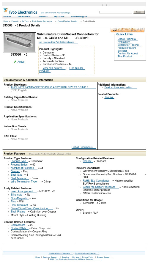
593066-3 Product DetailsHome | Customer Support | Suppliers | Site Map | Privacy Policy | Browser Support© 2008 Tyco Electronics Corporation All Rights Reserved SearchProducts Documentation Resources My Account Customer SupportHome > Products > By Type > Pin & Socket Connectors > Product Feature Selector > Product Details593066-3Active Subminiature D Pin/Socket Connectors forMIL-C-24308 and MIL-C-39029Not reviewed for RoHS ComplianceProduct Highlights:?Connector?Product Series = 90?Density = Standard?Terminate To Wire?Number of Positions = 44View all Features | Find SimilarProductsCheck Pricing &AvailabilitySearch for ToolingProduct FeatureSelectorContact Us AboutThis ProductQuick LinksDocumentation & Additional InformationProduct Drawings:?AMPLIMITE NONMAGNETIC PLUG ASSY WITH SIZE 22 CRIMP P...(PDF, English)Catalog Pages/Data Sheets:?None AvailableProduct Specifications:?None AvailableApplication Specifications:?None AvailableInstruction Sheets:?None AvailableCAD Files:?None AvailableList all Documents Additional Information:?Product Line InformationRelated Products:?ToolingProduct Features (Please use the Product Drawing for all design activity)Product Type Features:?Product Type = Connector?Product Series = 90?Number of Positions = 44?Gender = Plug?Shell Size = 3?Shell Material = Brass?Wire Termination Type = CrimpBody Related Features:?Insert Arrangement = MS18275-2?Blindmate = No?Non-Magnetic = Yes?Pins = With?Rear Grommet = No?Power/Signal/Coax Combination = No?Shell Plating = Cadmium over Copper?Mount Style = Floating BushingContact Related Features:?Contact Size = 22?Contact Style = Crimp Snap-in?Contact Material = Copper Alloy?Contact Mating Area Plating Material = Goldover Nickel Configuration Related Features:?Density = StandardIndustry Standards:?Government/Industry Qualification = Yes?Government/Industry Part Number = M24308/8-309F?RoHS/ELV Compliance = Not reviewed forELV/RoHS compliance?Lead Free Solder Processes = Not reviewed forlead free solder process?NASA Qualification = NoConditions for Usage:?Terminate To = WireOther:?Brand = AMPProvide Website Feedback | Contact Customer Support。
MGA83563资料
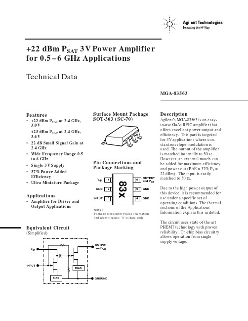
+22 dBm P SAT 3V Power Amplifier for 0.5–6 GHz Applications Technical DataMGA-83563Features•+22 dBm P SAT at 2.4 GHz,3.0V +23 dBm P SAT at 2.4 GHz,3.6V•22 dB Small Signal Gain at 2.4 GHz •Wide Frequency Range 0.5to 6 GHz •Single 3V Supply •37% Power Added Efficiency •Ultra Miniature PackageApplications•Amplifier for Driver and Output ApplicationsSurface Mount Package SOT-363 (SC-70)Pin Connections and Package MarkingEquivalent Circuit(Simplified)Note:Package marking provides orientation and identification; “x” is date code.DescriptionAgilent’s MGA-83563 is an easy-to-use GaAs RFIC amplifier that offers excellent power output and efficiency. This part is targeted for 3V applications where con-stant-envelope modulation is used. The output of the amplifier is matched internally to 50 Ω.However, an external match can be added for maximum efficiency and power out (PAE = 37%, P o =22 dBm). The input is easily matched to 50Ω.Due to the high power output of this device, it is recommended for use under a specific set ofoperating conditions. The thermal sections of the ApplicationsInformation explain this in detail.The circuit uses state-of-the-art PHEMT technology with proven reliability. On-chip bias circuitry allows operation from single supply voltage.GNDGND INPUTGNDV d1OUTPUT and V d2OUTPUT and V d2INPUTV d1GROUNDThermal Resistance [2]:θch to c = 175°C/WNotes:1. Operation of this device above any one of these limits may cause permanent damage.2. T C = 25°C (T C is defined to be thetemperature at the package pins where contact is made to the circuit board).MGA-83563 Absolute Maximum RatingsAbsolute Symbol ParameterUnits Maximum [1]V Maximum DC Supply Voltage V 4P in CW RF Input Power dBm +13T ch Channel Temperature °C 165T STGStorage Temperature°C-65 to 15002004008006007005003001001030507090150110130P O W E R D I S S I P A T E D A S H E A T (m W )P d =(V O L T A G E ) x (C U R R E N T ) – (P o u t )CASE TEMPERATURE (°C)1x 10⁶ Hr s M T TF Temperature/Power Derating Curve.Figure 1. MGA-83563 Final Production Test Circuit.Figure 2. MGA-83563 Test Circuit for Characterization.RF Circuit A: L1 = 2.2 nH for 0.1 to 3 GHzCircuit B: L1 = 0 nH (capacitor as close as possible) for 3 to 6 GHz RFMGA-83563 Electrical Specifications, V= 3 V, T C = 25°C, using test circuit of Figure 2, unless noted.dStd.Symbol Parameters and Test Conditions Units Min.Typ.Max. Dev.[4] P SAT Saturated Output Power[3] f = 2.4 GHz dBm20.522.40.75 PAE[3]Power Added Efficiency f = 2.4 GHz%2537 2.5I d[5]Device Current mA15220012.4Gain Small Signal Gain f = 0.9 GHz dB20f = 1.5 GHz22f = 2.0 GHz23f = 2.4 GHz22f = 4.0 GHz22f = 5.0 GHz19f = 6.0 GHz17P SAT Saturated Output Power f = 0.9 GHz dBm20.9f = 1.5 GHz21.7f = 2.0 GHz21.8f = 2.4 GHz22f = 4.0 GHz21.9f = 5.0 GHz19.7f = 6.0 GHz18.2PAE Power Added Efficiency f = 0.9 GHz%41f = 1.5 GHz41f = 2.0 GHz40f = 2.4 GHz37f = 4.0 GHz32f = 5.0 GHz18f = 6.0 GHz14P1 dB[5]Output Power at 1 dB Gain Compression f = 0.9 GHz dBm19.1f = 1.5 GHz19.7f = 2.0 GHz19.7f = 2.4 GHz19.2f = 4.0 GHz18.1f = 5.0 GHz16f = 6.0 GHz15VSWR in Input VSWR into 50 ΩCircuit A f = 0.9 to 1.7 GHz 3.5f = 1.8 to 3.0 GHz 2.6Circuit B f = 3.0 to 6.0 GHz 2.3 VSWR out Output VSWR into 50 ΩCircuit A f = 0.9 to 2.0 GHz 1.4f = 2.0 to 3.0 GHz 2.5Circuit B f = 3.0 to 4.0 GHz 3.5f = 4.0 to 6.0 GHz 4.5ISOL Isolation f = 0.9 to 3.0 GHz dB-38f = 3.0 to 6.0 GHz-30IP3Third Order Intercept Point f = 0.9 GHz to 6.0 GHz dBm29Notes:3. Measured using the final test circuit of Figure 1 with an input power of +4 dBm.4. Standard Deviation number is based on measurement of at least 500 parts from three non-consecutive wafer lots duringthe initial characterization of this product, and is intended to be used as an estimate for distribution of the typical specification.5.For linear operation, refer to thermal sections in the Applications section of this data sheet.MGA-83563 Typical Performance, V d = 3 V, T C = 25°C, using test circuit of Figure 2, unless noted.G A I N (d B )FREQUENCY (GHz)Figure 3. Tuned Gain vs. Frequencyand Voltage.P 1d B (d B m )FREQUENCY (GHz)Figure 4. Output Power at 1 dBCompression vs. Frequency and Voltage.141618242220P S A T (d B m )FREQUENCY (GHz)Figure 5. Saturated Output Power (+4dBm in) vs. Frequency and Voltage .G A I N (d B )FREQUENCY (GHz)Figure 6. Gain vs. Frequency and Temperature.O U T P U T P O W E R (d B m )FREQUENCY (GHz)Figure 7. Saturated Output Power (+4dBm in) vs. Frequency and Temperature.N O I S E F I G U R E (d B )FREQUENCY (GHz)Figure 8. Noise Figure vs. Frequency and Temperature.V S W RFREQUENCY (GHz)Figure 9. Input and Output VSWR vs.Frequency.40802001601401201801006020D E V I C E C U R R E N T , I d (m A )FREQUENCY (GHz)Figure 10. Supply Current vs. Voltage and Temperature. P in = -27 dBm.701101501701309002040503010-14-10-6-226D E V I C E C U R R E N T , I d (m A )P A E (%)INPUT POWER (dBm) @ 2.4 GHzFigure 11. Device Current and Power Added Efficiency vs. Input Power.Note: Figure 1 test circuit.I dPAEMGA-83563 Typical Performance, continuedV d = 3 V, T C = 25°C, using test circuit of Figure 2, unless noted.O U T P U T P O W E R (d B m )INPUT POWER (dBm) @ 2.4 GHz Figure 12. Output Power vs. Input Power and Voltage.Note: Figure 1 test circuit.T H I R D O R D E R I N T E R C E P T (d B m )INPUT POWER (dBm) @ 2.4 GHz Figure 13. Third Order Intercept vs. Input Power and Voltage.Note: Figure 1 test circuit.202530504540350123465P A E (%) a n d I P 3 (d B m )FREQUENCY (GHz)Figure 14. Power Added Efficiency and Third Order Intercept vs. Frequency (V d = 3.6 V).-50-45-40-20-25-30-350123465I S O L A T I O N (d B )FREQUENCY (GHz)Figure 15. Isolation vs. Frequency.Table 1.MGA-83563 Typical Scattering Parameters [1]T C = 25°C, V d = 3.0V, I d = 165 mA, CW Operation, P in = -27 dBmFreq.RI in S 11 |S 21|2 S 21Gain S 12RL out S 22Gmax LGHz dB Mag Ang Gain Mag Ang dB Mag Ang dB Mag AngK dBSim 18.0 nH 0.6-4.60.59-4823.915.6143-46.70.005105-21.10.091504.4725.8Sim 18.0 nH 0.8-9.60.33-5724.616.966-39.00.011102-16.80.15-130 2.3725.2Sim 18.0 nH 1.0-16.00.16-2724.116.02-25-35.50.01787-10.10.31-146 1.8024.6Sim 18.0 nH 1.4-10.10.312221.712.22-68-32.80.02366-5.80.51177 1.4823.5Sim 18.0 nH 1.8-7.30.431719.19.03-97-31.70.02654-4.40.61150 1.4522.0Sim 8.2 nH 0.8-4.10.63-3621.211.5248-47.40.00495-17.20.14121 6.0123.5Sim 8.2 nH 1.0-5.80.51-4522.713.6522-41.10.009111-35.20.02130 3.1324.0Sim 8.2 nH 1.4-13.00.22-4523.715.30-27-33.70.02194-10.40.30-139 1.5424.3Sim 8.2 nH 1.8-13.00.221322.413.15-68-30.90.02974-5.50.53-179 1.2124.1Sim 8.2 nH 2.0-10.70.291821.311.65-84-30.30.03167-4.40.60166 1.1623.7Sim 8.2 nH 2.4-8.20.391519.18.98-111-29.50.03457-3.40.68141 1.1422.5Sim 4.7 nH 1.4-6.70.46-4422.112.724-37.60.013109-26.70.05-78 2.4423.1Sim 4.7 nH 1.8-12.00.25-4322.913.99-37-32.30.02494-9.90.32-143 1.4423.7Sim 4.7 nH 2.0-14.30.19-2322.613.53-57-30.80.02985-7.10.44-164 1.2623.7Sim 4.7 nH 2.4-11.90.261021.111.36-90-29.20.03570-4.30.61163 1.0923.4Sim 4.7 nH 2.8-9.40.341219.19.03-115-28.30.03861-3.20.69138 1.0522.5Meas 2.2 nH 1.8-6.30.49-5321.511.92-23-37.20.01490-15.10.18-100 2.4022.8Meas 2.2 nH 2.0-7.40.43-5121.912.48-45-34.80.01885-9.70.33-130 1.8223.3Meas 2.2 nH 2.4-7.90.40-3620.911.07-82-32.40.02468-6.20.49-175 1.5222.8Meas 2.2 nH 2.8-7.10.44-2719.08.93-113-31.20.02756-4.10.63150 1.4022.1Meas 2.2 nH 3.0-6.60.47-2518.07.90-123-31.00.02852-4.10.62138 1.4821.1Sim 1.2 nH 2.4-7.90.40-4120.510.61-36-33.40.02197-18.00.13-120 1.9821.3Sim 1.2 nH 2.8-10.80.29-3720.710.90-67-30.40.03088-9.60.33-168 1.4721.6Sim 1.2 nH 3.0-11.90.25-2920.510.56-82-29.40.03482-7.40.43176 1.3421.6Sim 1.2 nH 3.2-12.30.24-2020.09.97-95-28.60.03776-5.90.51161 1.2421.5Sim 1.2 nH 3.6-11.70.26-718.68.49-120-27.50.04267-4.10.62137 1.1421.0Meas 0.0 nH 3.0-5.60.53-3317.97.87-13-39.10.011109-12.80.23-7 4.0719.6Meas 0.0 nH 3.4-4.70.58-3120.110.13-43-34.10.020107-7.90.40-73 1.7222.7Meas 0.0 nH 3.8-5.50.53-5020.09.95-81-31.70.02694-6.20.49-132 1.4322.6Meas 0.0 nH 4.0-7.40.43-5219.49.28-94-30.90.02893-4.50.60-148 1.3822.1Meas 0.0 nH 4.2-8.40.38-4818.78.62-106-30.20.03191-3.50.67-163 1.2721.9Meas 0.0 nH 4.6-9.00.36-4417.07.08-129-28.80.03684-3.10.70173 1.2520.5Meas 0.0 nH 5.0-9.20.35-3915.4 5.87-145-27.90.04078-3.00.71155 1.2919.0Meas 0.0 nH 5.4-9.70.33-3213.8 4.88-159-27.20.04477-3.00.71140 1.3817.3Meas 0.0 nH 5.8-7.80.41-2912.4 4.16-170-25.90.05173-3.60.66127 1.4715.7Meas 0.0 nH6.0-6.60.47-4612.14.03177-24.90.05764-3.30.681231.3315.9Note:1. Reference plane per Figure 26 in Applications Information section.MGA-83563 Test CircuitTypical s-parameters are shown below for various inductor values (L). Those marked “Sim” are simulated and those marked “Meas” are measured using an ICM (Intercontinental Micro-wave) fixture. Figure 17 shows the available gain for each Lvalue. The user should first select the L value for the applicationG A I N (d B )FREQUENCY (GHz)Figure 17. Available Gain (G max ) vs. Frequency for the MGA-83563 Amplifier over Various Inductance Values.Figure 16. S-parameter Test Circuit.frequency before designing an input, output, or power matching structure.MGA-83563 Applications InformationThe MGA-83563 is two-stage, medium power GaAs RFIC amplifier designed to be used for driver and output stages in transmitter applications operating within the 500 MHz to 6 GHz frequency range.This device is designed for operation in the saturated mode where it delivers a typical output power of +22 dBm (158 mW) with a power-added efficiency of 37%. The MGA-83563 has a large signal gain of 18 dB requiring an input signal level of only +4 dBm to drive it well into saturation. The high output power and high efficiency of the MGA-83563, combined with +3-volt operation and subminiature packaging, make this device especially useful for battery-powered, personal communication applications such as wireless data, cellular phones, and PCS.The upper end of the frequency range of the MGA-83563 extends to 6 GHz making it a useful solution for medium power amplifiers in wireless communi-cations products such as 5.7 GHz spread spectrum or other ISM/ license-free band applications. Internal capacitors on the RFIC chip limit the low-end frequency response to applications above approximately 500 MHz.The thermal limitations of the subminiature SOT-363 (SC-70) package generally restrict the use of the MGA-83563 to applications that use constant envelope types of modulation. These types of systems are able to take full advantage of the MGA-83563’s high efficiency, saturated mode of operation. The use of the MGA-83563 for linear applicationsat reduced power levels isdiscussed in the “Thermal Designfor Reliability” and “Use of theMGA-83563 for Linear Applica-tions” in this applications note.Application GuidelinesThe use of the MGA-83563 is verystraightforward. The on-chip,partial RF impedance matchingand integrated bias control circuitsimplify the task of using thisdevice.The design steps consist of (1)selecting an interstage inductorfrom the data provided, (2)adding provision for bringing inthe DC bias, and (3) designingand optimizing an output imped-ance match for the particularfrequency band of interest. Theinput is already well matched to50 ohms for most frequencies andin many cases no additional inputmatching will be necessary.Each of the three design steps forusing the MGA-83563 will now bediscussed in greater detail.Step 1—Selecting theInterstage InductorThe drain of the first stage FET ofthis two-stage RFIC amplifier isconnected to package Pin 1. Thesupply voltage V d is connected tothis drain through an inductor,L2, as shown in Figure 18. Thesupply end of the inductor isbypassed to ground.This interstage inductor servesthe purpose of completing theimpedance match between thefirst and second stages. The valueof inductor L2 depends on theparticular frequency for whichthe MGA-83563 is to be used andis chosen from the look-up graphin Figure 19.Figure 18. Interstage Inductor L2 andBias Current.The values for inductor L2 aresomewhat dependent on thespecific printed circuit boardmaterial, thickness, and RF layoutthat are used. The inductor valuesshown in Figure 19 have beencreated for the PCB and RFlayout that is used for the circuitexamples presented in thisapplication note. The methodol-ogy that was used to determinethe optimum values for L2 and forcreating Figure 19 is presented inthe Appendix. If the user’s PCBand/or layout differ significantlyfrom the example circuits, referto the Appendix for a descriptionof how to determine the values ofL2 for any arbitrary frequency,PCB material, or RF layout.Step 2—Bias ConnectionsThe MGA-83563 is a voltage-biased device and operates froma single, positive power supply.The supply voltage, typically+3-volts, must be applied to thedrains of both stages of the RFICamplifier. The connection to thefirst stage drain is made throughthe interstage inductor, L2, asdescribed in the previous step.The supply voltage is applied tothe second stage drain throughPin 6, which is also the RF Outputconnection. Referring toFigure18, an inductor (RFC) isused to separate the RF outputsignal from the DC supply. Thesupply side of the RFC is capaci-tively bypassed. A DC blocking capacitor is used at the output to isolate the supply voltage from the succeeding stage.In order to prevent loss of output power, the value of the RFC is chosen such that its reactance is several hundred ohms at the frequency band of operation. At higher frequencies, it may be practical to use a length of high impedance transmission line (preferably λ/4) in place of the RFC.The value of the DC blocking and RF bypass capacitors are chosen to provide a small reactance (typically < 1Ω) at the lowest operating frequency.Since both stages of the RFIC are biased from the same voltage source, particular care should be taken to ensure that the supply line between the two is well bypassed to prevent inadvertentfeedback from the RF output to the drain of the first stage.Otherwise, the circuit could become unstable.The RF Input (Pin 3) connection to the MGA-83563 is at DC ground potential. The use of a DCblocking capacitor at the input of the MGA-83563 is not required unless a circuit that has a DC voltage present at its output precedes the RFIC. Although at ground potential, the input to the MGA-83563 should not be used as a current sink.Step 3—Output Impedance MatchThe most interesting aspect of using the MGA-83563 is arriving at an optimum, large signalimpedance match at the output. A simple but effective approach is to begin with a circuit that provides a small signal imped-ance match, then empirically adjust the tuning for optimum large signal performance.The starting place is to design a circuit that matches the small signal Γml (the reflection coeffi-cient of the load impedancerequired to conjugately match the output of the MGA-83563) to 50ohms. The small signalS-parameter data for designing the output circuit is taken from Table 1, using the data corre-sponding to be nearest value of interstage inductor that was chosen in step one.A RF CAD program such asAgilent’s Touchstone can be used to easily calculate Γml . Touch-stone will interpolate the Table 1S-parameter data for the particu-lar design frequency of interest.As the MGA-83563 is driven into saturation, the output impedance will generally become lower.Choose a circuit topology that will match Γml as well as the range of impedances on the low side of Γml . Beginning with this small signal output match, tune the circuit under large signal conditions for maximumsaturated output power and best efficiency.It should be noted that both the saturated output power (P sat ) and power-added efficiency (PAE) for each MGA-83563 is 100% RFtested at 2.4 GHz in a production test fixture that simulates an actual amplifier application. This method of testing not only guarantees minimumperformance standards, but also ensures repeatable RF performance in the user’s production circuits.Figure 19. Values for Interstage Inductor L2.L 2 (n H )FREQUENCY (GHz)10.90.80.710203040987654320.5 1.0 1.5 2.0 2.5 3.0Step 4 (Optional)—Input Impedance MatchAs previously noted, the internal input impedance match to the MGA-83563 is already reasonably good (return loss is typically8dB) and may be adequate for many applications as is. The design of the MGA-83563 is such that the second stage will enter into compression before the first stage. The isolation provided by the first stage therefore results in a minimal impact on the input matching as the amplifier becomes saturated.If an improved input return loss is needed, an input circuit is de-signed to match 50 Ω to Γms (the reflection coefficient of the source impedance for a conjugate match at the input of theMGA-83563). The value of Γms is calculated from the S-parameters in Table 1 in the same way as was done for Γml. Since the real part of the input impedance to the MMIC is near 50 Ω and the reactive part is capacitive, the addition of a simple series inductor is often all that is needed if a better input match is required. PCB Layout RecommendationsWhen laying out a printed circuit board for the MGA-83563, several points should be taken into account. The PCB layout will be a balance of electrical, thermal, and assembly considerations. Package FootprintA recommended printed circuit board footprint for the miniature SOT-363 (SC-70) package that is used by the MGA-83563 is shown in Figure 20.This package footprint providesample allowance for packageplacement by automated assem-bly equipment without addingparasitics that could impair thehigh frequency performance ofthe MGA-83563. (The padprint inFigure 20 is shown with thefootprint of a SOT-363 packagesuperimposed on the PCB padsfor reference.)PCB MaterialsFR-4 or G-10 printed circuit boardtype of material is a good choicefor most low cost wirelessapplications for frequenciesthrough 3 GHz. Typical single-layer board thickness is 0.020 to0.031 inches. Multi-layer boardsgenerally use a dielectric layerthickness in the 0.005 to0.010inch range.For higher frequency applica-tions, e.g., 5.8 GHz, circuit boardsmade with PTFE/glass dielectricmaterials are suggested.Figure 20. PCB Pad Layout forMGA-83563 Package (dimensions ininches).RF ConsiderationsStarting with the packagepadprint of Figure 20, the nucleusof a PCB layout is shown inFigure 21. This layout is a goodgeneral purpose starting point fordesigns using the MGA-83563amplifier.RFFigure 21. Basic PCB Layout.This layout is a microstriplinedesign (solid groundplane on thebackside of the circuit board)with a 50 Ω input and output andprovision for inductor L2 with itsbypass capacitor.Adequate RF grounding is criticalto obtain maximum performanceand to maintain device stability.All of the ground pins of the RFICshould be connected to the RFgroundplane on the backside ofthe PCB by means of platedthrough holes (vias) that areplaced very near the packageterminals. As a minimum, one viashould be located next to eachground pin to ensure good RFgrounding. It is a good practice touse multiple vias as in Figure 21to further minimize ground pathinductance.While it might be considered aneffective RF practice, it is recom-mended that the PCB pads for theground pins not be connectedtogether underneath the body ofthe package for two reasons. Thefirst reason is that connecting theground pins of multi-stageamplifiers together can some-times result in undesirablefeedback between stages. Eachground pin should have its ownindependent path to ground. Thesecond reason is that PCB traceshidden under the package cannotbe adequately inspected forsolder quality.Thermal ConsiderationsThe DC power dissipation of the MGA-83563, which can be on the order of 0.5 watt, is approaching the thermal limits of subminiature packaging such as the SOT-363. As a result, particular care should be taken to adequately heatsink the MGA-83563.The primary heat path from the MMIC chip to the system heatsink is by means of conduction through the package leads and ground vias to the groundplane on the backside of the PCB. As previously mentioned in the “PCB Layout” section, the use of multiple vias near all of the ground pins is desirable for low inductance. The use of multiple vias is also an especially impor-tant part of the heatsinking function.For heatsinking purposes, a thinner PCB with more vias, thicker clad metal, and heavier plating in the vias all result in lower thermal resistance and better heat conduction. Circuit boards thicker than 0.031 inches are not recommended for both thermal and electrical reasons.The importance of good thermal design on reliability is discussed in the next section.Thermal Design for ReliabilityGood thermal design is an important consideration in the reliable use of medium power devices such as the MGA-83563 because the Mean Time To Failure (MTTF) of semiconductor devices is inversely proportional to the operating temperature.The following examples show thethermal prerequisites for usingthe MGA-83563 reliably in bothsaturated and linear modes.Saturated Mode ThermalExampleLess heat is dissipated in theMGA-83563 when operated in thesaturated mode because asignificant amount of power isremoved from the RFIC as RFsignal power. It is for this reasonthat the saturated mode allowsthe device to be used reliably athigher circuit board temperaturesthan for full power, linearapplications.As an illustration of a thermal/reliability calculation, considerthe case of an MGA-83563 biasedat 3.0 volts for use in a saturatedmode application with a MTTFreliability goal of 106 hours(114years). Reliability calcula-tions will first be presented fornominal conditions, followed bythe conservative approach ofusing worst-case conditions.The first step is to calculate thepower dissipated by theMGA-86353 as heat. Power flowfor the MGA-83563 is representedin Figure 22.Figure 22. Thermal Representationof MGA-83563.From Figure 22,P in + P DC = P out + P disswhere P in and P out are the RFinput and output power, P DC isthe DC input power, and P diss isthe power dissipated as heat. Forthe saturated mode, P out = P sat ,and,P diss = P in + P DC – P satFrom the table of ElectricalSpecifications, the device current(typical) is 152 mA with a powersupply voltage of 3 volts. Refer-ring to Figure 10, it can be seenthat the current will decreaseapproximately 8% at elevatedtemperatures. The device DCpower consumption is then:P DC = 3.0 volts * 152 mA * 0.92P DC = 420 mWFor a saturated amplifier, the RFinput power level is +4 dBm(2.51mW) and the saturatedoutput power is +22 dBm(158mW).The power dissipated as heat isthen:P diss = 2.51 + 420 – 158 mWP diss = 264 mWThe channel-to-case thermalresistance (θch-c) from the tableof Absolute Maximum Ratings is175°C/watt. Note that the mean-ing of “case” for packages such asthe SOT-363 is defined as theinterface between the packagepins and the mounting surface,i.e., at the PCB pads. The tem-perature rise from the mountingsurface to the MMIC channel isthen calculated as0.264 watt * 175°C/watt, or 46°C.Operating life tests[1]for the MGA-83563 have established that a MTTF of 106 hours will be met for channel temperatures ≤150°C. To achieve the 106 hour MTTF goal, the circuit to which the device is mounted (i.e., the case temperature) should therefore not exceed 150°– 46°C, or 104°C. Repeating the reliability calcula-tion using the worst case maxi-mum device current of 200 mA, the DC power dissipation is552mW. Summing the RF input and output powers, P diss is397mW which results in a channel-to-case temperature rise of 69°C. The maximum case temperature for the MTTF goal of 106 hours is then 150°– 69°C, or 81°C.For other MTTF goals, power dissipation, or operating tempera-tures, Agilent publishes reliability data sheets based on operating life tests to enable designers to arrive at a thermal design for their particular operating environ-ment. For a reliability data sheet covering the MGA-83563, request Agilent publication number 5964-4128E, titled “GaAs MMIC Ampli-fier Reliability Data.” This reliabil-ity data sheet covers the Agilent family of PHEMT GaAs RFICs. Linear Amplifier Thermal ExampleIf the MGA-83563 is used in a linear application, the total power dissipation is significantly higher than for the saturated mode. The dissipated power is greater due to higher device current (not as efficient as the saturated mode) and also because no signal power is being removed.The maximum power dissipationfor reliable linear operation iscalculated in the same manner aswas done for the saturatedamplifier example. For linearcircuits, the RF input and outputpower are negligible and assumedto be zero. All of the DC power isthus dissipated as heat. Forpurposes of comparison to thesaturated mode example, thiscalculation will use the sameMTTF goal of 106 hours andsupply voltage of 3 volts.Calculations are again made forboth nominal and worst caseconditions.From the data of Figure 10, thetypical 3-volt, small signal devicecurrent for the MGA-83563 atelevated temperatures is 156 mA.The total device power dissipa-tion, P diss, is then 3.0 volts *156mA, or 468 mW. The tempera-ture increment from the RFICchannel to case is 0.468 watt *175°C/watt, or 82°C.Commensurate with the MTTFgoal of 106 hours, the circuit towhich the device is mountedshould therefore not exceed150°– 82°C, or 68°C.For the worst case calculation, aguard band of 40% is added to thetypical current to arrive at amaximum DC current of 218 mA.The P diss is 655 mW and thechannel-to-case temperature riseis 115°C. The maximum casetemperature for worst casecurrent condition is 35°C.A case temperature of 68°C fornominal operation, or 35°C in theworst case, is unacceptably lowfor most applications. In order touse the MGA-83562 reliably forlinear applications, the P diss mustbe lowered by reducing thesupply voltage.The implication on RF outputpower performance for amplifiersoperating with a reduced V d iscovered later in this applicationnote in the section subtitled “Useof the MGA-83563 for LinearApplications”.Design Example for2.5GHzThe design of a 2.5 GHz amplifierwill be used to illustrate theapproach for using theMGA-83563. The basic designprocedure outlined earlier will beused, in which the interstageinductor (L2) is chosen first,followed by the design of aninitial small signal, output match.The output match will then beempirically optimized for largesignal conditions after which aninput match will be added.The printed circuit layout inFigure 21 is used as the startingplace. The circuit is designed forfabrication on 0.031-inch thickFR-4 dielectric material.Interstage Inductor L2The first step is to choose a valuefor the interstage inductor, L2.Referring to Figure 19, a value of1.5 nH corresponds to the designfrequency of 2.5 GHz. A chipinductor is chosen for L2 in thisexample. However, for smallinductance values such as this,the interstage inductor could alsobe realized with a length of highimpedance transmission line.The interstage inductor is by-passed with a 62 pF capacitor,which has a reactance of 1 Ω at2.5 GHz. Connecting the supplyvoltage to the bypassed side ofthe inductor completes theinterstage part of the amplifier.。
833FRB-375ML中文资料(MG Chemicals)中文数据手册「EasyDatasheet - 矽搜」
允许淹没如果需要话
防潮,防腐,真菌,热冲击,以及静电放电 到盐水洗涤,酸,碱,和脂族烃
固化和工作计划
性能
工作生活
a
防护质期
完全固化(20°C [68°F])
完全固化(65°C [149°F])
全固化(在80℃[176°F])
全固化(在100℃[212°F])
储存温度
对未混合零件
一)工作寿命假定室温. 10℃增加可减少一半适用期.
322 V
消散,D
常数k'
0.018
3.45
0.012
3.40
0.013
3.31
0.014
3.250.014源自3.1852.83 s
94.80弧
48.07毫米/分钟
37.62 s
4.67 s
修订日期:2012年9月20号/版. 1.05
芯片中文手册,看全文,戳
阻燃环氧树脂 封装与灌封料
修订日期:2012年9月20号/版. 1.05
芯片中文手册,看全文,戳
阻燃环氧树脂 封装与灌封料
833FRB技术数据表
兼容性
附着力 ,由于
出现在底材附着力表中,833FRB环氧坚持发现大多数材料
在印刷电路组件;然而,它不与像水,油,和油腻助焊剂残留物可能影响粘附污染物兼容.如果污染是
低吸水性和耐盐水具有高耐化学性和最离子物质包括硫酸和柠檬酸低浓度;和氢氧化钠碱.
软化和肿胀发生产品极有机溶剂.
续下页
833FRB
修订日期:2012年9月20号/版. 1.05
芯片中文手册,看全文,戳
阻燃环氧树脂 封装与灌封料
833FRB技术数据表
化 学 溶 剂 性 能 ( IPC-TM-650)
三相功率分析器PowerPAD III 模型8333和模型8336说明书

POWERPAD ® III MODELO 8333 Y MODELO 8336Tarjeta SD para registros de tendencia yalmacenamiento de datos, memoria extensa para una gran cantidad de fotografías de pantalla,transitorios, corriente Inrush y eventos de alarma® y ® y manual de usuario.8333EL KIT INCLUYEMODELO 8336INSTRUMENTO Y ACCESORIOS MENCIONADOS ARRIBA, MÁS CUATRO SONDAS DE CORRIENTE FLEXIBLES AMPFLEX ® 193 (10 kA)Nº de catálogo 2136.31, de 60,96 cm (24 pulg.), 600 V CAT IVINSTRUMENTO Y ACCESORIOS MENCIONADOS ARRIBA, MÁS CUATRO PINZAS DE CORRIENTE MN193 (5 A /100 A)Nº de catálogo 2136.32, 600 V CAT IIIOOMODELO 8333INSTRUMENTO Y ACCESORIOS MENCIONADOS ARRIBA, MÁS TRES SONDAS DE CORRIENTE FLEXIBLES AMPFLEX ® 193 (10 kA)Nº de catálogo 2136.11,de 60,96 cm (24 pulg.), 600 V CAT IVINSTRUMENTO Y ACCESORIOS MENCIONADOS ARRIBA, MÁS TRES PINZAS DE CORRIENTE MN193 (5 A /100 A)Nº de catálogo 2136.12, 600 V CAT III• Muestra y captura armónicos de tensión, corriente y potencia hasta 50º orden, incluyendo la dirección en tiempo real • Captura transitorios hasta 1/256 de un ciclo• Almacena una base de datos integral de los datos registrados • Muestra diagrama de fasores VA, var y W por fase y total • kVAh, varh y kWh por fase y total• Corriente neutra calculada y mostrada para sistemas trifásicos • Muestra el factor K del transformador• Muestra factor de potencia y factor de potencia de desplazamiento • Captura hasta 51 transitorios• Muestra flicker a corto plazo• Desequilibrio de fase (corriente y tensión)• Distorsión armónica (total e individual) desde 1° hasta 50°• Alarmas, sobrecargas y caídas• Función de fotografía de pantalla: capta formas de onda u otra información de la pantalla • Incluye software DataView ® GRATIS para configuración, recuperación de datos, pantalla en tiempo real, análisis y generación de informesMODO DE POTENCIA Y ENERGÍA MODO DE REGISTRO DIAGRAMA DE FASORESMODO ARMÓNICON º DE CATÁLOGO DESCRIPCIÓN2136.10PowerPad ® III modelo 8333 (sin sondas)2136.11PowerPad ® III modelo 8333 con 3 sondas 193-24-BK AmpFlex ®2136.12PowerPad ® III modelo 8333 con 3 sondas MN193-BK 2136.30PowerPad ® III modelo 8336 (sin sondas)2136.31PowerPad ® III modelo 8336 con 4 sondas 193-24-BK 2136.32PowerPad ® III modelo 8336 con 4 sondas MN193-BKACCESORIOSNº DE CATÁLOGO 2133.73 Bolsa de herramientas extra grande (46x23x30) cm Nº DE CATÁLOGO 2140.28 Sonda de corriente CA modelo MR193-BKNº DE CATÁLOGO 2140.32 Sonda de corriente CA modelo MN93-BKNº DE CATÁLOGO 2140.33 Sonda de corriente CA modelo SR193-BKNº DE CATÁLOGO 2140.34 Sonda AmpFlex ® de 60,96 cm (24 pulg.)modelo 193-24-BKNº DE CATÁLOGO 2140.35 Sonda AmpFlex ® de 91,44 cm (36 pulg.)modelo 193-36-BK Nº DE CATÁLOGO 2140.36 Sonda de corriente CA modelo MN193-BKNº DE CATÁLOGO 2140.40 Adaptador BNC para utilizar la sonda amperimétrica CA/CC modelo SL261 con los modelos 8220, 8333, 8335, 8336, 8435, 8436, y series PEL Nº DE CATÁLOGO 2140.44 Cable negro de 3 m (10 pies) con pinza tipo cocodrilo negra Nº DE CATÁLOGO 2140.48 Sonda MiniFlex ® de 25,4 cm (10 pulg.) modelo MA193-10-BK Nº DE CATÁLOGO 2140.50 Sonda MiniFlex ® de 35,56 cm (14 pulg.) modelo MA193-14-BK Nº DE CATÁLOGO 2140.80 Sonda MiniFlex ® de 60,96 cm (24 pulg.) modelo MA194-24-BK Nº DE CATÁLOGO 2140.77 Adaptador de corriente de fases para usarse con PowerPad ®modelos 8333 y 8336MA193-BK * y MA194-BK*100 mA a 12,000 A MR193-BKAmpFlex 196A-BK** Corriente máxima reducida por un factor de 2 para 400 Hz de frecuencia fundamental. Todos las sondas de corriente se pueden utilizar con los modelos PEL 105, 8435 y 8436. Sólo las sondas flexibles MA196-14-BK y 196A-24-BK son herméticas.(1) El tamaño del sensor o el tipo de instrumento puede limitar el rango de corriente. Hermético-IP67 Sensor de 35,56 cm(14 pulg.) ó 60,96 cm (24 pulg.)Consulte con fábrica sobre precios de calibración NIST.Sensor de 25,4 cm (10 pulg.),35,56 cm (14 pulg.) ó 60,96 (24 pulg.)MN193-BKSL261MN94E94ACCESORIOSTodas las sondas de corriente se pueden utilizar con los modelos PEL 105, 8435 y 8436. Sólo las sondas flexibles MA196-14-BK y 196 A-24-BK son herméticas.Consulte con fábrica sobre precios de calibración NIST.Nº DE CATÁLOGO 2140.40Adaptador BNC para sonda de corriente CA/CC modelo SL26Nº DE CATÁLOGO 2140.77Adaptador de corriente de fases para usarse con PowerPad ® modelos 8333 y 8336Nº DE CATÁLOGO 2137.90Adaptador de 600 V CAT III sólo para usar con los modelos PEL 102 y 103。
PDI-E833中文资料

APPLICATIONS
• Oximeter Probes • Finger Clamps • Reusable probes
ABSOLUTE MAXIMUM RATING (TA)= 23°C UNLESS OTHERWISE NOTED
SYMBOL PARAMETER Pd If Ip Vr TSTG TO TS Power Dissipation Continuous Forward Current Peak Forward Current Reverse Voltage Storage Temperature Operating Temperature Soldering Temperature* -40 -40 MIN MAX 250 30 200 4 +80 +80 +240 UNITS mW mA mA V °C °C °C
.060 [1.52] C L WIRE BONDS METALIZED CERAMIC
.250 [6.35]
ENCAPSOLATE
CONTACT B CONTACT A
Metalized Ceramic Package
FEATURESΒιβλιοθήκη • Low Cost • 660 nm +/- 3nm • 2 drive line
SCHEMATIC
A 660 nm LED 940 nm LED
B
* 1/16 inch from case for 3 seconds max.
ELECTRO-OPTICAL CHARACTERISTICS RATING (TA)= 23°C UNLESS OTHERWISE NOTED
SYMBOL Po Iv Vf Vr lp CHARACTERISTIC Radiant Flux Luminous Intensity Forward Voltage Reverse Breakdown Voltage Peak Wavelength Spectral Halfwidth Rise Time Fall Time TEST CONDITIONS If = 20 mA If= 20 mA If = 20 mA If = 10 μA If = 20 mA If = 20 mA If = 20 mA If = 20 mA MIN 1.8 20 5 658 660 nm TYP MAX 2.4 30 1.8 2.4 661 25 0.8 0.8 664 MIN 1.2 940 nm TYP MAX 1.8 1.3 5 930 940 50 0.8 0.8 1.5 950 UNITS mW mcd V V nm nm uS uS
- 1、下载文档前请自行甄别文档内容的完整性,平台不提供额外的编辑、内容补充、找答案等附加服务。
- 2、"仅部分预览"的文档,不可在线预览部分如存在完整性等问题,可反馈申请退款(可完整预览的文档不适用该条件!)。
- 3、如文档侵犯您的权益,请联系客服反馈,我们会尽快为您处理(人工客服工作时间:9:00-18:30)。
VDD
GND
M0
M1
M2
M3
M4
M5
M6
M7
M8
A0
A1
A2
A3
DIRECT
Pin Name
R0 R1 R2 R3 R4 R5 K0 K1 GND VDD K2 K3 K4
Valid Mode
Direct Direct Direct Direct Direct Direct Direct Direct
Description
Direct Direct Direct Direct Direct Serial Direct Serial Direct Serial Direct Direct Direct Direct Serial Direct Direct Both Direct
Input Input Input Input Input Input Input Input Input Input Input Input Input Input Input Input Input Input Input
Valid Mode
Direct Direct Direct Direct Direct Direct Direct Direct Direct Direct Direct Direct Direct
Type
Input Input Input Input Input Input Input Input Input Input Input Input Input Power Power K Counter bit5. K Counter bit6. K Counter bit7. K Counter bit8. K Counter bit9. K Counter bit10. K Counter bit11. K Counter bit12. K Counter bit13. K Counter bit14. K Counter bit15. K Counter bit16. K Counter bit17 (MSB). Digital core & ESD VDD. Ground. M Counter bit0 (LSB). M Counter bit1. M Counter bit2 M Counter bit3. M Counter bit4.
元器件交易网
PE83363
Advance Information
Pin No. (68-lead CQFJ)
14 15 16 17 18 19 20 21 22 23 24 25 26 27 28 29 30 31 32
Pin Name
K5 K6 K7 K8 K9 K10 K11 K12 K13 K14 K15 K16 K17 VDD GND M0 M1 M2 M3 M4
Page 1 of 15
元器件交易网
PE83363
Advance Information
Figure 2. Pin Configuration
MS2_SEL
RAND_SEL
CPSEL
GND
GND
61
ENH
VDD
VDD
63
R5
R4
R3
R2
R1
R0
FR
62
K1
K0
68
67
65
66
64
9
7
6
4
2
8
5
3
1
VDD 10 K2
11
60 59 58 57 56 55 54 53 52 51 50 49 48 47 46 45 44 27 29 30 32 34 36 37 39 42 41 28 31 33 35 38 40 43
VDD VDD GND PD_U CP PD_D GND VDD DOUT LD CEXT GND FIN FIN VDD GND VDD
+
13 20 18 DSM 19 4 6 6 Phase Detector
PD_D Charge Pump CP
fr K17:0 Direct
R Counter
PEREGRINE SEMICONDUCTOR CORP. |
Copyright Peregrine Semiconductor Corp. 2003
元器件交易网
ADVANCE INFORMATION
PE83363
Military Operating Temperature Range
Product Description
Peregrine’s PE83363 is a high performance fractional-N PLL capable of frequency synthesis up to 3.0 GHz. The device is designed for superior phase noise performance while providing an order of magnitude reduction in current consumption, when compared with the existing military PLLs. The PE83363 features a 10/11 dual modulus prescaler, counters, a delta sigma modulator, a phase comparator and a charge pump as shown in Figure 1. Counter values are programmable through either a serial interface or directly hard-wired. Fabricated in Peregrine’s patented UTSi® (Ultra Thin Silicon) CMOS technology, the PE83363 offers excellent RF performance and versatility.
Page 3 of 15
元器件交易网
PE83363
Advance Information
Pin No. (68-lead CQFJ)
44 45 46 47 48 49 50
Pin Name
Valid Mode
Type
Power (Note 1) Power Power (Note 1)
33
S_WR M5 SDATA M6
Serial load enable input. While S_WR is “low”, Sdata can be serially clocked. Primary register data are transferred to the secondary register on S_WR or Hop_WR rising edge. M Counter bit5. Binary serial data input. Input data entered MSB first. M Counter bit6. Serial clock input. SDATA is clocked serially into the 20-bit primary register (E_WR “low”) or the 8-bit enhancement register (E_WR “high”) on the rising edge of Sclk. M Counter bit7. M Counter bit8 (MSB). A Counter bit0 (LSB). A Counter bit1. Enhancement register write enable. While E_WR is “high”, Sdata can be serially clocked into the enhancement register on the rising edge of Sclk. A Counter bit2. A Counter bit3 (MSB). Direct mode select. “High” enables direct mode. “Low” enables serial mode. Prescaler enable, active “low”. When “high”, Fin bypasses the prescaler.
Figure 1. Block Diagram
Fin Fin M8:0 A3:0 R5:0 Pre _e n Sdata Primary 21-bit Latch
Prescaler 10/11
Main Counter 13 PD_U
20 Secondary 20-bit Latch Auxiliary 20-bit Latch 18
Description
Direct Direct Direct
Input Input Input
Copyright Peregrine Semiconductor Corp. 2003
File No. 70/0143~00B
| UTSi CMOS RFIC SOLUTIONS
Page 2 of 15
34
35
SCLK M7 M8 A0 A1
36 37 38
39
E_WR A2 A3 DIRECT _____ Pre_en
40 41 42 43
PEREGRINE SEMICONDUCTOR CORP. |
Copyright Peregrine Semiconductor Corp. 2003
3.0 GHz Delta-Sigma modulated Fractional-N Synthesizer for Low Phase Noise Applications