Full On-Chip CMOS Low-Dropout Voltage Regulator
Richtek Technology 产品说明书:RT2519 低功耗线性电源
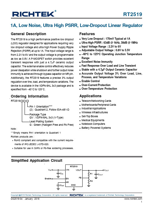
RT2519®Copyright 2018 Richtek Technology Corporation. All rights reserved. is a registered trademark of Richtek Technology Corporation.©1A, Low Noise, Ultra High PSRR, Low-Dropout Linear RegulatorGeneral DescriptionThe RT2519 is a high performance positive low dropout (LDO) regulator designed for applications requiring very low dropout voltage and ultra high Power Supply Ripple Rejection (PSRR) at up to 1A. The input voltage range is from 2.2V to 6V and the output voltage is programmable as low as 0.8V. A P-MOSFET switch provides excellent transient response with just a 4.7μF ceramic output capacitor. The external enable control effectively reduces power dissipation while shutdown and further output noise immunity is achieved through bypass capacitor on NR pin.Additionally, the RT2519 features a precise 3% output regulation over line, load, and temperature variations. The device is available in the VDFN-8AL 3x3 package and is specified from −40°C to 125°C.Features●Very Low Dropout : 170mV Typical at 1A●Ultra High PSRR : 63dB @ 1kHz, 38dB @ 1MHz ●Input Voltage Range : 2.2V to 6V●Adjustable Output Voltage : 0.8V to 5.5V●−40°C to 125°C Operating Junction Temperature Range●Excellent Noise Immunity●Fast Response Over Load and Line Transient ●Stable with a 4.7μF Output Ceramic Capacitor ●Accurate Output Voltage 3% Over Load, Line,Process, and Temperature Variations ●Enable Control●Over-Current Protection●Over-Temperature ProtectionOrdering InformationSimplified Application CircuitApplications●T elecom/Networking Cards ●Motherboards/Peripheral Cards ●Industrial Applications ●Wireless Infrastructures ●Set-Top Boxes●Medical Equipments ●Notebook Computers●Battery Powered SystemsNote :***Empty means Pin1 orientation is Quadrant 1Richtek products are :❝ RoHS compliant and compatible with the current require-ments of IPC/JEDEC J-STD-020.❝ Suitable for use in SnPb or Pb-free soldering processes.VOUTRT2519G : Green (Halogen Free and Pb Free)***RT2519©Copyright 2018 Richtek Technology Corporation. All rights reserved. is a registered trademark of Richtek Technology Corporation.Functional Pin DescriptionFunctional Block DiagramPin Configuration(TOP VIEW)VDFN-8AL 3x3FB KN= : Product CodeYMDNN : Date CodeVOUT FB VOUT GNDVIN VIN ENNRRT2519©Copyright 2018 Richtek Technology Corporation. All rights reserved. is a registered trademark of Richtek Technology Corporation.OperationThe RT2519 is a low noise, high PSRR LDO which supports very low dropout operation. The operating input range from 2.2V to 6V and the output voltage is programmable as low to 0.8V and the output current can be up to 1A. The internal compensation network is well designed to achieve fast transient response with good stability.In steady-state operation, the feedback voltage is regulated to the reference voltage by the internal regulator.When the feedback voltage signal is less than the reference, the output current passes through the power MOSFET will be increased. The extra amount of the current is sent to the output until the voltage level of FB pin returns to the reference.On the other hand, if the feedback voltage is higher than the reference, the power MOSFET current is decreased.The excess charge at the output can be released by the loading current.Start-UpThe RT2519 has a quick-start circuit to charge the noise reduction capacitor (C NR ). The switch of the quick-start circuit is closed at start up.To reduce the noise from bandgap, there is a low-pass (RC) filter consist of the C NR and the resistance which is connected with bandgap, as Functional Block Diagrams present.At the start-up, the quick-start switch is closed, with only 35k Ω resistance between bandgap and NR pin. The quick-start switch opens approximate 2ms after the device is enabled, the resistance between NR and bandgap is about 224k Ω to form a very good low pass filter and with great noise reduction performance.The 35k Ω resistance is used to slow down the reference voltage ramp to avoid inrush current at chip start-up, and the start-up time can be calculated as :t SS (sec) = 160000 x C NR (F) (1)It is recommend the C NR value larger than 0.01μF to reduce noise, and low leakage ceramic capacitors are suitable.However, with too large C NR will extend the start-up time very long if the C NR is not fully charged during 2ms andopens the quick-start switch, the C NR will be chargedthrough higher resistance 224k Ω and takes much longer time to finish the start up process.Enable and Shutdown OperationThe RT2519 goes into sleep mode when the EN pin is in a logic low condition. In this condition, the pass transistor,error amplifier, and bandgap are all turned off, reducing the supply current to only 2μA (max.). If the shutdown mode is not required, the EN pin can be directly tied to VIN pin to keep the LDO on.Current LimitThe RT2519 continuously monitors the output current to protect the pass transistor against abnormal operations.When an overload or short circuit is encountered, the current limit circuitry controls the pass transistor's gate voltage to limit the output within the predefined range. By reason of the build-in body diode, the pass transistor conducts current when the output voltage exceeds input voltage. Since the current is not limited, external current protection should be added if device may work at reverse voltage state.Over-Temperature Protection (OTP)The RT2519 has an over-temperature protection. When the device triggers the OTP , the device shuts down until the temperature back to normal state.Under Voltage Lock-Out (UVLO)The RT2519 utilizes an under voltage lock-out circuit to keep the output shut off until the internal circuitry is operating properly. The UVLO circuit has a de-glitch feature so that it typically ignores undershoot transients on the input if they are less than 30μs duration.RT2519©Copyright 2018 Richtek Technology Corporation. All rights reserved. is a registered trademark of Richtek Technology Corporation.Electrical Characteristics(V IN = V OUT + 0.5V or 2.2V , V OUT = 0.8V and 5.5V, I OUT = 1mA, V EN = 2.2V , C NR = 10nF , C OUT = 4.7μF , T J = −40°C to 125°C, unless otherwise specified)Absolute Maximum Ratings (Note 1)●All Pins ---------------------------------------------------------------------------------------------------------------------- −0.3V to 7V ●Power Dissipation, P D @ T A = 25°CVDFN-8AL 3x3-------------------------------------------------------------------------------------------------------------3.31W●Package Thermal Resistance (Note 2)VDFN-8AL 3x3, θJA --------------------------------------------------------------------------------------------------------30.2°C/W VDFN-8AL 3x3, θJC -------------------------------------------------------------------------------------------------------5.5°C/W ●Lead Temperature (Soldering, 10 sec.)-------------------------------------------------------------------------------260°C ●Junction T emperature -----------------------------------------------------------------------------------------------------150°C●Storage T emperature Range -------------------------------------------------------------------------------------------- −65°C to 150°C ●ESD Susceptibility (Note 3)HBM (Human Body Model)----------------------------------------------------------------------------------------------2kV CDM (Charged Device Model)------------------------------------------------------------------------------------------1kVRecommended Operating Conditions (Note 4)●Supply Voltage, VIN ------------------------------------------------------------------------------------------------------2.2V to 6V●Junction T emperature Range -------------------------------------------------------------------------------------------- −40°C to 125°CRT2519Copyright 2018 Richtek Technology Corporation. All rights reserved. is a registered trademark of Richtek Technology Corporation.RT2519©Copyright 2018 Richtek Technology Corporation. All rights reserved. is a registered trademark of Richtek Technology Corporation.Typical Application CircuitNote 1. Stresses beyond those listed “Absolute Maximum Ratings ” may cause permanent damage to the device. These arestress ratings only, and functional operation of the device at these or any other conditions beyond those indicated in the operational sections of the specifications is not implied. Exposure to absolute maximum rating conditions may affect device reliability.Note 2. θJA is measured under natural convection (still air) at T A = 25°C with the component mounted on a high effective-thermal-conductivity four-layer test board on a JEDEC 51-7 thermal measurement standard. θJC is measured at the exposed pad of the package.Note 3. Devices are ESD sensitive. Handling precaution is recommended.Note 4. The device is not guaranteed to function outside its operating conditions.Note 5. The spec. doesn't cover the tolerances from external resistors, and which is not tested at condition of V OUT = 0.8V, 4.5V≤ V IN ≤ 6V, and 750mA ≤ I OUT ≤ 1A since the power dissipation of the device is totally higher than the maximum rating of the package to lead a thermal shutdown issue.Note : All input and output capacitance in the suggested parameter mean the effective capacitance. The effectivecapacitance needs to consider any De-rating Effect like DC bias.V OUTRT2519©Copyright 2018 Richtek Technology Corporation. All rights reserved. is a registered trademark of Richtek Technology Corporation.Typical Operating Characteristics0.00.51.01.52.02.5-50-25255075100125Temperature (°C)S h u t d o w n C u r r e n t (μA )Reference Voltage vs. Temperature0.7900.7950.8000.8050.810-50-25255075100125Temperature (°C)R e f e r e n c e V o l t a g e (V )UVLO vs. Temperature1.51.61.71.81.92.02.12.2-50-25255075100125Temperature (°C)U V L O (V )PSRR vs. Frequency10203040506070809010 100 1k10k100k1M10MFrequency (Hz)P S R R (d B )Dropout Voltage vs. Output Current0501001502002004006008001000Output Current (mA)D r o p o u t V o l t a g e (m V )Dropout Voltage vs. Input Voltage05010015020023456Input Voltage (V)D r o p o u t V o l t a g e (m V )RT2519©Copyright 2018 Richtek Technology Corporation. All rights reserved. is a registered trademark of Richtek Technology Corporation.Time (50μs/Div)Power Off from ENV OUT (1V/Div)V EN (2V/Div)I OUT(500mA/Div)V IN = 4.3V, V OUT = 3.3VTime (500μs/Div)Power On from ENV OUT (1V/Div)V EN (2V/Div)I OUT(500mA/Div)V IN = 4.3V, V OUT = 3.3VTime (50μs/Div)Load Transient ResponseV OUT (50mV/Div)I OUT(500mA/Div)V IN = 4.3V, V OUT = 3.3V,I OUT = 0.1A to 1A (1A/μs, only shows the transient component)Time (50μs/Div)Line Transient Response V OUT (5mV/Div)V IN (1V/Div)V IN = 3.8V to 4.8V, V OUT = 3.3V,I OUT = 0.1AOutput Spectral Noise Density0.010.101.0010.00100.0010100100010000100000Frequency (Hz)O u t p u t S p e c t r a l N o i s e D e n s i t y (μV /√H z )RT2519©Copyright 2018 Richtek Technology Corporation. All rights reserved. is a registered trademark of Richtek Technology Corporation.Application InformationThe RT2519 is a low voltage, low dropout linear regulator with input voltage from 2.2V to 6V and a fixed output voltage from 0.8V to 5.5V.Dropout VoltageThe dropout voltage refers to the voltage difference between the VIN and VOUT pins while operating at specific output current. The dropout voltage V DO also can be expressed as the voltage drop on the pass-FET at specific output current(I RATED ) while the pass-FET is fully operating at ohmic region and the pass-FET can be characterized as an resistance R DS(ON). Thus the dropout voltage can be defined as (V DO = V VIN − V VOUT = R DS(ON) x I RATED ).For normal operation, the suggested LDO operating range is (V VIN > V VOUT + V DO ) for good transient response and PSRR ability. Vice versa, while operating at the ohmic region will degrade these performance severely.Output Voltage SettingFor the RT2519, the voltage on the FB pin sets the output voltage and is determined by the values of R1 and R2.The values of R1 and R2 can be calculated for any voltage using the formula given in Equation :()OUT R1 + R2V =0.8R2⨯Using lower values for R1 and R2 is recommended to reduces the noise injected from the FB pin. Note that R1is connected from VOUT pin to FB pin, and R2 is connected from FB to GND.Chip Enable OperationThe EN pin is the chip enable input. Pull the EN pin low (<0.4V) will shutdown the device. During shutdown mode,the RT2519 quiescent current drops to lower than 2μA.Drive the EN pin to high (>1.2V, <6V) will turn on the device again. For external timing control (e.g.RC), the EN pin can also be externally pulled to High by adding a 100k Ωor greater resistor from the VIN pin.Current LimitThe RT2519 continuously monitors the output current to protect the pass transistor against abnormal operations.When an overload or short circuit is encountered, thecurrent limit circuitry controls the pass transistor's gatevoltage to limit the output within the predefined range. By reason of the build-in body diode, the pass transistor conducts current when the output voltage exceeds input voltage. Since the current is not limited, external current protection should be added if device may work at reverse voltage state.C IN and C OUT SelectionLike any low dropout regulator, the external capacitors of the RT2519 must be carefully selected for regulator stability and performance. Using a capacitor of at least 4.7μF is suitable. The input capacitor must be located at a distance of no more than 0.5 inch from the input pin of the chip.Any good quality ceramic capacitor can be used. However,a capacitor with larger value and lower ESR (Equivalent Series Resistance) is recommended since it will provide better PSRR and line transient response.The RT2519 is designed specifically to work with low ESR ceramic output capacitor for space saving and performance consideration. Using a ceramic capacitor with capacitance of at least 4.7μF on the RT2519 output ensures stability.Output NoiseGenerally speaking, the dominant noise source is from the internal bandgap for most LDOs. With the noise reduction capacitor connecting to the NR pin of the RT2519, the noise component contributed from bandgap will not be significantly. Instead, the most noise source comes from the output resistor divider and the error amplifier input. For general application to minimize noise,using a 0.01μF noise-reduction capacitor (C NR ) is recommended.Thermal ConsiderationsThermal protection limits power dissipation in the RT2519.When the operation junction temperature exceeds 160°C,the OTP circuit starts the thermal shutdown function and turns the pass element off. The pass element turns on again after the junction temperature cools down by 20°C.The RT2519 output voltage will be closed to zero when output short circuit occurs as shown in Figure 1. It canRT2519©Copyright 2018 Richtek Technology Corporation. All rights reserved. is a registered trademark of Richtek Technology Corporation.reduce the chip temperature and provides maximum safety to end users when output short circuit occurs.The junction temperature should never exceed theabsolute maximum junction temperature T J(MAX), listed under Absolute Maximum Ratings, to avoid permanent damage to the device. The maximum allowable power dissipation depends on the thermal resistance of the IC package, the PCB layout, the rate of surrounding airflow,and the difference between the junction and ambient temperatures. The maximum power dissipation can be calculated using the following formula :P D(MAX) = (T J(MAX) − T A ) / θJAwhere T J(MAX) is the maximum junction temperature, T A is the ambient temperature, and θJA is the junction-to-ambient thermal resistance.For continuous operation, the maximum operating junction temperature indicated under Recommended Operating Conditions is 125°C. The junction-to-ambient thermal resistance, θJA , is highly package dependent. For a VDFN-8AL 3x3 package, the thermal resistance, θJA , is 30.2°C/W on a standard JEDEC 51-7 high effective-thermal-conductivity four-layer test board. The maximum power dissipation at T A = 25°C can be calculated as below :P D(MAX) = (125°C − 25°C) / (30.2°C/W) = 3.31W for a VDFN-8AL 3x3 package.The maximum power dissipation depends on the operating ambient temperature for the fixed T J(MAX) and the thermal resistance, θJA . The derating curves in Figure 2 allowsFigure 1. Short-Circuit Protection when Output Short-Circuit Occurs V OUT Short to GNDV OUTI OUTthe designer to see the effect of rising ambient temperature on the maximum power dissipation.Figure 2. Derating Curve of Maximum Power Dissipation0.00.81.62.43.24.00255075100125Ambient Temperature (°C)M a x i m u m P o w e r D i s s i p a t i o n (W )RT251911DS2519-04 January 2018©Copyright 2018 Richtek Technology Corporation. All rights reserved. is a registered trademark of Richtek Technology yout ConsiderationFigure 3. PCB Layout Guide12DS2519-04 January 2018 Richtek Technology Corporation14F, No. 8, Tai Yuen 1st Street, Chupei City Hsinchu, Taiwan, R.O.C.Tel: (8863)5526789Richtek products are sold by description only. Customers should obtain the latest relevant information and data sheets before placing orders and should verify that such information is current and complete. Richtek cannot assume responsibility for use of any circuitry other than circuitry entirely embodied in a Richtek product. Information furnished by Richtek is believed to be accurate and reliable. However, no responsibility is assumed by Richtek or its subsidiaries for its use;nor for any infringements of patents or other rights of third parties which may result from its use. No license is granted by implication or otherwise under any patent or patent rights of Richtek or its subsidiaries.V-Type 8AL DFN 3x3 Package。
Elite Semiconductor EMP8041 高电压低功耗低掉落线性调节器说明书

High Input Voltage, Low Quiescent Current, Low-Dropout Linear RegulatorGeneral DescriptionThe EMP8041 is a high voltage, low quiescent current, low dropout regulator with 150mA output driving capacity. The EMP8041, which operates over an input range of 3V to 40V, is stable with any capacitors, whose capacitance is larger than 1 F, and suitable for powering battery-management ICs because of the virtue of its low quiescent current consumption and low dropout voltage. Below the maximum power dissipation (please refer to Note. 5), It guarantees delivery of 100mA output current, and supports preset output voltages ranging from 1.3V to 6.0V with 0.1V increment.EMP8041 features also include bandgap voltage reference, constant current limiting and thermal overload protection. Both miniature SOT-23-5 and SOT-89-3 package options are offered to provide flexibility for different applications. ApplicationsLogic Supply for High Voltage BatteriesKeep-Alive Supply3-4 Cell Li-ion Batteries Powered systemsFeatures150mA output current driving capacity780mV typical dropout at Io=150mA12µA typical quiescent current1µA typical shutdown mode3.0V to 40V input rangeStable with small ceramic output capacitors (1µF)Over temperature and over currentprotection±2.5% output voltage toleranceTypical ApplicationConnection DiagramsOrder informationEMP8041-XXVF05NRR XX Output voltage VF05 SOT-23-5 Package NRR RoHS & Halogen free packageRating: -40 to 85°CPackage in Tape & ReelEMP8041-XXVG03NRR XX Output voltage VG03 SOT-89-3 Package NRR RoHS & Halogen free packageRating: -40 to 85°CPackage in Tape & ReelOrder, Marking and Packing InformationPackageSOT-23-5SOT-89-38041Tracking Code132PIN1 DOTPin FunctionsNameSOT-23-5SOT-89-3FunctionV IN 1 3 Supply Voltage InputRequire a minimum input capacitor of close to 1µF to ensure stability andsufficient decoupling from the ground pin.GND 2 2 Ground PinEN 3 N/A Shutdown InputThe EN pin is pulled “High” internally. Set the regulator into the disable mode bypulling the EN pin low.NC 4 N/A No connection V OUT 51 Output VoltageFunctional Block DiagramV INENV OUTFIG.1. Functional Block Diagram of EMP8041Absolute Maximum Ratings (Notes 1, 2)V IN , EN -0.3V to 42V V OUT -0.3V to 13.2V Power Dissipation (Note 3) Storage Temperature Range -65°C to 150°CJunction Temperature (T J ) 160°C Lead Temperature (Soldering, 10 sec.) 260°C ESD RatingHuman Body Model 2KVOperating Ratings (Note 1, 2)Supply Voltage 3.0V to 40V Operating Temperature Range -40°C to 85°C Thermal Resistance (θJA , Note 3)) 152°C/W (SOT-23-5)90°C/W (SOT-89-3)Thermal Resistance (θJC, Note 4)) 81°C/W (SOT-23-5)52°C/W (SOT-89-3)Electrical CharacteristicsT A = 25°C, V OUT (NOM)=5V; unless otherwise specified, all limits guaranteed for V IN = V OUT +1V, C IN = C OUT =1µF.SymbolParameterConditionsMinTyp (Note 6)Max Units V IN Input Voltage 3.040VΔV OTL Output Voltage ToleranceI OUT = 10mAV OUT (NOM) +1V ≤ V IN ≤ 40V -2.5 +2.5% ofV OUT (NOM) I OUT Maximum Output Current Average DC Current Rating 150 mA I LIMITOutput Current Limit300 mAI OUT = 0.1mA12 30 I OUT = 100mA 50 100 Supply CurrentI OUT = 150mA 80 130 I QShutdown Supply Current V OUT = 0V, EN = GND 1 5 µA I OUT = 30mA 135 I OUT = 100mA 500 V DODropout Voltage V OUT =5.0V (Note. 7)I OUT = 150mA780mV Line RegulationI OUT = 1mA,(V OUT + 1V) ≤ V IN ≤ 40V0.1 % ΔV OUTLoad Regulation0.1mA ≤ I OUT ≤ 100mA0.5 %e n Output Voltage NoiseI OUT =10mA,10Hz ≤ f ≤ 100kHzV OUT = 5.0V 800 µV RMSV IH , (V OUT + 1V) ≤ V IN ≤ 40V 1.0 V EN EN Input ThresholdV IL , (V OUT + 1V) ≤ V IN ≤ 40V0.3VI EN EN Input Bias Current EN = GND or V IN0.1 µAThermal ShutdownTemperature 160T SDThermal Shutdown Hysteresis30 ℃t ON Start-Up Time C OUT = 1.0µF, V OUT at 90% of Final Value500µsNote 1: Absolute maximum ratings indicate limits beyond which damage may occur.Note 2: All voltages are in respect to the potential of the ground pin.Note 3: θJA is measured in the natural convection at T A =25℃ on a high effectively thermal conductivity test board (2layers, 2S0P).Note 4: θJC represents the resistance between the chip and the top of the package case.Note 5: Maximum power dissipation for the device is calculated using the following equation:JAθAT - J(MAX)TD PWhere T J (MAX) is the maximum junction temperature, T A is the ambient temperature, and θJA is the junction-to-ambient thermal resistance. For example, for the SOT-89-3 package θJA =90°C/W, T J (MAX)=160°C and using T A =25°C, the maximum power dissipation is 1.5W.The derating factor (-1/θJA )=-11.1mW/°C. Below 25°C the power dissipation figure can be increased by 11.1mW per degree and similarly decreased by this factor for temperatures above 25°C.Note 6: Typical values represent the most likely parametric norm.Note 7: Dropout voltage is measured by reducing V IN until V OUT drops to 98% its nominal value.Typical Performance CharacteristicsUnless otherwise specified, V IN = V OUT (NOM) + 1V, V OUT=5V, C IN = C OUT = 1.0µF, T A = 25°C, EN = 2VTypical Performance Characteristics (cont.)Unless otherwise specified, V IN = V OUT (NOM) + 1V, V OUT =5V, C IN = C OUT = 1.0µF, T A = 25°C~400us~400usLine transient (I OUT =1mA)Line transient (I OUT =30mA)Vin (1V/div)Vout (20mV/div)Time (100us/div)Vin (1V/div)Vout (50mV/div)Time (100us/div)Load transient (V OUT =5.0V)Load transient (V OUT =5.0V)Vout (200mV/div)Iout (50mA/div)Time (100us/div)Application InformationGeneral DescriptionReferring to Fig.1 as shown in the Functional Block Diagram section, the EMP8041 adopts the classical regulator topology in which negative feedback control is used to perform the desired voltage regulating function. The negative feedback is formed by using feedback resistors (R1, R2) to sample the output voltage for the non-inverting input of the error amplifier, whose inverting input is set to the bandgap reference voltage. By the virtue of its high open-loop gain, the error amplifier operates to ensure that the sampled output feedback voltage at its non-inverting input is virtually equal to the preset bandgap reference voltage.The error amplifier compares the voltage difference at its inputs and produces an appropriate driving voltage to the P-channel MOS pass transistor to control the amount of current reaching the output. If there are changes in the output voltage due to load changes, the feedback resistors register such changes to the non-inverting input of the error amplifier. The error amplifier then adjusts its driving voltage to maintain virtual short between its two input nodes under all loading conditions. In a nutshell, the regulation of the output voltage is achieved as a direct result of the error amplifier keeping its input voltages equal. This negative feedback control topology is further augmented by the shutdown, the fault detection, and the temperature and current protection circuitry.Output CapacitorThe EMP8041 is specially designed for use with ceramic output capacitors of as low as 1.0µF to take advantage of the savings in cost and space as well as the superior filtering of high frequency noise. Capacitors of higher value or other types may be used, but it is important to make sure its equivalent series resistance (ESR) is restricted to less than 0.5Ω. The use of larger capacitors with smaller ESR values is desirable for applications involving large and fast input or output transients, as well as for situations where the application systems are not physically located immediately adjacent to the battery power source. Typical ceramic capacitors suitable for use with the EMP8041 are X5R and X7R. The X5R and the X7R capacitors are able to maintain their capacitance values to within ±20% and ±10%, respectively, as the temperature increases.No-Load StabilityThe EMP8041 is capable of stable operation during no-load conditions, a mandatory feature for some applications such as CMOS RAM keep-alive operations.Input CapacitorA minimum input capacitance of 1µF is required for EMP8041. The capacitor value may be increased without limit. Improper workbench set-ups may have adverse effects on the normal operation of the regulator. A case in point is the instability that may result from long supply lead inductance coupling to the output through the gate capacitance of the pass transistor. This will establish a pseudo LCR network, and is likely to happen under high current conditions or near dropout. A 10µF tantalum input capacitor will dampen the parasitic LCR action thanks to its high ESR. However, cautions should be exercised to avoid regulator short-circuit damage when tantalum capacitors are used, for they are prone to fail in short-circuit operating conditions.Power Dissipation and Thermal ShutdownThermal overload results from excessive power dissipation that causes the IC junction temperature to increase beyond a safe operating level. The EMP8041 relies on dedicated thermal shutdown circuitry to limit its total power dissipation. An IC junction temperature T J exceeding 160°C will trigger the thermal shutdown logic, turning off the P-channel MOS pass transistor. The pass transistor turns on again after the junction cools off by about 30°C. When continuous thermal overload conditions persist, this thermal shutdown action then results in a pulsed waveform at the output of the regulator. The concept of thermal resistance θJA (°C/W) is often used to describe an IC junction’s relative readiness in allowing its thermal energy to dissipate to its ambient air. An IC junction with a low thermal resistance is preferred because it is relatively effective in dissipating its thermal energy to its ambient, thus resulting in a relatively low and desirable junction temperature. The relationship between θJA and T J is as follows:T J = θJA x (P D) + T AT A is the ambient temperature, and P D is the power generated by the IC and can be written as:P D = I OUT (V IN - V OUT)As the above equations show, it is desirable to work with ICs whose θJA values are small such that T J does not increase strongly with P D. To avoid thermally overloading the EMP8041, refrain from exceeding the absolute maximum junction temperature rating of 160°C under continuous operating conditions. Overstressing the regulator with high loading currents and elevated input-to-output differential voltages can increase the IC die temperature significantly.ShutdownThe EMP8041 enters the sleep mode when the EN pin is low. When this occurs, the pass transistor, the error amplifier, and the biasing circuits, including the bandgap reference, are turned off, thus reducing the supply current to typically 1µA. Such a low supply current makes the EMP8041 best suited for battery-powered applications. The maximum guaranteed voltage at the EN pin for the sleep mode to take effect is 0.3V. The EN pin is pulled high internally.ESMTEMP8041Package Outline Drawing SOT-23-5TOP VIEWSIDE VIEWMARKDETAIL AAPackage Outline DrawingSOT-89-3Min1.40.40.354.4Dimension in mmRevision HistoryRevisionDateDescription0.1 2010.05.05 Original0.2 2010.8.271) Updated output voltage option 2) Revised Iq spec. 1.0 2011.2.23 Skip “Preliminary”1.1 2011.12.13 1) Modified 100mA output driving capacity to 150mA.2) Modified the output voltage accuracy is based onIout=10mA this condition.3) Added Iout=150mA spec. into electrical characteristics table. 1.2 2012.03.291) Modified the operating voltage from 36V to 40V.2) Modified the absolute maximum ratings V IN , EN from40V to 42V.3) Updated the package outline drawing. 1.32013.10.17Modify package outline drawingImportant NoticeAll rights reserved.No part of this document may be reproduced or duplicated in any form or by any means without the prior permission of ESMT.The contents contained in this document are believed to be accurate at the time of publication. ESMT assumes no responsibility for any error in this document, and reserves the right to change the products or specification in this document without notice.The information contained herein is presented only as a guide or examples for the application of our products. No responsibility is assumed by ESMT for any infringement of patents, copyrights, or other intellectual property rights of third parties which may result from its use. No license, either express , implied or otherwise, is granted under any patents, copyrights or other intellectual property rights of ESMT or others.Any semiconductor devices may have inherently a certain rate of failure. To minimize risks associated with customer's application, adequate design and operating safeguards against injury, damage, or loss from such failure, should be provided by the customer when making application designs. ESMT's products are not authorized for use in critical applications such as, but not limited to, life support devices or system, where failure or abnormal operation may directly affect human lives or cause physical injury or property damage. If products described here are to be used for such kinds of application, purchaser must do its own quality assurance testing appropriate to such applications.。
稳压芯片AMS1117-5.0

OPERATING JUNCTION TEMPERATURE RANGE -40 to 125° C -40 to 125° C -40 to 125° C -40 to 125° C -40 to 125° C -40 to 125° C -40 to 125° C
8L SOIC Top View
Advanced Monolithic Systems
FEATURES
• Three Terminal Adjustable or Fixed Voltages* 1.5V, 1.8V, 2.5V, 2.85V, 3.3V and 5.0V • Output Current of 1A • Operates Down to 1V Dropout • Line Regulation: 0.2% Max. • Load Regulation: 0.4% Max. • SOT-223, TO-252 and SO-8 package available
Load Regulation (Notes 2, 3)
AMS1117 AMS1117-1.5 AMS1117-1.8 AMS1117-2.5
Advanced Monolithic Systems, Inc.
Phone (925) 443-0722
GENERAL DESCRIPTION
The AMS1117 series of adjustable and fixed voltage regulators are designed to provide 1A output current and to operate down to 1V input-to-output differential. The dropout voltage of the device is guaranteed maximum 1.3V at maximum output current, decreasing at lower load currents. On-chip trimming adjusts the reference voltage to 1%. Current limit is also trimmed, minimizing the stress under overload conditions on both the regulator and power source circuitry. The AMS1117 devices are pin compatible with other three-terminal SCSI regulators and are offered in the low profile surface mount SOT-223 package, in the 8L SOIC package and in the TO-252 (DPAK) plastic package.
PT5108

3.0
PT5108E23E-30
3.1PT51ຫໍສະໝຸດ 8E23E-313.2PT5108E23E-32
3.3
PT5108E23E-33
4.7
PT5108E23E-47
4.8
PT5108E23E-48
4.9
PT5108E23E-49
5.0
PT5108E23E-50
2.0
PT5108E23E-20
* All parts are supplied as 3000 units, tape and reel.
PACKAGES
VEN
GND
VIN
3
2
1
PT5108
4
BYPASS SOT 23-5
5
VOUT
PT5108
High-PSRR 500mA LDO
PIN DESCRIPTIONS
Name
SOT-23
VIN
1
GND
2
VEN
3
BYPASS
4
VOUT
5
Description Input of LDO Ground Enable Input Logic, Enable High Optional bypass capacitor for noise reduction
FEATURES
APPLICATIONS
2.5V to 5.5V input range
CDMA/GSM mobile phone
72dB PSRR @1kHz, Vin = Vout + 1V
Handless telephone
< 1uA quiescent current at shutdown mode
AMS1117-3V3

Advanced AMS1117 Monolithic 1A LOW DROPOUT VOLTAGE REGULATOR SystemsRoHS compliantFEATURES APPLICATIONS• Three Terminal Adjustable or Fixed Voltages* • High Efficiency Linear Regulators1.5V, 1.8V,2.5V, 2.85V,3.3V and 5.0V •Post Regulators for Switching Supplies• Output Current of 1A • 5V to 3.3V Linear Regulator• Operates Down to 1V Dropout • Battery Chargers• Line Regulation: 0.2% Max. • Active SCSI Terminators• Load Regulation: 0.4% Max. • Power Management for Notebook• SOT-223, TO-252 and SO-8 package available • Battery Powered InstrumentationGENERAL DESCRIPTIONThe AMS1117 series of adjustable and fixed voltage regulators are designed to provide 1A output current and to operate down to 1V input-to-output differential. The dropout voltage of the device is guaranteed maximum 1.3V at maximum output current, decreasing at lower load currents.On-chip trimming adjusts the reference voltage to 1%. Current limit is also trimmed, minimizing the stress under overload conditions on both the regulator and power source circuitry.The AMS1117 devices are pin compatible with other three-terminal SCSI regulators and are offered in the low profile surface mount SOT-223 package, in the 8L SOIC package and in the TO-252 (DPAK) plastic package.ORDERING INFORMATION:PACKAGE TYPEOPERATING JUNCTION TO-252 SOT-223 8L SOIC TEMPERATURE RANGEAMS1117CD AMS1117 AMS1117CS -40 to 125°CAMS1117CD-1.5 AMS1117-1.5 AMS1117CS-1.5 -40 to 125° CAMS1117CD-1.8 AMS1117-1.8 AMS1117CS-1.8 -40 to 125° CAMS1117CD-2.5 AMS1117-2.5 AMS1117CS-2.5 -40 to 125° CAMS1117CD-2.85 AMS1117-2.85 AMS1117CS-2.85 -40 to 125° CAMS1117CD-3.3 AMS1117-3.3 AMS1117CS-3.3 -40 to 125° CAMS1117CD-5.0 AMS1117-5.0 AMS1117CS-5.0 -40 to 125° C*For additional available fixed voltages contact factory.PIN CONNECTIONSSOT-223 Top View3 PIN FIXED/ADJUSTABLEVERSION1- Ground/Adjust2- V OUT3- V INAMS1117ABSOLUTE MAXIMUM RATINGS (Note 1)Power DissipationInternally limited Soldering information Input Voltage15V Lead Temperature (25 sec) 265°C Operating Junction TemperatureThermal Resistance Control Section0°C to 125°C SO-8 package ϕ JA = 160°C/W Power Transistor0°C to 150°C TO-252 package ϕ JA = 80°C/W Storage temperature- 65°C to +150°C SOT-223 package ϕ JA = 90°C/W** With package soldering to copper area over backsideground plane or internal power plane ϕ JA can vary from46°C/W to >90°C/W depending on mounting technique andthe size of the copper area.ELECTRICAL CHARACTERISTICS Electrical Characteristics at I OUT = 0 mA, and T J = +25°C unless otherwise specified.ParameterDevice Conditions Min Typ Max Units Reference Voltage(Note 2)AMS1117 I OUT = 10 mA 10mA ≤ I OUT ≤ 1A, 1.5V ≤ (V IN - V OUT ) ≤ 12V 1.238 1.225 1.250 1.250 1.262 1.270 V V Output Voltage(Note 2)AMS1117-1.5 0 ≤ I OUT ≤ 1A , 3.0V ≤ V IN ≤ 12V 1.485 1.476 1.500 1.500 1.515 1.524 V VAMS1117-1.8 0 ≤ I OUT ≤ 1A , 3.3V ≤ V IN ≤ 12V 1.782 1.773 1.800 1.800 1.818 1.827 V VAMS1117-2.5 0 ≤ I OUT ≤ 1A , 4.0V ≤ V IN ≤ 12V 2.475 2.460 2.500 2.500 2.525 2.560 V VAMS1117-2.85 0 ≤ I OUT ≤ 1A , 4.35V ≤ V IN ≤ 12V 2.82 2.79 2.850 2.850 2.88 2.91 V VAMS1117-3.3 0 ≤ I OUT ≤ 1A , 4.75V ≤ V IN ≤ 12V 3.267 3.235 3.300 3.300 3.333 3.365 V V AMS1117-5.0 0 ≤ I OUT ≤ 1A , 6.5V ≤ V IN ≤ 12V 4.9504.9005.000 5.000 5.050 5.100 V VLine Regulation AMS1117 I LOAD = 10 mA , 1.5V ≤ (V IN - V OUT ) ≤ 12V 0.015 0.035 0.2 0.2 %%AMS1117-1.5 3.0V ≤ V IN ≤ 12V 0.3 0.6 5 6 mVmVAMS1117-1.8 3.3V ≤ V IN ≤ 12V 0.3 0.6 5 6 mVmVAMS1117-2.5 4.0V ≤ V IN ≤ 12V 0.3 0.6 6 6 mVmVAMS1117-2.85 4.35V ≤ V IN ≤ 12V 0.3 0.6 6 6 mVmVAMS1117-3.3 4.75V ≤ V IN ≤ 12V 0.5 1.0 10 10 mVmVAMS1117-5.0 6.5V ≤ V IN ≤ 12V 0.5 1.0 10 10 mVmVLoad Regulation (Notes 2, 3) AMS1117 (V IN - V OUT ) =3V, 10mA ≤ I OUT ≤ 1A 0.1 0.2 0.3 0.4 %%AMS1117-1.5 V IN = 5V, 0 ≤ I OUT ≤ 1A 3 6 10 20 mVmVAMS1117-1.8 V IN = 5V, 0 ≤ I OUT ≤ 1A 3 6 10 20 mVmVAMS1117-2.5 V IN = 5V, 0 ≤ I OUT ≤ 1A 3 6 1220mVmVAMS1117ELECTRICAL CHARACTERISTICS Electrical Characteristics at I OUT = 0 mA, and T J = +25°C unless otherwise specified.ParameterDevice Conditions Min Typ Max Units Load Regulation(Notes 2, 3)AMS1117-2.85 V IN = 5V, 0 ≤ I OUT ≤ 1A 3 6 12 20 mV mV AMS1117-3.3 V IN = 5V, 0 ≤ I OUT ≤ 1A3 7 15 25 mV mV AMS1117-5.0 V IN = 8V, 0 ≤ I OUT ≤ 1A5 10 20 35 mV mV Dropout Voltage(V IN - V OUT )AMS1117-1.5/-1.8/-2.5/-2.85/-3.3/-5.0 ∆V OUT , ∆V REF = 1%, I OUT = 1A (Note 4) 1.1 1.3 V Current LimitAMS1117-1.5/-1.8/-2.5/-2.85/-3.3/-5.0 (V IN - V OUT ) = 5V 900 1,100 1,500 mA Minimum LoadCurrentAMS1117 (V IN - V OUT ) = 12V (Note 5) 5 10 mA Quiescent CurrentAMS1117-1.5/-1.8/-2.5/-2.85/-3.3/-5.0 V IN ≤ 12V 5 10 mA Ripple RejectionAMS1117 f =120Hz , C OUT = 22µF Tantalum, I OUT = 1A, (V IN -V OUT ) = 3V, C ADJ =10µF 60 75 dB AMS1117-1.5/-1.8/-2.5/-2.85 f =120Hz , C OUT = 22µF Tantalum, I OUT = 1A, V IN = 6V 6072 dB AMS1117-3.3 f =120Hz , C OUT = 22µF Tantalum, I OUT = 1A V IN = 6.3V 60 72dB AMS1117-5.0 f =120Hz , C OUT = 22µF Tantalum, I OUT = 1A V IN = 8V 60 68dB Thermal Regulation AMS1117 T A = 25°C, 30ms pulse 0.008 0.04 %WAdjust Pin Current AMS1117 10mA ≤ I OUT ≤ 1A , 1.5V ≤ (V IN - V OUT ) ≤ 12V 55 120 µAµAAdjust Pin Current Change AMS1117 10mA ≤ I OUT ≤ 1A , 1.5V ≤ (V IN - V OUT ) ≤ 12V 0.2 5 µATemperature Stability 0.5 %Long Term Stability T A =125°C, 1000Hrs 0.3 1 %RMS Output Noise (% of V OUT )T A = 25°C , 10Hz ≤ f ≤ 10kHz 0.003 %Thermal ResistanceJunction-to-Case 15 °C/WParameters identified with boldface type apply over the full operating temperature range.Note 1: Absolute Maximum Ratings indicate limits beyond which damage to the device may occur. For guaranteed specifications and test conditions, see the Electrical Characteristics . The guaranteed specifications apply only for the test conditions listed.Note 2: Line and Load regulation are guaranteed up to the maximum power dissipation of 1.2 W. Power dissipation is determined by the input/output differential and the output current. Guaranteed maximum power dissipation will not be available over the full input/output range.Note 3: See thermal regulation specifications for changes in output voltage due to heating effects. Line and load regulation are measured at a constant junction temperature by low duty cycle pulse testing. Load regulation is measured at the output lead ~1/8” from the package.Note 4: Dropout voltage is specified over the full output current range of the device.Note 5: Minimum load current is defined as the minimum output current required to maintain regulation. When 1.5V ≤ (V IN - V OUT ) ≤ 12V the device is guaranteed to regulate if the output current is greater than 10mA.AMS1117 APPLICATION HINTSThe AMS1117 series of adjustable and fixed regulators are easy touse and are protected against short circuit and thermal overloads.Thermal protection circuitry will shut-down the regulator shouldthe junction temperature exceed 165°C at the sense point.Pin compatible with older three terminal adjustable regulators, these devices offer the advantage of a lower dropout voltage, more precise reference tolerance and improved reference stability with temperature.StabilityThe circuit design used in the AMS1117 series requires the use of an output capacitor as part of the device frequency compensation. The addition of22µF solid tantalum on the output will ensure stability for all operating conditions.When the adjustment terminal is bypassed with a capacitor to improve the ripple rejection, the requirement for an output capacitor increases. The value of 22µF tantalum covers all cases of bypassing the adjustment terminal. Without bypassing the adjustment terminal smaller capacitors can be used with equally good results.To further improve stability and transient response of these devices larger values of output capacitor can be used.Protection DiodesUnlike older regulators, the AMS1117 family does not need any protection diodes between the adjustment pin and the output and from the output to the input to prevent over-stressing the die. Internal resistors are limiting the internal current paths on the AMS1117 adjustment pin, therefore even with capacitors on the adjustment pin no protection diode is needed to ensure device safety under short-circuit conditions.Diodes between the input and output are not usually needed. Microsecond surge currents of 50A to 100A can be handled by the internal diode between the input and output pins of the device. In normal operations it is difficult to get those values of surge currents even with the use of large output capacitances. If high value output capacitors are used, such as 1000µF to 5000µF and the input pin is instantaneously shorted to ground, damage can occur. A diode from output to input is recommended, when a crowbar circuit at the input of the AMS1117 is used (Figure 1).FVOUTD1VINFigure 1.Output VoltageThe AMS1117 series develops a 1.25V reference voltage between the output and the adjust terminal. Placing a resistor between these two terminals causes a constant current to flow through R1 and down through R2 to set the overall output voltage. This current is normally the specified minimum load current of 10mA. Because I ADJ is very small and constant it represents a small error and it can usually be ignored.VOUT VINV OUT = V REF (1+ R2/R1)+I ADJ R2Figure 2. Basic Adjustable RegulatorLoad RegulationTrue remote load sensing it is not possible to provide, because the AMS1117 is a three terminal device. The resistance of the wire connecting the regulator to the load will limit the load regulation. The data sheet specification for load regulation is measured at the bottom of the package. Negative side sensing is a true Kelvin connection, with the bottom of the output divider returned to the negative side of the load.The best load regulation is obtained when the top of the resistor divider R1 is connected directly to the case not to the load. If R1 were connected to the load, the effective resistance between the regulator and the load would be:R P x( R2+R1 ) , R P = Parasitic Line Resistance R1AMS1117APPLICATION HINTSConnected as shown , R P is not multiplied by the divider ratioR LV IN R P PARASITIC*CONNECT R1 TO CASECONNECT R2 TO LOADFigure 3. Connections for Best Load RegulationIn the case of fixed voltage devices the top of R1 is connected Kelvin internally, and the ground pin can be used for negative side sensing. Thermal Considerations The AMS1117 series have internal power and thermal limiting circuitry designed to protect the device under overload conditions. However maximum junction temperature ratings of 125°C should not be exceeded under continuous normal load conditions. Careful consideration must be given to all sources of thermal resistance from junction to ambient. For the surface mount package SOT-223 additional heat sources mounted near the device must be considered. The heat dissipation capability of the PC board and its copper traces is used as a heat sink for the device. The thermal resistance from the junction to the tab for the AMS1117 is 15°C/W. Thermal resistance from tab to ambient canbe as low as 30°C/W. The total thermal resistance from junction to ambient can be as low as 45°C/W. This requires a reasonable sized PC board with at least on layer of copper to spread the heat across the board and couple it into the surrounding air. Experiments have shown that the heat spreading copper layer does not need to be electrically connected to the tab of the device. The PC material can be very effective at transmitting heat between the pad area, attached to the pad of the device, and a ground plane layer either inside or on the opposite side of the board. Although the actual thermal resistance of the PC material is high, the Length/Area ratio of the thermal resistance between layers is small. The data in Table 1, was taken using 1/16” FR-4 board with 1 oz. copper foil, and it can be used as a rough guideline for estimating thermal resistance. For each application the thermal resistance will be affected by thermal interactions with other components on the board. To determine the actual value some experimentation will be necessary. The power dissipation of the AMS1117 is equal to: P D = ( V IN - V OUT )( I OUT ) Maximum junction temperature will be equal to: T J = T A(MAX) + P D (Thermal Resistance (junction-to-ambient))Maximum junction temperature must not exceed 125°C.Ripple RejectionThe ripple rejection values are measured with the adjustment pin bypassed. The impedance of the adjust pin capacitor at the ripple frequency should be less than the value of R1 (normally 100Ω to 200Ω) for a proper bypassing and ripple rejection approaching the values shown. The size of the required adjust pin capacitor is a function of the input ripple frequency. If R1=100Ω at 120Hz the adjust pin capacitor should be >13µF. At 10kHz only 0.16µF is needed.The ripple rejection will be a function of output voltage, in circuits without an adjust pin bypass capacitor. The output ripple will increase directly as a ratio of the output voltage to the reference voltage (V OUT / V REF ).Table 1. COPPER AREA THERMAL RESISTANCETOP SIDE* BACK SIDE BOARD AREA (JUNCTION-TO-AMBIENT)2500 Sq. mm 2500 Sq. mm 2500 Sq. mm 45°C/W1000 Sq. mm 2500 Sq. mm 2500 Sq. mm 45°C/W225 Sq. mm 2500 Sq. mm 2500 Sq. mm 53°C/W100 Sq. mm 2500 Sq. mm 2500 Sq. mm 59°C/W1000 Sq. mm 1000 Sq. mm 1000 Sq. mm 52°C/W1000 Sq. mm 0 1000 Sq. mm55°C/W * Tab of device attached to topside copper.AMS1117TYPICAL PERFORMANCE CHARACTERISTICSMinimum Operating Current(Adjustable Device)Short-Circuit Current 036912M I N I M U M O P E R A T I N G C U R R E N T (m A )-0.20-0.15-0.10-0.0500.050.10O U T P U T V O L T A G E D E V I A T I O N (%)-50-250255075100125150-2.0-1.001.02.0TEMPERATURE (°C)O U T P U T V O L T A G E C H A N G E (%)TEMPERATURE (°C)-50-250255075100125150AMS1117 PACKAGE DIMENSIONS inches (millimeters) unless otherwise noted.TO-252 PLASTIC PACKAGE (D)3 LEAD SOT-223 PLASTIC PACKAGE8 LEAD SOIC PLASTIC PACKAGE (S)*DIMENSION DOES NOT INCLUDE MOLD FLASH. MOLD FLASHSHALL NOT EXCEED 0.006" (0.152mm) PER SIDE**DIMENSION DOES NOT INCLUDE INTERLEAD FLASH. INTERLEADFLASH SHALL NOT EXCEED 0.010" (0.254mm) PER SIDE。
AMS1117 pdf

Advanced AMS1117 Monolithic 1A LOW DROPOUT VOLTAGE REGULATORSystemsRoHS compliantFEATURESAPPLICATIONS• Three Terminal Adjustable or Fixed Voltages* • High Efficiency Linear Regulators1.5V, 1.8V,2.5V, 2.85V,3.3V and 5.0V •Post Regulators for Switching Supplies • Output Current of 1A• 5V to 3.3V Linear Regulator • Operates Down to 1V Dropout • Battery Chargers• Line Regulation: 0.2% Max. • Active SCSI Terminators• Load Regulation: 0.4% Max.• Power Management for Notebook • SOT-223, TO-252 and SO-8 package available • Battery Powered InstrumentationGENERAL DESCRIPTIONThe AMS1117 series of adjustable and fixed voltage regulators are designed to provide 1A output current and to operate down to 1V input-to-output differential. The dropout voltage of the device is guaranteed maximum 1.3V at maximum output current, decreasing at lower load currents.On-chip trimming adjusts the reference voltage to 1%. Current limit is also trimmed, minimizing the stress under overload conditions on both the regulator and power source circuitry.The AMS1117 devices are pin compatible with other three-terminal SCSI regulators and are offered in the low profile surface mount SOT-223 package, in the 8L SOIC package and in the TO-252 (DPAK) plastic package.ORDERING INFORMATION:PACKAGE TYPEOPERATING JUNCTIONTO-252 SOT-223 8L SOIC TEMPERATURE RANGE AMS1117CD AMS1117 AMS1117CS -40 to 125° C AMS1117CD-1.5 AMS1117-1.5 AMS1117CS-1.5 -40 to 125° C AMS1117CD-1.8 AMS1117-1.8 AMS1117CS-1.8 -40 to 125° C AMS1117CD-2.5 AMS1117-2.5 AMS1117CS-2.5 -40 to 125° C AMS1117CD-2.85 AMS1117-2.85 AMS1117CS-2.85 -40 to 125° C AMS1117CD-3.3 AMS1117-3.3 AMS1117CS-3.3 -40 to 125° C AMS1117CD-5.0 AMS1117-5.0 AMS1117CS-5.0 -40 to 125° C *For additional available fixed voltages contact factory.PIN CONNECTIONSSOT-223 Top View3 PIN FIXED/ADJUSTABLE VERSION1- Ground/Adjust 2- V OUT 3- V INAMS1117ABSOLUTE MAXIMUM RATINGS (Note 1)Power Dissipation Internally limitedSoldering informationInput Voltage15VLead Temperature (25 sec) 265°COperating Junction TemperatureThermal ResistanceControl Section0°C to 125°C SO-8 package ϕ JA = 160°C/W Power Transistor 0°C to 150°C TO-252 package ϕ JA = 80°C/W Storage temperature - 65°C to +150°CSOT-223 packageϕ JA = 90°C/W** With package soldering to copper area over backsideground plane or internal power plane ϕ JA can vary from 46°C/W to >90°C/W depending on mounting technique and the size of the copper area.ELECTRICAL CHARACTERISTICSElectrical Characteristics at I OUT = 0 mA, and T J = +25°C unless otherwise specified. ParameterDevice Conditions Min Typ MaxUnitsReference Voltage (Note 2) AMS1117 I OUT = 10 mA10mA ≤ I OUT ≤ 1A, 1.5V ≤ (V IN - V OUT ) ≤ 12V 1.238 1.225 1.250 1.250 1.262 1.270 V V Output Voltage (Note 2) AMS1117-1.5 0 ≤ I OUT ≤ 1A , 3.0V ≤ V IN ≤ 12V 1.485 1.476 1.500 1.500 1.515 1.524 V V AMS1117-1.8 0 ≤ I OUT ≤ 1A , 3.3V ≤ V IN ≤ 12V 1.782 1.773 1.800 1.800 1.818 1.827 V V AMS1117-2.5 0 ≤ I OUT ≤ 1A , 4.0V ≤ V IN ≤ 12V 2.475 2.460 2.500 2.500 2.525 2.560 V V AMS1117-2.85 0 ≤ I OUT ≤ 1A , 4.35V ≤ V IN ≤ 12V 2.82 2.79 2.850 2.850 2.88 2.91 V V AMS1117-3.3 0 ≤ I OUT ≤ 1A , 4.75V ≤ V IN ≤ 12V 3.267 3.235 3.300 3.300 3.333 3.365 V VAMS1117-5.0 0 ≤ I OUT ≤ 1A , 6.5V ≤ V IN ≤ 12V 4.950 4.9005.000 5.0005.050 5.100V V Line RegulationAMS1117I LOAD = 10 mA , 1.5V ≤ (V IN - V OUT ) ≤ 12V0.015 0.035 0.20.2 % % AMS1117-1.5 3.0V ≤ V IN ≤ 12V 0.3 0.6 5 6 mV mV AMS1117-1.8 3.3V ≤ V IN ≤ 12V 0.3 0.6 5 6 mV mV AMS1117-2.5 4.0V ≤ V IN ≤ 12V 0.3 0.6 6 6 mV mV AMS1117-2.85 4.35V ≤ V IN ≤ 12V 0.3 0.6 6 6 mV mV AMS1117-3.3 4.75V ≤ V IN ≤ 12V 0.5 1.0 10 10 mV mV AMS1117-5.0 6.5V ≤ V IN ≤ 12V 0.5 1.0 10 10 mV mV Load Regulation (Notes 2, 3)AMS1117(V IN - V OUT ) =3V, 10mA ≤ I OUT ≤ 1A0.1 0.20.3 0.4% % AMS1117-1.5 V IN = 5V, 0 ≤ I OUT ≤ 1A 3 6 1020 mV mV AMS1117-1.8 V IN = 5V, 0 ≤ I OUT ≤ 1A 3 6 10 20 mV mV AMS1117-2.5 V IN = 5V, 0 ≤ I OUT ≤ 1A3 6 12 20mV mV线路电压调整AMS1117ELECTRICAL CHARACTERISTICSElectrical Characteristics at I OUT = 0 mA, and T J = +25°C unless otherwise specified. ParameterDeviceConditionsMin Typ MaxUnitsLoad Regulation (Notes 2, 3)AMS1117-2.85V IN = 5V, 0 ≤ I OUT ≤ 1A3 6 1220 mV mV AMS1117-3.3 V IN = 5V, 0 ≤ I OUT ≤ 1A 3 7 15 25 mV mV AMS1117-5.0 V IN = 8V, 0 ≤ I OUT ≤ 1A 5 10 20 35 mV mV Dropout Voltage (V IN - V OUT ) AMS1117-1.5/-1.8/-2.5/-2.85/-3.3/-5.0∆V OUT , ∆V REF = 1%, I OUT = 1A (Note 4)1.11.3V Current LimitAMS1117-1.5/-1.8/-2.5/-2.85/-3.3/-5.0(V IN - V OUT ) = 5V900 1,100 1,500 mA Minimum Load CurrentAMS1117 (V IN - V OUT ) = 12V (Note 5) 5 10 mA Quiescent Current AMS1117-1.5/-1.8/-2.5/-2.85/-3.3/-5.0 V IN ≤ 12V5 10mARipple Rejection AMS1117f =120Hz , C OUT = 22µF Tantalum, I OUT = 1A, (V IN -V OUT ) = 3V, C ADJ =10µF60 75 dBAMS1117-1.5/-1.8/-2.5/-2.85f =120Hz , C OUT = 22µF Tantalum, I OUT = 1A, V IN = 6V60 72 dB AMS1117-3.3 f =120Hz , C OUT = 22µF Tantalum, I OUT = 1AV IN = 6.3V 6072dB AMS1117-5.0 f =120Hz , C OUT = 22µF Tantalum, I OUT = 1AV IN = 8V 60 68 dB Thermal Regulation AMS1117 T A = 25°C, 30ms pulse0.0080.04%W Adjust Pin Current AMS1117 10mA ≤ I OUT ≤ 1A , 1.5V ≤ (V IN - V OUT ) ≤ 12V 55120 µA µA Adjust Pin Current ChangeAMS1117 10mA ≤ I OUT ≤ 1A , 1.5V ≤ (V IN - V OUT ) ≤ 12V0.2 5 µA Temperature Stability0.5% Long Term Stability T A =125°C, 1000Hrs0.3 1 % RMS Output Noise (% of V OUT )T A = 25°C , 10Hz ≤ f ≤ 10kHz0.003%Thermal Resistance Junction-to-Case15 °C/WParameters identified with boldface type apply over the full operating temperature range.Note 1: Absolute Maximum Ratings indicate limits beyond which damage to the device may occur. For guaranteed specifications and test conditions, see the Electrical Characteristics . The guaranteed specifications apply only for the test conditions listed.Note 2: Line and Load regulation are guaranteed up to the maximum power dissipation of 1.2 W. Power dissipation is determined by the input/output differential and the output current. Guaranteed maximum power dissipation will not be available over the full input/output range.Note 3: See thermal regulation specifications for changes in output voltage due to heating effects. Line and load regulation are measured at a constant junction temperature by low duty cycle pulse testing. Load regulation is measured at the output lead ~1/8” from the package. Note 4: Dropout voltage is specified over the full output current range of the device.Note 5: Minimum load current is defined as the minimum output current required to maintain regulation. When 1.5V ≤ (V IN - V OUT ) ≤ 12V the device is guaranteed to regulate if the output current is greater than 10mA.APPLICATION HINTSThe AMS1117 series of adjustable and fixed regulators are easy to use and are protected against short circuit and thermal overloads. Thermal protection circuitry will shut-down the regulator shouldthe junction temperature exceed 165°C at the sense point.Pin compatible with older three terminal adjustable regulators, these devices offer the advantage of a lower dropout voltage, more precise reference tolerance and improved reference stability with temperature.StabilityThe circuit design used in the AMS1117 series requires the use of an output capacitor as part of the device frequency compensation. The addition of22µF solid tantalum on the output will ensure stability for all operating conditions.When the adjustment terminal is bypassed with a capacitor to improve the ripple rejection, the requirement for an output capacitor increases. The value of 22µF tantalum covers all cases of bypassing the adjustment terminal. Without bypassing the adjustment terminal smaller capacitors can be used with equally good results.To further improve stability and transient response of these devices larger values of output capacitor can be used.Protection DiodesUnlike older regulators, the AMS1117 family does not need any protection diodes between the adjustment pin and the output and from the output to the input to prevent over-stressing the die. Internal resistors are limiting the internal current paths on the AMS1117 adjustment pin, therefore even with capacitors on the adjustment pin no protection diode is needed to ensure device safety under short-circuit conditions.Diodes between the input and output are not usually needed. Microsecond surge currents of 50A to 100A can be handled by the internal diode between the input and output pins of the device. In normal operations it is difficult to get those values of surge currents even with the use of large output capacitances. If high value output capacitors are used, such as 1000µF to 5000µF and the input pin is instantaneously shorted to ground, damage can occur. A diode from output to input is recommended, when a crowbar circuit at the input of the AMS1117 is used (Figure 1).FVOUTD1VINFigure 1.Output VoltageThe AMS1117 series develops a 1.25V reference voltage between the output and the adjust terminal. Placing a resistor between these two terminals causes a constant current to flow through R1 and down through R2 to set the overall output voltage. This current is normally the specified minimum load current of 10mA. Because I ADJ is very small and constant it represents a small error and it can usually be ignored.VOUT VINV OUT = V REF (1+ R2/R1)+I ADJ R2Figure 2. Basic Adjustable RegulatorLoad RegulationTrue remote load sensing it is not possible to provide, because the AMS1117 is a three terminal device. The resistance of the wire connecting the regulator to the load will limit the load regulation. The data sheet specification for load regulation is measured at the bottom of the package. Negative side sensing is a true Kelvin connection, with the bottom of the output divider returned to the negative side of the load.The best load regulation is obtained when the top of the resistor divider R1 is connected directly to the case not to the load. If R1 were connected to the load, the effective resistance between the regulator and the load would be:R P x( R2+R1 ) , R P = Parasitic Line Resistance R1APPLICATION HINTSConnected as shown , R P is not multiplied by the divider ratioR LV INR PPARASITIC*CONNECT R1 TO CASECONNECT R2 TO LOADFigure 3. Connections for Best Load RegulationIn the case of fixed voltage devices the top of R1 is connectedKelvin internally, and the ground pin can be used for negative side sensing.Thermal ConsiderationsThe AMS1117 series have internal power and thermal limiting circuitry designed to protect the device under overload conditions. However maximum junction temperature ratings of 125°C should not be exceeded under continuous normal load conditions.Careful consideration must be given to all sources of thermal resistance from junction to ambient. For the surface mount package SOT-223 additional heat sources mounted near the device must be considered. The heat dissipation capability of the PC board and its copper traces is used as a heat sink for the device. The thermal resistance from the junction to the tab for the AMS1117 is 15°C/W. Thermal resistance from tab to ambient can be as low as 30°C/W.The total thermal resistance from junction to ambient can be as low as 45°C/W. This requires a reasonable sized PC board with at least on layer of copper to spread the heat across the board and couple it into the surrounding air.Experiments have shown that the heat spreading copper layer does not need to be electrically connected to the tab of the device. The PC material can be very effective at transmitting heat between the pad area, attached to the pad of the device, and a ground plane layer either inside or on the opposite side of the board. Although the actual thermal resistance of the PC material is high, the Length/Area ratio of the thermal resistance between layers is small. The data in Table 1, was taken using 1/16” FR-4 board with 1 oz. copper foil, and it can be used as a rough guideline for estimating thermal resistance.For each application the thermal resistance will be affected by thermal interactions with other components on the board. To determine the actual value some experimentation will be necessary.The power dissipation of the AMS1117 is equal to: P D = ( V IN - V OUT )( I OUT )Maximum junction temperature will be equal to:T J = T A(MAX) + P D (Thermal Resistance (junction-to-ambient)) Maximum junction temperature must not exceed 125°C.Ripple RejectionThe ripple rejection values are measured with the adjustment pin bypassed. The impedance of the adjust pin capacitor at the ripple frequency should be less than the value of R1 (normally 100Ω to 200Ω) for a proper bypassing and ripple rejection approaching the values shown. The size of the required adjust pin capacitor is a function of the input ripple frequency. If R1=100Ω at 120Hz the adjust pin capacitor should be >13µF. At 10kHz only 0.16µF is needed.The ripple rejection will be a function of output voltage, in circuits without an adjust pin bypass capacitor. The output ripple will increase directly as a ratio of the output voltage to the reference voltage (V OUT / V REF ).Table 1.COPPER AREATHERMAL RESISTANCE TOP SIDE* BACK SIDE BOARD AREA (JUNCTION-TO-AMBIENT)2500 Sq. mm 2500 Sq. mm 2500 Sq. mm 45°C/W 1000 Sq. mm 2500 Sq. mm 2500 Sq. mm 45°C/W 225 Sq. mm 2500 Sq. mm 2500 Sq. mm 53°C/W 100 Sq. mm 2500 Sq. mm 2500 Sq. mm 59°C/W 1000 Sq. mm 1000 Sq. mm 1000 Sq. mm 52°C/W 1000 Sq. mm 0 1000 Sq. mm 55°C/W* Tab of device attached to topside copper.TYPICAL PERFORMANCE CHARACTERISTICSMinimum Operating Current (Adjustable Device)Short-Circuit Current036912M I N I M U M O P E R A T I N G C U R R E N T (m A )-0.20-0.15-0.10-0.050.050.10O U T P U T V O L T A G E D E V I A T I O N (%)-50-25255075100125150-2.0-1.01.02.0TEMPERATURE (°C)O U T P U T V O L T A G E C H A N G E (%)TEMPERATURE (°C)-50-250255075100125150AMS1117 PACKAGE DIMENSIONS inches (millimeters) unless otherwise noted.TO-252 PLASTIC PACKAGE (D)3 LEAD SOT-223 PLASTIC PACKAGEAMS1117 PACKAGE DIMENSIONS inches (millimeters) unless otherwise noted (Continued).8 LEAD SOIC PLASTIC PACKAGE (S)*DIMENSION DOES NOT INCLUDE MOLD FLASH. MOLD FLASHSHALL NOT EXCEED 0.006" (0.152mm) PER SIDE**DIMENSION DOES NOT INCLUDE INTERLEAD FLASH. INTERLEADFLASH SHALL NOT EXCEED 0.010" (0.254mm) PER SIDE。
Elite EMP8040 高压低功耗线性电源数据手册说明书

High Input Voltage, Low Quiescent Current, Low-Dropout Linear RegulatorGeneral DescriptionThe EMP8040 is a high voltage, low quiescent current, low dropout regulator with 150mA output driving capacity. The EMP8040, which operates over an input range of 3V to 40V, is stable with any capacitors, whose capacitance is larger than 1μF, and suitable for powering battery-management ICs because of the virtue of its low quiescent current consumption and low dropout voltage. EMP8040 also includes bandgap voltage reference, constant current limiting and thermal overload protection. ApplicationsLogic Supply for High Voltage BatteriesKeep-Alive Supply3-4 Cell Li-ion Batteries Powered systemsFeatures150mA output current driving capacity780mV typical dropout at Io=150mA10µA typical quiescent current1µA typical shutdown mode3.0V to 40V input rangeStable with small ceramic output capacitors (1µF)Over temperature and over currentprotection±2.5% output voltage toleranceTypical ApplicationV INVOUT EMP8040Connection DiagramsOrder informationEMP8040-XXVF05NRR XX Output voltage VF05 SOT-23-5 PackageNRR RoHS & Halogen free packageRating: -40 to 85°CPackage in Tape & ReelOrder, Marking & Packing InformationPackageVoutSOT-23-5 ADJPin FunctionsNameSOT-23-5FunctionV IN 1 Supply Voltage InputRequire a minimum input capacitor of close to 1µF to ensure stability andsufficient decoupling from the ground pin.GND 2 Ground PinEN3Shutdown InputSet the regulator into the disable mode by pulling the EN pin low. To keep the regulator on during normal operation, force this pin > 1V. Once the forcing voltage > 6V, there will be several micro-ampere leaking current.ADJ 4Adjust: Feedback input. Connect to resistive voltage-divider network. V OUT 5 Output VoltageFunctional Block DiagramFIG.1. Functional Block Diagram of EMP8040Absolute Maximum Ratings (Notes 1, 2)V IN , EN -0.3V to 42V V OUT -0.3V to 13.2V Power Dissipation (Note 3) Storage Temperature Range -65°C to 150°CJunction Temperature (T J ) 150°C Lead Temperature (Soldering, 10 sec.) 260°C ESD RatingHuman Body Model 2KVOperating Ratings (Note 1, 2)Supply Voltage 3.0V to 40V Operating Temperature Range -40°C to 85°CThermal Resistance (θJA )SOT-23-5 152°C /WThermal Resistance (θJC , Note 3))SOT-23-5 81°C/WElectrical CharacteristicsT A = 25°C, V OUT (NOM)=5V; unless otherwise specified, all limits guaranteed for V IN = V OUT +1V, EN = 2V, C IN = C OUT =1µF.SymbolParameterConditionsMin Typ (Note4)Max Units V IN Input Voltage 3.040VΔV OTLOutput Voltage ToleranceI OUT = 10mAV OUT (NOM) +1V ≤ V IN ≤ 40V-2.5 +2.5% ofV OUT (NOM) Vref Reference voltage 1.176 1.2 1.224 V I OUT Maximum Output Current Average DC Current Rating 150 mA I LIMITOutput Current Limit300 mAI OUT = 0.1mA10 30 I OUT = 100mA 50 100 Supply CurrentI OUT = 150mA 80 130 I QShutdown Supply Current V OUT = 0V, EN = GND 1 5 µA I OUT = 30mA 135 I OUT = 100mA 500 V DODropout Voltage V OUT =5.0V (Note. 5)I OUT = 150mA780mV Line RegulationI OUT = 1mA, (V OUT + 1V) ≤ V IN ≤ 40V0.1 % ΔV OUTLoad Regulation0.1mA ≤ I OUT ≤100mA 0.5 %e n Output Voltage NoiseI OUT =10mA,10Hz ≤ f ≤ 100kHzV OUT = 5.0V 800 µV RMSV IH , (V OUT + 1V) ≤ V IN ≤ 40V 1.0V EN EN Input ThresholdV IL , (V OUT + 1V) ≤ V IN ≤ 40V0.3VEN = GND or V IN (V IN <6V) 0.1I EN EN Input Bias Current EN = V IN (40V>V IN >6V) 35µAThermal ShutdownTemperature 160T SDThermal Shutdown Hysteresis30 ℃t ON Start-Up Time C OUT = 1.0µF, V OUT at 90% of Final Value500µsNote 1: Absolute Maximum ratings indicate limits beyond which damage may occur. Electrical specifications do notapply when operating the device outside of its rated operating conditions.Note 2: All voltages are with respect to the potential at the ground pin.Note 3: Maximum Power dissipation for the device is calculated using the following equations:JAAJ DθT - (MAX)T PWhere T J (MAX) is the maximum junction temperature, T A is the ambient temperature, and θJA is thejunction-to-ambient thermal resistance. E.g. for the SOT-23-5 package θJA = 152°C/W, T J (MAX) = 150°C and using T A = 25°C, the maximum power dissipation is found to be 822mW. The derating factor (-1/θJA ) =-6.57mW/°C, thus below 25°C the power dissipation figure can be increased by 6.57mW per degree, and similarity decreased by this factor for temperatures above 25°C. θJC represents the resistance between the chip and the top of the package case.Note 4: Typical Values represent the most likely parametric normNote 5: Dropout voltage is measured by reducing V IN until V OUT drops to 98% its nominal value.Typical Performance CharacteristicsUnless otherwise specified, V IN = V OUT (NOM) + 1V, V OUT=5V, C IN = C OUT = 1.0µF, T A = 25°C, EN = 2VTypical Performance Characteristics (cont.)Unless otherwise specified, V IN = V OUT (NOM) + 1V, V OUT =5V, C IN = C OUT = 1.0µF, T A = 25°C, EN = 2V~400usVEN (0.5V/div)Vout (1.0V/div)Time (200us/div)~400usVEN (0.5V/div)Vout (1.0V/div)Time (200us/div)Line transient (Iout=1mA) Line transient (Iout=30mA)Vin (1V/div)Vout (20mV/div)Time (100us/div)Vin (1V/div)Vout (50mV/div)Time (100us/div)Load transient (V OUT =5.0V)Load transient (V OUT =5.0V)Vout (50mV/div)Iout (10mA/div)Time (100us/div)Vout (200mV/div)Iout (50mA/div)Time (100us/div)Application InformationGeneral DescriptionReferring to Fig.1 as shown in the Functional Block Diagram section, the EMP8040 adopts the classical regulator topology in which negative feedback control is used to perform the desired voltage regulating function. The negative feedback is formed by using feedback resistors (R1, R2) to sample the output voltage for the non-inverting input of the error amplifier, whose inverting input is set to the bandgap reference voltage. By the virtue of its high open-loop gain, the error amplifier operates to ensure that the sampled output feedback voltage at its non-inverting input is virtually equal to the preset bandgap reference voltage.The error amplifier compares the voltage difference at its inputs and produces an appropriate driving voltage to the P-channel MOS pass transistor to control the amount of current reaching the output. If there are changes in the output voltage due to load changes, the feedback resistors register such changes to the non-inverting input of the error amplifier. The error amplifier then adjusts its driving voltage to maintain virtual short between its two input nodes under all loading conditions. In a nutshell, the regulation of the output voltage is achieved as a direct result of the error amplifier keeping its input voltages equal. This negative feedback control topology is further augmented by the shutdown, the fault detection, and the temperature and current protection circuitry.Output CapacitorThe EMP8040 is specially designed for use with ceramic output capacitors of as low as 1.0µF to take advantage of the savings in cost and space as well as the superior filtering of high frequency noise. Capacitors of higher value or other types may be used, but it is important to make sure its equivalent series resistance (ESR) is restricted to less than 0.5Ω. The use of larger capacitors with smaller ESR values is desirable for applications involving large and fast input or output transients, as well as for situations where the application systems are not physically located immediately adjacent to the battery power source. Typical ceramic capacitors suitable for use with the EMP8040 are X5R and X7R. The X5R and the X7R capacitors are able to maintain their capacitance values to within ±20% and ±10%, respectively, as the temperature increases.No-Load StabilityThe EMP8040 is capable of stable operation during no-load conditions, a mandatory feature for some applications such as CMOS RAM keep-alive operations.Input CapacitorA minimum input capacitance of 1µF is required for EMP8040. The capacitor value may be increased without limit. Improper workbench set-ups may have adverse effects on the normal operation of the regulator. A case in point is the instability that may result from long supply lead inductance coupling to the output through the gate capacitance of the pass transistor. This will establish a pseudo LCR network, and is likely to happen under high current conditions or near dropout. A 10µF tantalum input capacitor will dampen the parasitic LCR action thanks to its high ESR. However, cautions should be exercised to avoid regulator short-circuit damage when tantalum capacitors are used, for they are prone to fail in short-circuit operating conditions.Power Dissipation and Thermal ShutdownThermal overload results from excessive power dissipation that causes the IC junction temperature to increase beyond a safe operating level. The EMP8040 relies on dedicated thermal shutdown circuitry to limit its total power dissipation. An IC junction temperature T J exceeding 150°C will trigger the thermal shutdown logic, turning off the P-channel MOS pass transistor. The pass transistor turns on again after the junction cools off by about 30°C. When continuous thermal overload conditions persist, this thermal shutdown action then results in a pulsed waveform at the output of the regulator. The concept of thermal resistance θJA (°C/W) is often used to describe an IC junction’s relative readiness in allowing its thermal energy to dissipate to its ambient air. An IC junction with a low thermal resistance is preferred because it is relatively effective in dissipating its thermal energy to its ambient, thus resulting in a relatively low and desirable junction temperature. The relationship between θJA and T J is as follows:T J = θJA x (P D) + T AT A is the ambient temperature, and P D is the power generated by the IC and can be written as:P D = I OUT (V IN - V OUT)As the above equations show, it is desirable to work with ICs whose θJA values are small such that T J does not increase strongly with P D. To avoid thermally overloading the EMP8040, refrain from exceeding the absolute maximum junction temperature rating of 150°C under continuous operating conditions. Overstressing the regulator with high loading currents and elevated input-to-output differential voltages can increase the IC die temperature significantly.ShutdownThe EMP8040 enters the sleep mode when the EN pin is low. When this occurs, the pass transistor, the error amplifier, and the biasing circuits, including the bandgap reference, are turned off, thus reducing the supply current to typically 1µA. Such a low supply current makes the EMP8040 best suited for battery-powered applications. The maximum guaranteed voltage at the EN pin for the sleep mode to take effect is 0.3V. A minimum guaranteed voltage of 1.0V at the EN pin will activate the EMP8040. Direct connection of the EN pin to the V IN to keep the regulator on is allowed for the EMP8040, but there will be several micro-ampere leaking current for V IN to GND when V IN > 6V.ESMTEMP8040Package Outline Drawing SOT-23-5TOP VIEWSIDE VIEWMARKDETAIL AARevision History RevisionDate Description 0.1 2011.01.06 Original1.0 2011.02.231. Skip “Preliminary”2. Revise page3 “FIG.1”3. Revise page4 “Electrical Characteristics”1.1 2011.12.13 1) Modified 100mA output driving capacity to 150mA.2) Modified the output voltage accuracy is based onIout=10mA this condition. 3) Added Iout=150mA spec. into electrical characteristicstable.4) Updated the OT temperature from 150’C to 160’C.1.2 2012.03.29 1) Modified the operating voltage from 36V to 40V.2) Modified the absolute maximum ratings V IN , EN from 40V to 42V.3) Updated the package outline drawing.1.3 2013.10.17 Modify package outline drawingImportant NoticeAll rights reserved.No part of this document may be reproduced or duplicated in any form or by any means without the prior permission of ESMT.The contents contained in this document are believed to be accurate at the time of publication. ESMT assumes no responsibility for any error in this document, and reserves the right to change the products or specification in this document without notice.The information contained herein is presented only as a guide or examples for the application of our products. No responsibility is assumed by ESMT for any infringement of patents, copyrights, or other intellectual property rights of third parties which may result from its use. No license, either express , implied or otherwise, is granted under any patents, copyrights or other intellectual property rights of ESMT or others.Any semiconductor devices may have inherently a certain rate of failure. To minimize risks associated with customer's application, adequate design and operating safeguards against injury, damage, or loss from such failure, should be provided by the customer when making application designs. ESMT's products are not authorized for use in critical applications such as, but not limited to, life support devices or system, where failure or abnormal operation may directly affect human lives or cause physical injury or property damage. If products described here are to be used for such kinds of application, purchaser must do its own quality assurance testing appropriate to such applications.。
AMS1086CD-5.0中文资料

APPLICATIONS
• High Efficiency Linear Regulators • Post Regulators for Switching Supplies • Microprocessor Supply • Battery Chargers • Constant Current Regulators • Notebook/Personal Computer Supplies • Portable Instrumentation
GENERAL DESCRIPTION TThhee AMS1086 series of adjustable and fixed voltage regulators are designed to provide 1.5A output current and to operate down to 1V input-to-output differential. The dropout voltage of the device is guaranteed maximum 1.5V at maximum output current, decreasing at lower load currents. On-chip trimming adjusts the reference voltage to 1%. Current limit is also trimmed, minimizing the stress under overload conditions on both the regulator and power source circuitry. The AMS1086 devices are pin compatible with older three-terminal regulators and are offered in 3 lead TO-220 package, 3 lead TO-263 (Plastic DD) and TO-252 (D PAK) package.
- 1、下载文档前请自行甄别文档内容的完整性,平台不提供额外的编辑、内容补充、找答案等附加服务。
- 2、"仅部分预览"的文档,不可在线预览部分如存在完整性等问题,可反馈申请退款(可完整预览的文档不适用该条件!)。
- 3、如文档侵犯您的权益,请联系客服反馈,我们会尽快为您处理(人工客服工作时间:9:00-18:30)。
Full On-Chip CMOS Low-Dropout V oltage RegulatorRobert liken,Jose Silva-Martínez ,Senior Member,IEEE ,and Edgar Sánchez-Sinencio ,Fellow,IEEEAbstract—This paper proposes a solution to the present bulky external capacitor low-dropout (LDO)voltage regulators with an external capacitorless LDO architecture.The large external capac-itor used in typical LDOs is removed allowing for greater power system integration for system-on-chip (SoC)applications.A com-pensation scheme is presented that provides both a fast transient response and full range alternating current (ac)stability from 0-to 50-mA load current even if the output load is as high as 100pF.The 2.8-V capacitorless LDO voltage regulator with a power supply of 3V was fabricated in a commercial0.35-m CMOS technology,consuming only65A of ground current with a dropout voltage of 200mV.Experimental results demonstrate that the proposed ca-pacitorless LDO architecture overcomes the typical load transient and ac stability issues encountered in previous architectures.Index Terms—Analog circuits,capacitorless low dropout (LDO),dc–dc regulator,fast path,LDO voltage regulators,transient com-pensation.I.I NTRODUCTIONINDUSTRY is pushing towards complete system-on-chip (SoC)design solutions that include power management.The study of power management techniques has increased spectac-ularly within the last few years corresponding to a vast increase in the use of portable,handheld battery operated devices.Power management seeks to improve the device’s power efficiency re-sulting in prolonged battery life and operating time for the device.A power management system contains several subsystems in-cluding linear regulators,switching regulators,and control logic [1].The control logic changes the attributes of each subsystem;turning the outputs on and off as well as changing the output voltage levels,to optimize the power consumption of the device.This paper focuses on low-dropout (LDO)voltage regulators.LDO regulators are an essential part of the power management system that provides constant voltage supply rails.They fall into a class of linear voltage regulators with improved power efficiency.Efficiency is improved over conventional linear regulators by replacing the common-drain pass element with a common-source pass element to reduce the minimum required voltage drop across the control device [1]–[5].Smaller voltage headroom in the pass element results in less power dissipation,making LDO regulators more suitable for low-voltage,on-chip,power management solutions.Manuscript received July 28,2006;revised October 30,2006.This paper was recommended by Associate Editor T.B.Tarim.liken was with the Analog and Mixed Signal Group,Department of Electrical and Computer Engineering,Texas A&M University,College Station,TX 77843USA.He is now with the Linear Technology,Colorado Springs,CO 80920USA.J.Jose Silva-Martínez and E.Sánchez-Sinencio are with the Analog and Mixed Signal Group,Department of Electrical and Computer Engi-neering,Texas A&M University,College Station,TX 77843USA (e-mail:jsilva@;sanchez@).Digital Object Identifier10.1109/TCSI.2007.902615Fig.1.External capacitorless LDO voltage regulator.The conventional LDO voltage regulator,for stability require-ments,requires a relatively large output capacitor in the single microfarad rge microfarad capacitors cannot be real-ized in current design technologies,thus each LDO regulator needs an external pin for a board mounted output capacitor.To overcome this issue,a capacitorless LDO has been proposed in [2];that topology is,however,unstable at low currents making it unattractive for real applications.This paper poses to remove the large external capacitor,while guaranteeing stability under all operating conditions.Removing the large off-chip output ca-pacitor also reduces the board real estate and the overall cost of the design and makes it suitable for SoC designs.Removing the external capacitor requires a sound compensa-tion scheme for both the transient response and the alternating current (ac)stability.Section II describes the characteristics of the uncompensated capacitorless LDO regulator including the pole locations and transient behavior needed to realize the proposed LDO architecture developed in Section III.A compensated 2.8-V ,50-mA capacitorless LDO regulator with a power supply of 3V was fabricated in a TSMC0.35-m CMOS process through the MOSIS educational service with the experimental results shown in Section IV and concluding remarks in Section V.II.U NCOMPENSATED LDOMost of the conventional LDO performances are greatly affected when the external capacitor is reduced by several orders of magnitude.The absence of a large external output capacitor presents several design challenges both for ac stability and load transient response.Conventional LDO regulators use a large external capacitor to create the dominant pole and to provide an instantaneous charge source during fast load transients [3]–[5].Thus,a capacitorless LDO requires an in-ternal fast transient path to compensate for the absence of the large external capacitor.To realize the task at hand,the basic capacitorless LDO regulator,shown in Fig.1,is revisited in the following section.1549-8328/$25.00©2007IEEEFig.2.(a)Equivalent circuit of LDO voltage regulator and (b)pole locationsfor uncompensated capacitorless LDO voltage regulator;Caround 100pF.A.Uncompensated AC ResponseOne of the most signi ficant side effects in LDOs is stabilitydegradation due to the several poles embedded in the loop.As shown in Fig.2(a),the uncompensated capacitorless LDO hastwo major poles:the error ampli fier outputpoleand the load dependent outputpole .Usually,the standalone error ampli fier has at least one internal pole located at relatively high frequency.The equiv-alent pass transistor inputcapacitanceadds signi ficant capacitance,roughly 60–80pF,to the error ampli fier outputimpedance.also forms a Miller capacitor which increases the effective input capacitance by the gain of the pass transistor,typically more than 10V/V.Usually,is very large in order toreduce ,therefore is in the range of tens ofpicofarads.If the loop is opened,the locationofat the gateofis givenby (1)where is the voltage gain of the passtransistor .Thus,thepoleresides at low frequency,typically several kilohertz since the output resistance of the error ampli fieris relatively large to have enough direct current (dc)loop gain and to elimi-nate the need of an additional buffer.Since the gain of the passtransistor changes with varying loadcurrent,is therefore load dependent,but usually less sensitive than the outputpole .The secondpoleis located at the LDO ’s output,as shown in (2),at the bottom of the page,whereis the transconduc-tance gain of the passtransistor,is the equivalent resistance due to the current loading effects,and is the on-chip load capacitance mainly due to the system to be driven;typically,in the range of few picofarads up to 100pF.The passtransistorand increases and decreases,respectively,for in-creasing load currentmaking very sensitive to the LDO ’sload rge load currents push the outputpoleto higher frequencies wellpast .At low currents,the effective load resistance increases signi ficantly;is pushed to lower fre-quencies.Unfortunately,can be as large as 30k leadingto a pole ’s frequency around 50kHzifis in the range of 100pF and if the effectofis ignored.Due to the un-avoidable parasitic poles,loop stability cannot be guaranteed due to the decreased phase margin.Therefore,the uncompen-sated capacitorless LDO regulator may not be stable especiallyat the no-load condition.A side effectofis the generation of a right-hand plane (RHP)zerothat re-duces loop phase margin;a simpli fied magnitude plot is shown in Fig.2(b).Fig.3(a)shows the pole movement for the open-loop uncom-pensated capacitorless LDO regulatorfor100pF and two load conditions:0and 50mA.The dc gain is current load dependent and changes by roughly 10dB between 0and 50mAloadvariations.varies approximately from 50kHz to very high frequencies.This large variation in pole movement causes large fluctuations in phase margin.Most of the variations are absorbed between 0and 1mA of load current where the pass transistor enters in the subthreshold region,and the output pole movement in this range is very large,as shown in Fig.3(b).Above 1mA of load current,usually the LDO regulator becomesstable.It is worth mentioningthatis located at higher fre-quenciesifis smaller,leading to better phase margin even at low output currents;thus,only the worst case is analyzed inthe followingsubsections:100pF.Conventional LDO regulator analysis usually ignores thefeedforward zero due to the pass transistor ’s.In fact,Table I shows that the feedforward zero falls beyond the typical LDO ’s open-loop unity gain frequency,and therefore,does not typically surface during the conventional LDO regulator ac analysis.However,it is worth mentioning that this RHPzeroattracts complex poles to the right-hand side of the S-plane,degrading the loop ’s stability.The presented external capacitorless LDO regulator requires a gain-bandwidth product of around 500kHz.At those frequencies,the feedforward zero has noticeable effects at low loadcurrents.(2)MILLIKEN et al.:FULL ON-CHIP CMOS LOW-DROPOUT VOLTAGE REGULATOR1881Fig.3.Uncompensated capacitorless LDO ac response.(a)Bode plot.(b)Output pole frequency and phase margin verse load current.TABLE IT YPICAL LDO L OAD -D EPENDENT P OLES AND ZEROSFig.4.Effects of limited loop bandwidth under fast load transients.(a)Basic linear regulator.(b)Equivalent circuit for fast load transients.B.Uncompensated Transient ResponseA large external capacitor is used on conventional LDO reg-ulators and linear regulators in general to improve the transientload regulation.The outputcapacitorin the range of nano-farad –microfarad in Fig.4(a)stores potential energy propor-tional to the output voltage,and it can deliver the required in-stantaneous current giving some time for the regulating loop to react and provide the required output current through the passtransistor.For a pulsed output current of 0to,the transfer of charge from the capacitor to the load corresponds to a voltagedropat the output node.If the LDO ’s loop is slower than the load transient,the pass transistor gate voltage can be assumed constant throughout the load transient.The circuit di-agram of Fig.4(b)modelsand its controlling circuitry as a constant current source.The maximum peaking occurs when theinitial currentofis 0,and the load current suddenly changes from 0to ;for this case,the maximum output voltage vari-ationis approximately determinedby (3)In thisexpression,is the time required by the loop to react.Thus,the changes in output voltage are inversely proportionalto;the output voltage ripple for a given load transient is reduced by increasing the output capacitance.This side effect becomes more apparent when the load transients are much faster than the loop ’s gain-bandwidth product,which is usually the case resulting in peak voltages greater than 100mV.III.P ROPOSED LDO R EGULATOR A RCHITECTUREFor the design of an external capacitorless LDO regulator,there are the following two major design considerations:1)small over/under shoots during transients and 2)the regu-lator ’s stability.To solve these issues,a compensating left-hand plane (LHP)zero is introduced.The properties of the Miller ampli fier have been exploited for the stabilization of multistage ampli fiers;the downside of that technique is the generation of an RHP zero [6].Some techniques reporting the elimination of that zero have been used for long time;a technique based on the approach reported in [7]is used here for LDO ’s stabilization.A.Transient Response CompensationIn the off-chip capacitorless LDO voltage regulator,the rela-tively small and load-dependant on-chip outputcapacitorcannot be used to create the dominant pole since the output pole must reside at high frequency.Thus,the dominant pole must be placed within the error ampli fier control loop,and transient con-trol signal must propagate through an internal dominant pole be-fore or at the gate of the pass transistor.Overall transistor gate ca-1882IEEE TRANSACTIONS ON CIRCUITS AND SYSTEMS —I:REGULAR PAPERS,VOL.54,NO.9,SEPTEMBER2007Fig.5.Proposed LDO topology including a differentiator for fast transient path:basic concept.pacitance[in Fig.2(a)]and outputresistance of the error ampli fieract as a current-to-voltage converter,and thus,has an equivalent propagation delay propor-tionalto;the larger the gate capacitance is,the larger the propagation delay will be.When a step output current occurs,the pass transistor can only supply the desired current to the loadwhen the gatevoltagemoves close enough to its steady state after some timedelay .Since the error ampli fier ’s parasitic poles are placed at high frequencies (time delay associated with these poles is small),the speed of the LDO voltage regulator is mainly determined by the pass transistor propagationdelay determinedby ,where is the small signal transconductance of the error ampli fier.Since the ground current must be minimized in on-chip LDO voltage regulator,the valueofis limited;therefore,a circuit is needed that improves the speed of charging the gate of the pass transistor.An auxiliary fast loop (differentiator),as shown in Fig.5,com-pensates for these issues and constitutes the core of the proposed LDO regulator.The differentiator forms the backbone of the ar-chitecture providing both a fast transient detector path as well as internal ac compensation.The simplest coupling network mightbe a unity gain currentbuffer.senses the changes in the output voltage in the form of acurrent .The current is then injected into pass transistor gate capacitance by means of the coupling network.The compensating circuitry splits the poles,similarly to the regular Miller compensating scheme,and improves loop speed at the same time.Assuming that load currentstep is applied to the LDO,an outputripple is generated;thecurrent flowingtroughis extractedfrom until the point in whichthe’s drain currentcompensates andallows to return back to its steady state.The amount of required coupling capacitance to minimize the output ripple can be ana-lyzed using the circuit in Fig.5.If the current flowingthroughand is ignored,the gate variation of the pass transistorto compensateforcorrespondsto (4)More detailed analysis shows that this is a pessimistic casesince both the output current of the error ampli fierandincrease the amount of compensating current injectedintoalso helps in reducing the outputripple.Fig.6.External capacitorless LDO topology using a pseudodifferentiator.(a)Simpli fied schematic.(b)Equivalent block diagram ignoring the Miller effect.For a current step of 0–50mA and a maximum output rippleof 100mV ,and assumingthat10mA/Vand 50pF,the compensatingcapacitance becomes in the orderof2.5nF;fortunately,helps in pushing the gate of the pass transistor into the proper direction.The amount of coupling needed to maintain small output ripple changes with load current with the worst case scenario corresponding to theno-load condition orsmallest.Thus,the transient opera-tion going from low to high load currents requires the most cou-pling capacitance.Clearly,the required coupling capacitor is too large to be in-tegrated.A technique is proposed to decrease the sizeof while maintaining the effective coupling capacitance required by (4).For the analysis of the proposed circuit,let us consider the simpli fied open-loop characteristics of the LDO ’s compen-sation scheme shown in Fig.6(a).If the impedance of the re-sistor is small compared with that ofthe ,the capacitive cur-rent is converted to voltageby,and converted back into currentby.The auxiliary circuit designated as the pseudo-differentiator increases the effectofasfollows:(5)In this expression,it is assumed that the parasitic poleatis located at very high frequency.The useofprovides two bene fits:can be reduced by several magnitudesdue to the effectofand the feedforward path createdby is eliminated.Fig.7shows the improvement for a full-load transient re-sponse using the proposed differentiator compensation whichyields approximatelyareduction in undershoot.(Note that the uncompensated simulation used a very large capacitor at the error ampli fier output to create the dominant pole.)MILLIKEN et al.:FULL ON-CHIP CMOS LOW-DROPOUT VOLTAGE REGULATOR1883Fig.7.Simulated improvement of transient response using proposed differen-tiator compensation.B.The ac StabilityThe topology’s transfer function can be obtained by using the block diagram representation shown in Fig.6(b).The differen-tiator’s parasitic poleat is ignored in this expressionsince by design it will be placed well above the loop’s unity gain frequency;it is also assumed that the Miller capacitance is ac-countedin.By using standard circuit’sanalysis methods,the open-loop transfer function is obtainedas(6)Equation(6)sheds light on the ideal effect of the differen-tiator and the use of a quasi-Miller compensation.The loca-tion of the poles and zero can be simplified by assumingthat,yielding(7)As expected,the differentiator splits the poles located at theinput and output of the pass transistor,but it does not affect thelocation of the RHP zero.High-coupling networkgainFig.8.Small signal diagram of the proposed capacitorless LDO voltage regu-lator:open-loop schematic.ensures sufficient distance between the two poles to yield stableLDO operation.It is worth mentioning that the RHP zero mayattract the poles to the right-hand side of the S-plane and gener-ates negative root locus trajectories[9].The loop macromodel of the complete solution is shown inFig.8.The differentiator is modified from Fig.6to reflect thefinal transistor-level implementation;it adds a second error am-plifierstage.The compensating circuit is composed by thedifferentiator1and)and an additional transcon-ductance amplifier to boost the feedback gain,resultingin higher equivalentcapacitance).In thiscase,the LDO’s loop includes the feedbackresistorsandand its parasitics.Unfortunately,the differentiator containsparasitic poles atnodesand that affectthe overall behavior of the ac stability;they are approximatelyplaced at the followinglocations:(8a)If,the poles are real and they are approximatelylocatedat(8b)A typical bode plot for the standalone differentiator is shownin Fig.9;usually,because the relatively largecompensatingcapacitorused.and have an ad-verse effect when the loop containing both the differentiator andthe pass transistor stage is closed.Notice in Fig.8that the loop that includes the differentiator hasfive poles if the poleat terminal is included in the analysis.The loop is reduced to a third orderif and the poleat areignored.In that case,Cardano’s method[8]can be used to showthat(lowest frequency differentiator pole)and the poleatturn into a complex pole pair-denoted hereafterasand—when the differentiator’s loop is analyzed.The magnitudeof resulting complex conjugate pole pair can be foundas(9)1R refers to the differentiator’s series feedback resistance whileR denotesthe differentiator’s ground referenced input resistance.1884IEEE TRANSACTIONS ON CIRCUITS AND SYSTEMS —I:REGULAR PAPERS,VOL.54,NO.9,SEPTEMBER2007Fig.9.Differentiator ’s magnitude and phaseresponse.Fig.10.Differentiator parasitic pole effects on complex pole movement versus load current:(a)desired pole trajectory and (b)potential instability (S-plane not to scale).whereand are given in (7)and (8b).To get someinsight on the reason for the complex poles,let us assumethatplete capacitorless LDO regulator root-locus diagram for feed-back gain andI =0mA.Fig.12.Open-loop ac response for I =0mA.the dominant pole atnode is located at very low frequency,and that the differentiator has a dominantpole.When the differentiator ’s loop is analyzed,the dominant pole and the zero due to the differentiator cancel each other leading to theclassic two-pole loop:Main poles are atnodesand .The additional loop gain duetoincreases the effective frequency of the complex poles.The presence of the RHP zeroduetoas well as the effect of other parasitic poles makes the poles complex.In addition to the aforementioned poles,we still have toconsider the dominantpolegiven in (7),the polesat ,pole atnode atnode ,and atnode.The location of the last polesare(10)Also,an RHP zerodueto and a couple of real LHP zeros and with frequencies close to and ,MILLIKEN et al.:FULL ON-CHIP CMOS LOW-DROPOUT VOLTAGE REGULATOR1885Fig.13.Transistor-level implementation of the proposed LDO ’s architecture.respectively,appear into the system since these poles are nottouching the main trajectoryfromto .The relevant poles and zeros present in Fig.8are depicted in Fig.10(a);there are three real poles,two complex poles,and three zeros;this figure also shows the desired complex pole placement as a function of the load current.Unfortunately,at some critical conditions for the parasitic poles and zeros,shown in Fig.10(b),the complex poles might even cross to the RHP and the system becomes conditionally stable.Note in these results that theRHZhas a strong effect on loop ’s stability since it may attract the complex poles.The con-dition for stability can be found using again Cardano ’s method,but the resulting expression is quite complex.It is,however,enough to have enough phasemargin(11)where is the dc loop gain and GBW is the gain-bandwidth product.It is assume in this ex-pression that the two LHP zeros are placed beyond GBW andclose enoughtoand .Note in (11)that the RHPzero has a strong effect on loop ’s stability;the higher its fre-quency the better the loop ’s stability is.As aforementioned,it is advisable to place the complex poles suchthattimes GBW to have enough gain margin to tolerate the peaking introduced (usually,less than 6dB)by the complex poles.Usually,the LHP zeros would improve system stability by adding positive phase;however,a downside is that they may reduce loop gain margin if located close to the unity gain fre-quency,and in conjunction with magnitude peaking and sharp phase transition induced by the complex conjugate and high fre-quency poles,it may signi ficantly reduces system stability.Tominimize this issue,the additionalcapacitorshown in Fig.8was added to pushdown (pole atnode )to cancel theeffectsof.is chosen since it does not affect the inte-grator ’s loop stability and can be easily controlled.The com-plete root-locus for the critical caseofis shown in Fig.11;it contains the differentiator,a compensating ca-pacitor(shown in Fig.8and to be discussed in the fol-lowing section)and the dc stabilizing feedbacknetwork.Due to the number of poles and zeros,as ex-pected,the complex poles are attracted to the RHPby ;how-ever,the resulting closed-loop poles movement is very smallfor,and the overall closed-loop complex poles will lie in left-hand side of the S-plane for the practical feedback gainrange ,provided that (11)is satis fied.Noticethatresides at very high frequency not affecting signi ficantly system stability.The loop has been extensively simulated under different PVT variations.The ac compensated capacitorless LDO regulator has a Bode plot that resembles a first-order transfer function up to the complex conjugate pole pair;shown in Fig.12is the most critical case.The ac stability involves the following three es-sential requirements:1)the complex pole pair does not cross into the RHP,2)the magnitude peaking of the complex conju-gate pair does not peak over the 0-dB threshold (adequate gain margin),and 3)adequate phase margin.IV .P ROPOSED LDO T RANSISTOR -L EVEL D ESIGNThe transistor-level design is shown in Fig.13.A three-cur-rent mirror operational transconductance ampli fier–and forms the error ampli fier.The low-impedance internal nodes of the three-current mirror operational transconductance ampli fier (OTA)drive the parasitic poles out to high frequen-cies,well pass the desired GBW product.The error ampli fier ’s parasitic poles do not signi ficantly affect the performance of the regulator as long as they are at least three times greater than the loop ’s GBW product,and the error ampli fier can,therefore,be designed to meet other desired parameters such as the output noise,power consumption,and dc gain [3]–[5].A.Design ConsiderationsThe dc gain is the major stability constraint on the error am-pli fier,forced by the desired gain margin or the magnitude dif-ference between the worst case complex pole magnitude peak and unity gain frequency.This gain margin is a function of load1886IEEE TRANSACTIONS ON CIRCUITS AND SYSTEMS —I:REGULAR PAPERS,VOL.54,NO.9,SEPTEMBER 2007TABLE IID ESIGN P ARAMETER VALUESFig.14.Full range open-loop ac response spice simulation (0–50mA).current,and retains it lowest value in the load current range of 0to 5mA.The error ampli fier gain ranges between 40and 50dB.The differentiator is designed to yield the desired transient response while stabilizing the overall system transfer function.The input and output nodesof,forming the first stage ampli fier in the inverting differentiator,are the most critical nodes.Enough gain must be developed to properly drive the differentiation capacitor while generating very small parasiticcapacitors.This pushes the generatedpolesand to higher frequencies.Thus,the tradeoff between stability and transient response remains the most dif ficult design problem,and several iterations of the design procedure arerequired.performs three tasks:transforms the current suppliedby into a voltage during load current transients,provides the dc biasforbothand ,and helps to lower the differentiator ’s input impedance pushing the associatedpolebeyond the loops unity gain frequency.The inverting differentiator then sums into the error ampli fier output throughtransistorsand .Compensationcapacitor in the range of 1–2pF,is used to improve the acstability.uses the Miller effect to push the pole at the input of thedifferentiatorout to higher frequencies;notice in Fig.13that it is placed in partial positive feedback.Inaccuracies and mismatches will cause large dc offsets attheoutput.and transistors are added to reduce the systematic offsets and to increase the current mirror accuracyasincreases.The design starts with the required dropout TABLE IIIC IRCUITD IMENSIONS AND BIAS:V =1.24V ,R =156K ;R=124K ;I=5 A,I =10A Fig.15.Microphotograph of thechip.Fig.16.Measured line and load regulation.voltage ,and the maximum current atdropout ,which de fine the parameters of the pass transistor.The proce-dure then de fines the differentiator parameters,followed by the error ampli fier parameters,and ends with the selection of and .The final circuit parameters are given in Table II with a。