2002- Cylindrical hollow magnetron cathode. Al–Nselective coatings for solar collector absorbers
杨承龙外文译文
这项研究的矿物分析用Cameca SX100电子探针进行,在澳大利亚塔斯马尼亚大学的中央科学实验室。对氧化物和硫化物射线能量为20 keV和15 nA,对硅酸盐和碳酸盐15 keV和30 nA。光束直径通常是5μm,但对矿物均质性检验偶尔使用20μm。在研究开始前,射线直径对分析的影响被测试,在UTAS2普通角闪石样本里用5、10、20和30μm射线反复分析同样的晶粒,在分析误差范围内结果是一致。在每项工作开始前通过已知的矿物样本校准探针光谱仪,每次分析用恰当的已知的钛铁矿、铁矿、角闪石、白云石样本进行。每个分析和每个分析的元素的检测限度独自测量出来,根据元素通常为0.02–0.04 wt.%,除S和F外,S和F是典型的0.08–0.10 wt.%。在或低于检测极限的所有分析已从制表移除,所有的分析精确到小数点后2位,除了F是小数点后一位。全岩分析在加拿大温哥华ACME实验室用ICP射线光谱法:偏硼酸锂/四硼酸锂熔融和稀硝酸消化作用进行,对于贵金属和基本金属另外一个单独的分层是用王水和ICP质谱分析消化。
区域地质
该PKM矿床位于5公里厚的由贝瑞描述的火山地层部分的底部附近(1972年,1976年)。磁铁矿矿床朝西南向有一个适度的倾斜(图2),这是和Berry(1972年,1976年),以及Sides(1980),和Sides等(1981年)描述的火山岩部分的倾角的方向几乎相同;然而,该火山岩区域倾角为〜10度。除了高硅火山岩,主要为流纹质凝灰岩,组成PKM矿床,,岩层也由浅成和深成花岗岩,次要的中间物质和镁铁质岩石组成。岩层没有显示区域变质作用或收敛构造的证据,该岩层被许多的早期工作人员(Anderson,1983;Day等人。,1989;豪克,1990;1981;kisvarsanyi,Sims等人,1988),以及在一些最近发表的论文中(格罗夫斯等人。,2010;hitzman,2000;洛厄尔,2000)描述为一个非造山运动裂谷环境下形成的。然而,一些最近的作者们解释岩层是在一个活跃的板块边缘在俯冲作用,弧增生,或陆缘弧相互作用下收敛导致的结果(例如,坎菲尔德,1998;富斯和麦克利兰,1995;menuge等人,2002;Rivers和科里根,2000;范schmus,沃克等人,1993;2002;威廉姆斯,2010B)。斯基罗(2010)表明,从压缩到伸长对IOCG型矿床的发展是非常重要的。此外,Corriveau and Mumin (2010)认为对这类岩层的成因的非造山运动的范例是一个虚构并陈述大陆岩浆弧和弧后设置似乎是对IOCG型矿床开发最肥沃的环境。显然,这些地层的发展仍然是有争议的。
【原创1.11】南京邮电大学专业英语词汇释义精选

medium // 介质 metallic // 金属的 method of moments // 矩 量法
MF/ // 中频 MIC/ // 微波集成电路 microstrip // 微带 minority carrier // 少数载 流子
第1页共2页
南京邮电大学 电磁场与无线技术 专业英语词汇释义 精选
net power // 净功率 newsletter // 通讯 N-LOS/ / 非视距 nonconductive // 不导电 nonresonant // 非谐振 nonthermal // 非热的 nonuniform plane // 非均 匀平面
ohm // 欧姆 ohmic // 阻值 Ohm's law // 欧姆定律 open-circuited // 开路 optics // 光学 orientation // 定向 orthonormal bases // 正交 基
oscillator // 振荡器 oscilloscope // 示波器
C
cable // 电缆 capacitance // 电容 cathode // 阴极 cavity // 空穴 空腔 ceiver // 接收器 cellular // 蜂窝网 channelization // 信道化
charge // 电荷 circuit // 电路 circulator // 环行器 coaxial probe // 同轴探针 coil // 线圈 cold cathode // 冷阴极管 compatibility // 兼容性 component // 元件 compound // 化合物的 conductance // 电导 conductivity // 电导率 conductor // 导体 conformal // 共形 conjugate // 共轭 constitutive relationship // 本构关系
有关介孔材料的牛人课题组信息及相关文献

有关介孔材料的牛人课题组信息及相关文献有关介孔材料的牛人课题组信息及相关文献A mesoporous material is a material containing pores with diameters between 2 and 50 nm. Porous materials are classified into several kinds by their size. According to IUPAC notation (see J. Rouquerol et al., Pure & Appl. Chem, 66 (1994) 1739-1758), microporous materials have pore diameters of less than 2 nm and macroporous materials have pore diameters of greater than 50 nm; the mesoporous category thus lies in the middle.Typical mesoporous materials include some kinds of silica and alumina that have similarly-sized fine mesopores. Mesoporous oxides of niobium, tantalum, titanium, zirconium, cerium and tin have also been reported. According to the IUPAC notation, a mesoporous material can be disordered or ordered in a mesostructure.The first mesoporous material, with a long range order, was synthesized in the late 80s/ early 90s, by a research group of the former Mobil Oil Company (see Kresge et al., Nature 359 (1992) 710). Since then, research in this field has steadily grown. Notable examples of prospective applications are catalysis, sorption, gas sensing, optics, and photovoltaics.1. 介孔材料的诞生--1992年MS41系列分子筛(典型的是MCM-41,MCM-48,MCM-50)的合成(严格来讲,应该是1991年日本人合成出来):Nature. 1992, 359, 710-712(J. S. Beck)J Am Chem Soc. 1992, 114: 10834-10843(J. S. Beck)Science. 1993, 261: 1299-1303(霍启升)2.介孔材料制备的另一里程碑--1998年赵东元合成了SBA-15Science. 1998, 279: 548-552(赵东元)J. Am. Chem. Soc. 1998, 120, 6024-6036 (赵东元)3.通过硬模板法合成炭基介孔材料,也是一大重要成绩--1999年由韩国人刘龙完成:J Am Chem Soc. 2002, 124: 1156-1157( Ryoo R.)介孔相关的几个牛人的课题组:/doc/404424603.html,/mrl/info/publication s/(G. D. Stucky)/doc/404424603.html,/~pinnweb/(Thomas J. Pinnavaia)/doc/404424603.html,/staff/GAO/flashed/ menu.htm(Ozin's group)/doc/404424603.html,/~dyzhao/(赵东元)http://rryoo.kaist.ac.kr/pub.html (韩国刘龙(R. Ryoo))/doc/404424603.html,.sg/~chezxs/ ... n.htm (新加坡赵修松Xiusong Zhao)http://www.ucm.es/info/inorg/inv ... iones/2001/2001.htm (西班牙M. Vallet-Regi 首先把介孔材料应用到药物缓释)因为以前不小心把自己的收藏夹弄没了,所以有还有几个课题组现在没有了链接,但是其课题负责人还是记得:台湾的牟中原和他的弟子林弘平;上海硅所的施剑林;吉林大学的肖丰收和裘式伦;大化所的包信和(涉及得不多)推荐几篇介孔材料重要的综述:Chem. Mater. 1996, 8, 1147-1160 Surfactant Control of Phases in the Synthesis of Mesoporous Silica-Based Materials(Stucky和霍启升表面活性剂的堆积参数和结构的关系)Chem. Rev. 1997, 97, 2373-2419 From Microporous to Mesoporous Molecular Sieve Materials and Their Use in Catalysis (主要介绍介孔作催化载体的应用)Chem. Rev. 2006, 106, 3790-3812 Advances in the Synthesis and Catalytic Applications of Organosulfonic-FunctionalizedMesostructured Materials(有机官能化介孔的合成及在催化中的应用)Acc. Chem. Res. 2002, 35, 927-935Structural and Morphological Control of Cationic Surfactant-T emplated Mesoporous Silica(牟中原具体谈论介孔形貌的形成)Angew. Chem. Int. Ed. 2006, 45, 3216–3251 Silica-Based Mesoporous Organic-Inorganic Hybrid Materials(Frank Hoffmann 所著,非常好)Acc.Chem.Res.2005, 38,305-312 Past, Present, and Future of Periodic Mesoporous Organosilicas-The PMOs(O'zin 重点介绍周期性介孔)NATURE 2002 417 813 Ordered porous materials for emergeing application(大牛Davis所著)Chem. Mater. 1999, 11, 2633-2656 Tailored Porous Materials(Thomas J.)介孔分子筛的应用:介孔分子筛吸附氨基酸:Carbon 44 (2006) 530–536 Adsorption of L-histidine over mesoporous carbon molecular sieves(印度人A. Vinu)Separation and Purification Technology 48 (2006) 197–201 Amino acid adsorption onto mesoporous silica molecular sieves (首篇)介孔分子筛吸附蛋白质(酶)Journal of Molecular Catalysis B-Enzymatic 2(1996) 115- 126 Enzyme immobilization in MCM-4 1 molecular sieve(首篇)J. Am. Chem. Soc. 1999, 121, 9897-9898 Mesoporous Silicate Sequestration and Release of Proteins(stucky)J. AM. CHEM. SOC. 2004, 126, 12224-12225 Protein Encapsulation in Mesoporous Silicate-The Effects of Confinementon Protein Stability, Hydration, and Volumetric Properties J. Phys. Chem. B 2003, 107, 8297-8299 Adsorption of Cytochrome C on New Mesoporous Carbon Molecular Sieves(Vinu, A)介孔分子筛负载催化剂J. Phys. Chem. B 2006, 110, 15212-15217 Fabrication and characterization of mesoporous Co3O4 core-mesoporous silica shell nanocomposites(典型的core-shell结构)CHEM. COMMUN., 2003, 1522–1523 Ultra-thin porous silica coated silver–platinum alloy nano-particle as a new catalyst precursorApplied Catalysis A General 308 (2006) 19–30 Carbon oxide hydrogenation over silica-supported iron-based catalysts Influence of the preparation routeChem. Commun., 2005, 348–350 Metallic Ni nanoparticles confined in hexagonally ordered mesoporous silica material 介孔分子筛在药物可控释放方面的应用Chem. Mater. 2001, 13, 308-311 A New Property of MCM-41, Drug Delivery System (Vallet-Regi 首篇)Nature 2003, 421, 350 –353Photocontrolled reversible release of guest molecules from coumarinmodified modified mesoporous silica(第一次只能化)J. AM. CHEM. SOC. 2005, 127, 8916-8917 Fabrication of Uniform Magnetic Nanocomposite Spheres with a Magnetic Core-Mesoporous Silica Shell Structure-support(施剑林所谓的“药物分子运输车”)Angew. Chem. Int. Ed. 2005, 44, 5038 –5044 Stimuli-Responsive Controlled-Release Delivery System Based on Mesoporous Silica Nanorods Capped with Magnetic Nanopartic les(Victor S.-Y. Lin* 在智能介孔药物释放方面是贡献巨大)介孔分子筛吸附废水阳离子Chemosphere 59 (2005) 779–786 Heavy metals removal from electroplating wastewater by aminopropyl-Si MCM-41 Environ. Sci. Technol.2000, 34,4822-4827 Surfactant-Templated Mesoporous Silicate Materials as Sorbents for Organic Pollutants in WaterInd. Eng. Chem. Res. 2004, 43, 1478-1484 Highly Selective Adsorption of Pt2+ and Pd2+ Using Thiol-Functionalized Mesoporous Silica介孔分子筛在色谱中的应用Chem. Commun., 2002, 752 - 753Biomolecule separation using large pore mesoporous SBA-15 as a substrate in high performance liquid chromatographyElectrophoresis 2006,27,742–748 Large-pore mesoporous SBA-15silica particles with submicrometer size as stationary phases for high-speed CEC seperation介孔分子筛作为硬模板Adv. Mater. 2001, 13,677-681Ordered Mesoporous Carbons (Ryong Ryoo)Microporous and Mesoporous Materials 63 (2003) 1–9 Synthesis and characterization of spherical carbon and polymer capsules with hollow macroporous core and mesoporous shell structures介孔分子筛复合材料(实现光学性能,比如掺入二氧化钛,量子点)J. Phys. Chem. B 2005, 109, 12309-12315 Synthesis and Characterization of Nano titania Particles Embedded in Mesoporous Silica with Both High Photocatalytic Activity and Adsorption CapabilityChem. Mater. 2005, 17, 1269-1271 Preparation of Mesoporous Titania Thin Films with Remarkably High ThermalStabilityJ. AM. CHEM. SOC. 2006, 128, 688-689Magnetic Fluorescent Delivery Vehicle Using Uniform Mesoporous Silica Spheres Embedded with Monodisperse Magnetic and Semiconductor Nanocrystals。
带开口磁环的周期永磁聚焦系统的轴向磁场

B 一
( 一 f2)
(3)
式 中 :系 数 ,厂 , , 分别 为
B l一 KD r(_厂3一 f4)
(4)
* 收 稿 日期 :2010—10-08; 修 订 日期 :2011 O5—19 基 金 项 目 :国家 自然 科 学 基 金 项 目(61001025);成都 信 息工 程 学 院科 研 基 金 项 目(KYTZ201112) 作 者 简 介 :彭 龙 (198O一 ),男 ,博 士 ,从 事 磁 性 材料 及 器 件 研 究 ;penglong@ cult.edu.cn。
化 。
关 键 词 : 周期 永磁 聚焦 系统 ; 开 口磁 环 ; 磁 场 分 布 ; 行 波 管
中 图分 类 号 : TN201
文 献 标 志 码 : A doi:lO.3788/HPLPB20112309.2552
磁场 聚焦 系统 是行 波管 的重要 组 成 部分 之 一 。周 期 永磁 (PPM)聚焦 系 统具 有 体积 小 、重 量 轻 ,本 身不 消 耗 功率 、杂散 磁场 小和使 用 方便等 优点 ,适 合用 于整个 超高 频 的各个波 段 ,也 适 宜于较 大功率 的行 波 管 。永 磁磁 环 的轴 向磁 场分布 是实 现聚 焦 系统 周 期 磁场 的关 键 。为 了达 到有 效 的信 号 放 大作 用 ,对 PPM 聚 焦 磁 环 有 三个 基本要 求L4]:磁环 产生 的轴 向周期 场 的峰值 足够 高 ,并 且均 匀 ;温 度稳定 性好 ,即峰值磁 场 随温度 的变 化 要 小 ;磁 环尺 寸精 确 。但 是行 波管 实 际磁 聚焦 系统 由于输入 输 出装置 的引入 ,要 求部分 磁环 开 口 。开 口磁 环 由于结 构 的不对 称性 ,其产 生 的磁 场在 空 间 的分 布也 不再具 有对 称性 ,进 而影 响磁聚焦 系统 的轴 向磁场 分 布和 电子注 的 聚焦 。为此 ,本文 分析 了轴 向磁化 磁环 (包 括开 口磁环 )的磁 场分 布规 律 ,根 据 PPM 聚 焦 系统 的结 构 特 点和 基本 原理 对带 开 口磁环 的磁 聚焦 系统进 行 了设 计 和优化 。
颜相根翻译
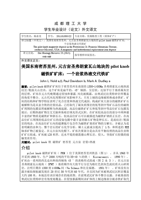
4 - 甲基-2 - 吡啶基 - 嘧啶铜(I)配合物的环反转引起的异构化引起的双发射摘要:我们开发了一种新的可换亞铜( I)使用2 - 吡啶基-4 - 甲基嘧啶和双膦作为配体。
这体现在复杂的机械双稳态的基础上,通过嘧啶环的反转运动,从而导致双LUMINES - cenc行为。
反转动力学强烈依赖于温度和溶剂。
环反转在溶液中相互转化,并且运动被冻结在200 K的复杂环境中,表现出特征性的CT吸收和发射带。
发光寿命的测量表明,该发射可以被卷积成两个部分。
快速和慢速分量被分配到两种异构体,激发态的特点是拥有不同的结构弛豫过程和/或额外的溶剂配位性能。
两种异构体不仅仅在发射特性的寿命和波长上不同,而且在热敏感性上不同。
两种异构体的摩尔比变化与溶剂的极性以及通过与阴离子的静电相互作用的抗衡有关。
反演的利率受溶剂影响,暗示反演由溶剂协调促进。
过渡金属配合物照片处理引起人们感兴趣是因他们在染料敏化,太阳能电池,light 发光的设备的潜在使用上,与光触媒3D 对高热量的组合稳定、可逆的氧化还原活动、激烈的可见吸收,和长寿命电荷转移 (CT) 形成激发态。
最近,照片功能分子被综合了使用简单陈列作为双重磷光的金属配合物,存在两个独立的准备状态,有选择性地准备两种状态之一的方法到目前为止一直有限。
状态选择一个特点是通过一种可逆化学定义明确双稳态的过程。
最近,我们描述新的分子机械系统通过利用反演运动运作的电子门嘧啶对铜给内部( I- )或外部( O-)异构体研究,这对嘧啶的取代基是分别近端或远端的铜。
目前的工作,我们开发一个用 4 - 甲基-2 - (2'-吡啶基)嘧啶新的铜( I)配合物( Mepypm )和双[2 - (二苯基膦基)苯基]醚( DPEphos )作为配体。
这种复杂的几何表现出双稳态基于嘧啶,导致双发光的反转行为。
反转的动力是对温度敏感和溶剂,利用反演过程。
表明激发过程可以被调整。
图1。
环反演平衡之间i-和o-异构体的(1•BF4•CHCl3) ORTEP 视图,显示50%的概率取代-发了椭球。
具有吖嗪类化合物的有机光感受器[发明专利]
![具有吖嗪类化合物的有机光感受器[发明专利]](https://img.taocdn.com/s3/m/a223e8228bd63186bdebbccb.png)
专利名称:具有吖嗪类化合物的有机光感受器
专利类型:发明专利
发明人:纽斯雷拉·朱布兰,兹比格纽·托卡斯基,卡姆·W·劳申请号:CN200410043026.0
申请日:20040430
公开号:CN1573577A
公开日:
20050202
专利内容由知识产权出版社提供
摘要:改进的有机光感受器,包括导电基底以及所述导电基底上的光电导元件,所述光电导元件包括:(a)具有如右通式的电荷传输材料,其中,R包括氢原子、烷基、链烯基、杂环基或芳香基;X 包括芳基氨基;Y包括至少具有加溶取代基的9-亚芴基;以及(b)电荷产生化合物。
本发明还描述了相应的电子照相装置以及成像方法。
申请人:三星电子株式会社
地址:韩国京畿道
国籍:KR
代理机构:北京市柳沈律师事务所
更多信息请下载全文后查看。
Spin galvanic effect2002C
gradient,d f/d z,across the condensate.Such a gradient may be imprinted by a condensate velocity,because d f=d z¼mv= h,where m is the atomic mass.If N s is identified with f/p,the model predicts N s/v,in agreement with the observed v-dependent part of N s. Furthermore,for the largest v and for parameters consistent with the experiment,the model gives N s<15,in rough agreement with observation.For a soliton with a¼23a o,the calculated maximum number of atoms that ensures stability is only,6,000per soliton11,13,which accounts for far fewer atoms than the number contained in the initial repulsive condensate.Apparently,most of the atoms from the collapsing condensate are lost,while only a small fraction remain as solitons.Immediately after switching a from positive to negative,we observe a diffuse background of atoms spreading out axially.This observation is reminiscent of the jet emitted by a85Rb condensate after switching from repulsive to attractive interactions5.In our system,which is in the quasi-1D regime,the remnant atoms form solitons with atom number near their stability limit.The remarkable similarities between bright matter-wave solitons and optical solitons infibres26emphasize the intimate connection between atom optics with Bose–Einstein condensates27and light optics.Many issues remain to be addressed,however,including the dynamical process of soliton formation.In addition,further investigation of soliton interactions and collisions could be under-taken with this system.Finally,we speculate that an‘atomic soliton laser’,based on bright matter-wave solitons,may prove useful for precision measurement applications,such as atom interfero-metry28.A Received19March;accepted18April2002.Published online1May2002,DOI10.1038/nature747.1.Ruprecht,P.A.,Holland,M.J.,Burnett,K.&Edwards,M.Time-dependent solution of the nonlinearSchrodinger equation for Bose-condensed trapped neutral atoms.Phys.Rev.A51,4704–4711(1995).2.Bradley,C.C.,Sackett,C.A.&Hulet,R.G.Bose-Einstein condensation of lithium:observation oflimited condensate number.Phys.Rev.Lett.78,985–989(1997).3.Sackett,C.A.,Gerton,J.M.,Welling,M.&Hulet,R.G.Measurements of collective collapse in a Bose-Einstein condensate with attractive interactions.Phys.Rev.Lett.82,876–879(1999).4.Gerton,J.M.,Strekalov,D.,Prodan,I.&Hulet,R.G.Direct observation of growth and collapse of aBose–Einstein condensate with attractive interactions.Nature408,692–695(2000).5.Donley,E.A.et al.Dynamics of collapsing and exploding Bose–Einstein condensates.Nature412,295–299(2001).6.Stegeman,G.I.&Segev,M.Optical spatial solitons and their interactions:Universality and diversity.Science286,1518–1523(1999).7.Dalfovo,F.,Giorgini,S.,Pitaevskii,L.P.&Stringari,S.Theory of Bose-Einstein condensation intrapped gases.Rev.Mod.Phys.71,463–512(1999).8.Burger,S.,Bongs,K.,Dettmer,S.,Ertmer,W.&Sengstock,K.Dark solitons in Bose-Einsteincondensates.Phys.Rev.Lett.83,5198–5201(1999).9.Denschlag,J.et al.Generating solitons by phase engineering of a Bose-Einstein condensate.Science287,97–100(2000).10.Anderson,B.P.et al.Watching dark solitons decay into vortex rings in a Bose-Einstein condensate.Phys.Rev.Lett.86,2926–2929(2001).11.Pe´rez-Garcı´a,V.,Michinel,H.&Herrero,H.Bose-Einstein solitons in highly asymmetric traps.Phys.Rev.A57,3837–3842(1998).12.Muryshev,A.E.,van Linden van den Heuvell,H.B.&Shlyapnikov,G.V.Stability of standing matterwaves in a trap.Phys.Rev.A60,R2665–R2668(1999).13.Carr,L.D.,Leung,M.A.&Reinhardt,W.P.Dynamics of the Bose-Einstein condensate:quasi-one-dimension and beyond.J.Phys.B33,3983–4001(2000).14.Kivshar,Y.S.,Alexander,T.J.&Turitsyn,S.K.Nonlinear modes of a macroscopic quantum oscillator.Phys.Lett.A278,225–230(2001).15.Schreck,F.et al.Quasipure Bose-Einstein condensate immersed in a Fermi sea.Phys.Rev.Lett.87,080403-1–080403-4(2001).16.Go¨rlitz,A.et al.Realization of Bose-Einstein condensates in lower dimensions.Phys.Rev.Lett.87,130402-1–130402-4(2001).17.Truscott,A.G.,Strecker,K.E.,McAlexander,W.I.,Partridge,G.B.&Hulet,R.G.Observation ofFermi pressure in a gas of trapped atoms.Science291,2570–2572(2001).18.McAlexander,W.I.Collisional Interactions in an Ultracold Lithium Gas.Thesis,Rice Univ.(2000).19.Tiesinga,E.,Verhaar,B.J.&Stoof,H.T.C.Threshold and resonance phenomena in ultracold ground-state collisions.Phys.Rev.A47,4114–4122(1993).20.Inouye,S.et al.Observation of Feshbach resonances in a Bose–Einstein condensate.Nature392,151–154(1998).21.Roberts,J.L.,Claussen,N.R.,Cornish,S.L.&Wieman,C.E.Magneticfield dependence of ultracoldcollisions near a Feshbach resonance.Phys.Rev.Lett.85,728–731(2000).22.Zakharov,V.E.&Shabat,A.B.Exact theory of two-dimensional self-focusing and one-dimensionalself-modulation of waves in nonlinear media.Sov.Phys.JETP34,62–65(1972).23.Carr,L.D.,Clark,C.W.&Reinhardt,W.P.Stationary solutions of the one-dimensional nonlinearSchro¨dinger equation.II.Case of attractive nonlinearity.Phys.Rev.A62,063611-1–063611-10(2000).24.Tai,K.,Hasegawa,A.&Tomita,A.Observation of modulational instability in opticalfibers.Phys.Rev.Lett.56,135–138(1986).25.Gordon,J.P.Interaction forces among solitons in opticalfibers.Opt.Lett.8,596–598(1983).26.Hasegawa,A.Optical Solitons in Fibers(Springer,New York,1990).27.Lenz,G.,Meystre,P.&Wright,E.M.Nonlinear atom optics.Phys.Rev.Lett.71,3271–3274(1993).28.Kasevich,M.A.Atom interferometry with Bose-Einstein condensed atoms.C.R.Acad.Sci.IV2,497–507(2001).AcknowledgementsWe thank W.I.McAlexander for providing the coupled channels calculation,B.Luey for making the magnetic coils,and T.Killian and H.Stoof for discussions.This work was supported by the US National Science Foundation,NASA,the Office of Naval Research and the Welch Foundation.Competing interests statementThe authors declare that they have no competingfinancial interests.Correspondence and requests for materials should be addressed to R.G.H.(e-mail:randy@). .............................................................. Spin-galvanic effectS.D.Ganichev*†,E.L.Ivchenko†,V.V.Bel’kov†,S.A.Tarasenko†, M.Sollinger*,D.Weiss*,W.Wegscheider*‡&W.Prettl**Fakulta¨t fu¨r Physik,Universita¨t Regensburg,D-93040Regensburg,Germany †A.F.Ioffe Physico-Technical Institute of the RAS,194021St Petersburg,Russia ‡Walter Schottky Institut,TU Mu¨nchen,85748Garching,Germany ............................................................................................................................................................................. There is much recent interest in exploiting the spin of conduction electrons in semiconductor heterostructures together with their charge to realize new device concepts1.Electrical currents are usually generated by electric or magneticfields,or by gradients of,for example,carrier concentration or temperature.The electron spin in a spin-polarized electron gas can,in principle, also drive an electrical current,even at room temperature,if some general symmetry requirements are met.Here we demon-strate such a‘spin-galvanic’effect in semiconductor heterostruc-tures,induced by a non-equilibrium,but uniform population of electron spins.The microscopic origin for this effect is that the two electronic sub-bands for spin-up and spin-down electrons are shifted in momentum space and,although the electron distribution in each sub-band is symmetric,there is an inherent asymmetry in the spin-flip scattering events between the two sub-bands.The resulting currentflow has been detected by applying a magneticfield to rotate an optically oriented non-equilibrium spin polarization in the direction of the sample plane.In contrast to previous experiments,where spin-polarized currents were driven by electricfields in semiconductor2,3,we have here the complementary situation where electron spins drive a current without the need of an external electricfield. Although it is usually ignored,it is well known that the spin degeneracy of sub-bands in semiconductor quantum well(QW) structures can be lifted,owing to terms linear in the wavevector k resulting from the spin orbit interaction in asymmetric potentials4,5. For a two-dimensional electron gas(2DEG)system,this leads to the situation sketched in Fig.1.The electron energy band splits into two sub-bands which are shifted in k-space and each of the bands comprise states with spin up or down.In this band structure spin polarization means that one sub-band is occupied up to higher energies than the other.This is depicted in Fig.1,illustrating that there are more spin-down than spin-up electrons.Can such a situation of uniform spin polarization cause an electric current? As long as the carrier distribution in each sub-band is symmetric around the sub-band minimum at k x^no currentflows.However, asymmetric k-dependent spin relaxation events can occur,indicatedby the dashed arrows in Fig.1,which result in a current flow.This means that a current is driven by a homogeneous spin polarization.Below we describe the observation of such a current.Phenomenologically,an electric current can be linked by general symmetry arguments to the electron’s averaged spin S byj a ¼gX Q ag S g ð1Þwhere j is an electric current density,Q is a second-rank pseudo-tensor,and a ,g ¼1,2indicate coordinates.Non-vanishing tensorcomponents Q ag can only exist in non-centrosymmetric systems belonging to one of the gyrotropic classes 6.In zinc-blende-based heterojunctions with a 2DEG,non-zero components of Q ag exist in contrast to the corresponding bulk crystals 7.In our (001)-grown heterojunctions with the C 2n symmetry only two linearly indepen-dent components,Q xy and Q yx ,are different from zero (x k [11¯0]and y k [110])where x and y are cartesian coordinates.Hence,to observe a spin-polarization-driven current a spin component lying in the plane of the heterojunctions is required (for example,S y in Fig.2).To achieve an in-plane spin orientation in experiment one could either use spin selective contacts 8(see Fig.2a)or optical orientation 9by using circularly polarized light.Although significant progress concerning electrical spin injecting has been made recently 10–12,reliable spin-injection into lateral low-dimensional electron sys-tems —at room temperature —is still a challenge.Furthermore,electrical spin injection causes,apart from the driving current,a laterally inhomogeneous spin polarization and hence additional driving forces for current flow which would hamper the unam-biguous demonstration of the effect described here.Instead,we use optical spin orientation,which ensures a homogeneous non-equili-brium spin polarization and directly proves the spin-galvanic effect.In this case of exciting electrons from the valence band to the conduction band the conduction band gets selectively spin-popu-lated owing to selection rules which allow transitions by circularly polarized light only if the spin of the electron is changed by ^1.In addition to this method we have also used circularly polarized terahertz radiation causing intraband instead of interband exci-tation.One interesting aspect of employing terahertz radiation isthat only one type of carriers,electrons or holes,is involved.In this respect,the effect of intraband spin orientation 13is indeed very close to electrical spin injection.It has been shown before that irradiation of quantum wells with circularly polarized light can result in a photocurrent caused by non-uniformly distributing photoexcited carriers in k -space according to optical selection rules and energy and momentum conservation.This is the circular photogalvanic effect observed recently in a 2DEG 14.In order to achieve a uniform distribution in spin sub-bands and to exclude this circular photogalvanic effect we use the geometry depicted in Fig.2b,where the photogalvanic current is identical to zero for normal incidence of the light 14.In this geometry,optical excitation yields a steady-state spin orientationS 0z in the z direction with the generation rate S˙z proportional to the intensity of the radiation.To obtain an in-plane component of the spins,necessary for the effect we describe here,a magnetic field,B ,was applied (Fig.2b).The field perpendicular to both the light-propagation direction eˆz and the optically oriented spins rotates the spins into the plane of the 2DEG owing to Larmor precession.With the magnetic field oriented along the x axis we obtain a non-equilibrium spin polarization S y which reads,after time averaging 7:S y ¼2q L t s ’1þðq L t s Þ2S 0zð2Þwhere t s ¼ffiffiffiffiffiffiffiffiffiffiffiffit s k t s ’p and t s k ,t s ’are the longitudinal and transverseelectron-spin-relaxation times,q L ¼g m B B x = his the Larmor fre-quency,g is the in-plane effective electron g -factor,m B is the Bohrmagneton,and S 0z ¼t s k _Sz is the steady-state electron spin polar-ization in the absence of the magnetic fiing the Larmor precession we prepared the situation sketched in Fig.1where the spin polarization S y lies in the plane.The denominator in equation (2)yielding the decay of S y for q L exceeding the inverse spin-relaxation time is well known from the Hanle effect 15.The experiments were carried out at room temperature (T ¼293K)and at liquid helium temperature on n -GaAs/AlGaAs single quantum wells of 15-nm width and on GaAs single hetero-junctions.The (001)-oriented samples grown by molecular beam epitaxy contain 2DEG systems with electron densities n s .2£1011cm 22and mobilities m above 106cm 2V 21s 21at T ¼4.2K.Two pairs of contacts were centred on opposite sample edgesalong the directions x k [11¯0]and y k [110](see inset in Fig.3).Complementary measurements were also carried out on p -GaAs multiple quantum-well structures containing 20wells of 15-nm width with hole densities in each well p s ¼2£1011cm 22and m ¼5£105cm 2V 21s 21:At room temperature a magnetic field of up to 1T was generated by an electromagnet.For the low-temperature measurements the samples were placed in a cryostat with a split-coil superconducting magnet yielding a field B of up to 3T.For optical interband excitation a continuous-wave Ti:sapphire laser was used at a wavelength of l ¼0.777m m.In order to extract the spin-galvanic current the linearly polarized laser beam was transmitted throughaFigure 1Microscopic origin of the spin-galvanic current in the presence of k -linear terms in the electron hamiltonian.The j y k x term in the hamiltonian splits the conduction band into two parabolas with the spin ^1=2in the y direction.If one spin sub-band ispreferentially occupied,for example,by spin injection (the ðj 21=2l y -states shown in the figure)asymmetric spin-flip scattering results in a current in the x direction.The rate of spin-flip scattering depends on the value of the initial and final k -vectors.There are four distinct spin-flip scattering events possible,indicated by the arrows.The transitions sketched by dashed arrows yield an asymmetric occupation of both sub-bands and hence a current flow.If,instead of the spin-down sub-band,the spin-up sub-band is preferentially occupied the current direction isreversed.Figure 2Two ways of generating an in-plane spin-polarization.a ,The spin injection from ferromagnetic contacts of magnetization M into the two-dimensional electron gas (2DEG).b ,The optical orientation in combination with an in-plane magnetic field B x .Spins,initially aligned along the z direction are rotated into the y direction by B x .photoelastic modulator which yields a periodically oscillating polarization between right-circular and left-circular.The current was recorded by a lock-in amplifier in phase with the modulator.For intraband excitation we used the l ¼148m m line of a pulsed ammonia laser 16.The current of unbiased samples was measured by the voltage drop on a 50Q load resistor in a closed circuit configuration.Both for visible and terahertz radiation a current has been observed for all n -type samples after applying an in-plane magnetic field (Figs 3and 4).For small magnetic fields B where q L t s ,1holds,the spin-galvanic current increases linearly as expected from equations (1)and (2).This is seen in the room-temperature data of Fig.3and in the 4.2K data in Fig.4for B #1T.The polarity of the current depends on the direction of the excited spins (^z -direction for right-or left-circularly polarized light,respectively)and on the direction of the applied magnetic field (^x direction).The current is parallel (or anti-parallel)to the magnetic field paring the power sensitivity for visible and terahertz excitation we find them to be of the same order of magnitude as seen in Fig.3.However,we note that the current contribution per photon is larger by two orders of magnitude for interband excitation.This is due to a more effective spin generation rate by interband excitation.It may even be larger,because the signal gets partially shortened by photogenerated carriers in the semi-insulating substrate.For higher magnetic fields the current saturates and decreases upon further increase of B ,as shown in Fig.4.This is ascribed to the Hanle effect,see equation (2).The observation of the Hanle effect demonstrates that free carrier intraband transitions can polarize the spins of electron systems.The measurements allow us to obtain the spin-relaxation time t s from the peak position of the photocurrent where q L t s ¼1holds if the g -factor is known.The g -factor of quantum wells,however,depends strongly on structural details.This leads to an uncertainty in the measured spin lifetime ing the theoretically estimated 17value of g ¼20.2results in t s ¼40ps at 4.2K.Spin-relaxation times of the same order of magnitude as derived here have been obtained by photolumines-cence measurements 18.However,direct comparison of these results with our data is difficult,because optical recombination does not detect the spin-relaxation time at the Fermi energy of the 2DEG,as in the present case of monopolar spin orientation.Published dataon Faraday rotation experiments,which give access to spin relax-ation at the Fermi level,however,refer to materials which are not directly comparable to our samples 19,20.Because the in-plane g -factor for heavy holes is very small 21,the associated spin-galvanic effect is expected to be negligible.Indeed no magnetic-field-induced current has been observed in p -GaAs quantum wells at terahertz excitation causing spin polarization of holes only.We note that a magnetic-field-induced circular photo-galvanic effect in p -type bulk materials was previously observed in GaAs at intraband excitation 22.However,this effect is not due to spin orientation and does not occur in p -type quantum wells owing to spatial quantization 23.Only for visible excitation,which polarizes both electrons and holes,has a current signal been detected in p -type samples (see Fig.3).This current is due to the spin polarization of electrons again,which are in this case the minority carriers generated by interband excitation.Microscopically,the spin-galvanic effect is caused by the asym-metric spin-flip relaxation of spin-polarized electrons in systems with k -linear contributions to the effective hamiltonian.The lifting of spin degeneracy of 2DEG depicted in Fig.1is a consequence of a contribution to the hamiltonian of the form ^H k ¼Pga b ag j a k gwhere j a are the Pauli spin matrices and b ag is a pseudo-tensor subjected to the same symmetry restriction as the pseudo-tensor Q ag used in equation (1).Figure 1sketches the electron energy spectrum with the b yx j y k x term included.Spin orientation in the y direction causes an unbalanced population in the spin-down and spin-up sub-bands.The current flow is caused by the k -dependent spin-flip relaxation processes.Spins oriented in the y direction are scattered along k x from the higher filled (for example,spin-down)sub-band,j 21/2l y ,to the less filled spin-up sub-band,j þ1/2l y .Four quantitatively different spin-flip scattering events exist and are sketched in Fig.1by bent arrows.The spin-flip scattering rate depends on the values of the wavevectors of the initial and the final states,respectively 24.Therefore spin-flip transitions,shown by solid arrows in Fig.4,have the same rates.They preserve the symmetric distribution of carriers in the sub-bands and,thus,do not yield a current.However,the two scattering processes shown by broken arrows are not equivalent and generate an asymmetric carrier distribution around the sub-band minima in both sub-bands.This asymmetric distribution results in a current flow along the x direction.Within our model of elastic scattering the current isnotFigure 3Current density j x normalized to the radiation power P as a function of the magnetic field B for normally incident circularly polarized radiation at room temperature for various samples and wavelengths.Filled symbols:l ¼0.777m m,P ¼100mW.Triangles,squares and circles correspond to n -type and p -type multiple quantum wells,and an n -type GaAs/AlGaAs heterojunction,respectively.Open squares:n -type GaAs/AlGaAs heterojunction,l ¼148m m,P ¼20kW.The inset shows the geometry of the experiment where e ˆz indicates the direction of the incoming light.Figure 4Current j x as a function of magnetic field B for normally incident right-handed (open circles)and left-handed (filled circles)circularly polarized radiation at l ¼148m m and radiation power 20kW.Measurements are presented for a n -GaAs/AlGaAs single heterojunction at T ¼4.2K.Curves are fitted from equation (2)using the same value of the spin relaxation time t s and scaling of the j x value for the solid curve as for the dashed curve.spin-polarized because the same number of spin-up and spin-down electrons move in the same direction with the same velocity.In the case of inelastic scattering the current may be polarized.The uniformity of the spin polarization in space is preserved during the scattering processes.Therefore,the spin-galvanic effect differs from surface currents induced by inhomogeneous spin orientation25.It also differs from other experiments where the spin current is caused by gradients of potentials,concentrations and so on,like the spin-voltaic effect26,27and the photo-voltaic effect,which occur in inhomogeneous samples,and like the‘para-magnetic metal-ferromagnet’junction or p-n junctions.When considering spintronic devices involving heterojunctions,spin-galvanic current must be taken into account.A Received3January;accepted25March2002.1.Wolf,S.A.et al.Spintronics:a spin-based electronics vision for the future.Science294,1488–1495(2001).2.Ha¨gele,D.et al.Spin transport in GaAs.Appl.Phys.Lett.73,1580–1582(1998).3.Kikkawa,J.M.&Awschalom,teral drag of spin coherence in gallium arsenide.Nature397,139–141(1999).4.Bychkov,Y.A.&Rashba,E.I.Properties of a2D electron gas with lifted spectral degeneracy.Sov.JETPLett.39,78–81(1984).5.D’yakonov,M.I.&Kocharovskii,V.Yu.Spin relaxation of two-dimensional electrons innoncentrosymmetric semiconductors.Sov.Phys.Semicond.20,110–111(1986).6.Koopmans,B.,Santos,P.V.&Cardona,M.Optical activity in seminconductors:stress andconfinement effects.Phys.Status Solidi205,419–463(1998).7.Ivchenko,E.L.,Lyanda-Geller,Yu,B.&Pikus,G.E.Current of thermalized spin-orientedphotocarriers.Sov.Phys.JETP71,550–557(1990).8.Fiederling,R.et al.Injection and detection of spin-polarized current in a light-emitting diode.Nature402,787–789(1999).9.Meier,F.&Zakharchenya,B.P.(eds)Optical Orientation1–523(Elsevier Science,Amsterdam,1984).10.Hammar,P.R.&Johnson,M.Spin-dependent current transmission across a ferromagnet-insulator-two-dimensional electron gas junction.Appl.Phys.Lett.79,2591–2593(2001).11.Zhu,H.J.et al.Room-temperature spin injection from Fe into GaAs.Phys.Rev.Lett.87,016601-1–016601-4(2001).12.Hanbicki,A.T.et al.Efficient electrical spin injection from a magnetic metal/tunnel barrier contactinto a semiconductor.Appl.Phys.Lett.80,1240–1242(2002).13.Tarasenko,S.A.&Ivchenko,E.L.Spin orientation of two-dimensional electron gas under intrabandoptical pumping.Preprint cond-mat/0202471at k l(2002).14.Ganichev,S.D.et al.Conversion of spin into direct electric current in quantum wells.Phys.Rev.Lett.86,4358–4361(2001).15.Hanle,W.U¨ber magnetische Beeinflussung der Polarisation der Resonanzfluoreszenz.Z.Phys.30,93–105(1924).16.Ganichev,S.D.Tunnel ionization of deep impurities in semiconductors induced by terahertz electricfields.Physica B273–274,737–742(1999).17.Ivchenko,E.L.,Kiselev,A.A.&Willander,M.Electronic g-factor in biased quantum wells.Solid StateCommun.102,375–378(1997).18.Damen,T.C.et al.Subpicosecond spin relaxation dynamics of excitons and free carriers in GaAsquantum wells.Phys.Rev.Lett.67,3432–3435(1991).19.Kikkawa,J.M.et al.Room-temperature spin memory in two-dimensional electron gases.Science277,1284–1287(1997).20.Sandu,J.S.et al.Gateable suppression of spin relaxation in semiconductors.Phys.Rev.Lett.86,2150–2153(2001).21.Marie,X.et al.Hole spin quantum beats in quantum-well structures.Phys.Rev.Lett.60,5811–5817(1999).22.Andrianov,A.V.&Yaroshetskii,I.D.Magnetic-field-induced circular photovoltaic effect insemiconductors.Sov.JETP Lett.40,882–884(1984).23.Ivchenko,E.L.,Lyanda-Geller,Yu,B.&Pikus,G.E.Circular magnetophotocurrent and spin splittingof band states in optically-inactive crystals.Solid State Commun.69,663–665(1989).24.Averkiev,N.S.,Golub,L.E.&Willander,M.Spin relaxation anisotropy in two-dimensionalsemiconductor systems.Preprint cond-mat/0202437at k l(2002).25.Averkiev,N.S.&D’yakonov,M.I.Current due to inhomogeneity of the spin orientation of electronsin a semiconductor.Sov.Phys.Semicond.17,393–395(1983).26.Johnson,M.&Silsbee,R.H.Interfacial charge-spin coupling:injection and detection of spinmagnetization in metals.Phys.Rev.Lett.55,1790–1793(1985).27.Zutic,I.,Fabian,J.&Das Sarma,S.Spin-polarized transport in inhomogeneous magneticsemiconductors:theory of magnetic/nonmagnetic p–n junctions.Phys.Rev.Lett.88,066603-1–066603-4(2001).AcknowledgementsWe thank D.I.Kovalev,W.Schoepe and M.Bichler for helpful discussions and support. We acknowledgefinancial support from the DFG,the RFFI and INTAS.Competing interests statementThe authors declare that they have no competingfinancial interests.Correspondence and requests for materials should be addressed to S.D.G.(e-mail:sergey.ganichev@physik.uni-regensburg.de)............................................................... Terahertz semiconductor-heterostructure laserRu¨deger Ko¨hler*,Alessandro Tredicucci*,Fabio Beltram*,Harvey E.Beere†,Edmund H.Linfield†,A.Giles Davies†,David A.Ritchie†,Rita C.Iotti‡&Fausto Rossi‡*NEST-INFM and Scuola Normale Superiore,Piazza dei Cavalieri7,56126Pisa, Italy†Cavendish Laboratory,University of Cambridge,Madingley Road,Cambridge CB30HE,UK‡INFM and Dipartimento di Fisica,Politecnico di Torino,Corso Duca degli Abruzzi24,10129Torino,Italy ............................................................................................................................................................................. Semiconductor devices have become indispensable for generat-ing electromagnetic radiation in everyday applications.Visible and infrared diode lasers are at the core of information technol-ogy,and at the other end of the spectrum,microwave and radio-frequency emitters enable wireless communications.But the terahertz region(1–10THz;1THz51012Hz)between these ranges has remained largely underdeveloped,despite the identi-fication of various possible applications—for example,chemical detection,astronomy and medical imaging1–4.Progress in this area has been hampered by the lack of compact,low-consump-tion,solid-state terahertz sources5–9.Here we report a monolithic terahertz injection laser that is based on interminiband tran-sitions in the conduction band of a semiconductor(GaAs/ AlGaAs)heterostructure.The prototype demonstrated emits a single mode at4.4THz,and already shows high output powers of more than2mW with low threshold current densities of about a few hundred A cm22up to50K.These results are very promising for extending the present laser concept to continuous-wave and high-temperature operation,which would lead to implemen-tation in practical photonic systems.In conventional semiconductor lasers,light is generated by the radiative recombination of conduction band electrons with valence band holes across the bandgap of the active material;in contrast, electrons in a quantum-cascade laser propagate through a potential staircase of coupled quantum wells,where the conduction band is split by quantum confinement into a number of distinct sub-bands10.By choice of layer thickness and applied electricfield, lifetimes and tunnelling probabilities of each level are engineered in order to obtain population inversion between two sub-bands in a series of identical repeat units.Injector/collector structures connect these active regions,allowing electrical transport through injection of carriers into the upper laser level,and extraction of carriers from the lower laser level.The radiation frequency is determined by the energy spacing of the lasing sub-bands,allowing in principle operation at arbitrarily long wavelengths.The quantum-cascade scheme has thus long been the preferred choice in many attempts to fabricate a terahertz semiconductor laser.Although electrolumines-cent devices have been reported by several groups11–14,laser action has been shown only at much shorter wavelengths15,16.In fact,above the forbidden phonon band of the material,direct electron–longi-tudinal optical(LO)phonon scattering processes can be con-veniently used to achieve large population inversions16. Furthermore,an additional problematic issue for the terahertz range stems from the fact that conventional laser waveguides are not suitable,owing to large free-carrier absorption losses and practical limitations on the thickness of epilayer growth.As in all lasers,efficient depletion of the lower level is essential, and long lifetimes of the upper level are highly desirable.Up until now,proposed terahertz quantum-cascade designs focused mainly on the latter aspect.To this end,structures have featured narrow injector minibands to both suppress scattering of electrons from the。
【doc】高能所2002年发表的专著及在学术刊物上公开发表的论文
高能所2002年发表的专著及在学术刊物上公开发表的论文附录3.发表论文目录141附录3.高能所2002年发表的专着及在学术刊物上公开发表的论文作者(以原序发表干U物名称序号专着或论文题目单位排列)卷号(年)页lFirstMeasurementofthe实验物理J.Z.Baieta1.Phys.Rev. BranchingFractionoftheDecay中心BESCollab.D65(2002)052004v/(2s,Z-+一2MeasurementoftheCrOSSSection实验物理J.Z.Baieta1.Phys.Rev.Lett.f0ree一hadronsat中心BESCollab.88(2002)101802Center-of-massEnergiesfrom2to5GeV3AMeasurementof(2)实验物理J.Z.Baicta1.Phys.Lett.中心BESCollab.B550(2002)24?32ResonanceParamcters4/.3(z7/"一)分支比实验物理BES合作组高能物理与核物理中心26(2002)8?16的测定5Decaysofthe/to∑..实验物理BES合作组高能物理与核物理FinalState中心26(2002)93?996中性和带电D介子单举半轻子实验物理BES合作组高能物理与核物理(电子)衰变分支比的测量中心26(2002)547?5567D和D.介子的遍举实验物理BES合作组高能物理与核物理分支比上限的测定中心26(2002)1093?11028北京谱仪II中性径迹测量误差的实验物理王君等高能物理与核物理确定中心26(2002)116-1219用联合D.和D单双标记测定实验物理荣刚等高能物理与核物理分支比的方法中心26(2002)207-215l0TEX0N0低能中微子实验中的实验物理李金等高能物理与核物理CsI(T1)晶体探测器中心26(2002)393-401l1TELESIS在3y衰变末态实验物理许国发等高能物理与核物理分析中的应用中心26(2002)462?470l2TEX0N0中微子实验屏蔽效果实验物理陈栋梁等高能物理与核物理的MonteCarlo研究中心26(2002)626?631l3在BEPCII/BESIII上寻找r/和实验物理李刚等高能物理与核物理中心26(2002)645-651态的MonteCar1o研究l4EnergyCalibrationofCsI(TI)实验物理岳骞等高能物理与核物理CrystalforQuenchingFactor中心26(2002)728?734 MeasurementinDarkMatterSearchl5最优化的北京谱仪取数时间实验物理苑长征等高能物理与核物理中心26(2002)759?765l42中国科学院高能物理研究所2002年《年报》豁幸●}案}謦謦沓尊l_专蓝l霉1'奄譬,鼍善童警{孳鼍上{点《l,作者(以原序发表刊物名称序号专着或论文题目单位排列)卷号(年)页l6MeasurementofQuenchingFactor实验物理岳骞等高能物理与核物理forNuclearRecoilsinCsI(TI)中心26(2002)855—860Crystall7北京谱仪(BESII)的飞行时间计实验物理彭海平等高能物理与核物理数器(1_0F)蒙特卡罗模拟的改进中心26(2002)86l一869l8TEXONO反应堆中微子能谱的实验物理陈栋梁,李金等高能物理与核物理计算中心26(2002)889—894l9R值测量中束流相关本底的扣除实验物理鄢文标等高能物理与核物理方法中心26(2002)998—100320北京谱仪(BESII)的飞行时间计实验物理彭海平等高能物理与核物理数器(TOF)时间和分辨律的修中心26(2002)1078-1086正2lt粲能区物理及对加速器和探测实验物理苑长征等高能物理与核物理器设计的要求中心26(2002)1201—120822BES--III主漂移室输出信号的模实验物理王铮等高能物理与核物理拟中心26(2002)1297—130123高速串行数据通信VME插件的实验物理章平等核电子学与探测技术研制中心22(2002)44—4624BESII快速数据重建实验物理荣刚等核电子学与探测技术中心22(2002)105—11025数字式随机脉冲产生器实验物理富洪玉等核电子学与探测技术中心22(2002)162—16526微阴极条感应室实验物理李金等核电子学与探测技术中心22(2002)193—19927BESIII系统环境的网络监测模型实验物理宋立温等核电子学与探测技术中心22(2002)272—27528CMS阴极条室的张力和丝距测实验物理姜春华等核电子学与探测技术量中心22(2002)335—33729北京谱仪PC机物理分析平台介实验物理刘天容等核电子学与探测技术绍中心22(2002)367—37030新型智能CAMAC机箱控制器实验物理张永吉,赵京伟核电子学与探测技术中心等22(2002)382—3843l基于DSP的多通道波形取样电实验物理王铮核电子学与探测技术路设计中心22(2002)409—41132~(3770)扫描实验中利用快速实验物理郭义庆等核电子学与探测技术重建数据测量数据样本的积分亮中心22(2002)420—423度33基于WEB的BES数据存储系统实验物理叶梅等核电子学与探测技术模型中心22(2002)449—45234StudiesofPrototypeCsI(TI)实验物理Y.Liu(刘延)etNIMA482(2002)125 CrystalScin—tillatorsforLow中心a1.EnergyNeutrinoExperiments鬟一附录3.发表论文目录143作者(以原序发表刊物名称序号专着或论文题目单位排列)卷号(年)页35NuclearRecoilMeasurementsin实验物理M.Z.Wang,Phys.Lett.CsI(TbCrystalforColdDark中,J.Li(李金)eta1.B536(2002)203Mat'terDetection36ProbingNeutrinoOscillation实验物理Y.F.Wang(王Phys.ReD65(2002)0730 jointlyinLongandveryLong中心贻芳)etal2lBaselineExperiments37OntheOptimumLongBaseline实验物理Y.F.Wang(王Phys.Rev.D65(2002)0730 f0rtheNextGenerationNeutrino中心贻芳)etaI.06OscillationExperiments38StudyonthePropertyoft天体物理G.M.ChenProceedingsofthethird HadronicDecays中心jointmeetingofChinesephyscistsworldwide,P.185,worldscientific200239Bs.dintechnicolormodel天体物理ZhaohuaPhys.Lett.B546(200)withscalars中心Xiong,JinMin22l-227Y ang40Loopeffectsandnondecoupling天体物理ZhaohuaXiongPhys.Rev.D66, propertyofsupersymmetricQCD中心et.a1.015007(2002)ingb--->tH.4lGreatScintillatingPropertiesofa天体物理GouQuanBuChin.Phys.Lett.V o1.19,Y ALO3:Cecrystal中心et.a1.No.7(2002)92942GreatScintillationgPropertiesofa天体物理苟全朴,李祖物理7期929.930Y A103:CeCrystal中心毫,吕雨生等43非重子暗物质粒子的研究进展天体物理盛祥东,何会物理9期31卷中心林.戴长江577-58044CirX.1的时变性质天体物理屈进禄等河北师大26,1,10中心月45致密星的X射线辐射时延现象天体物理屈进禄,宋黎天文学进展刊物20卷, 中心明,吴枚等第2期143.15546两类长Y暴的里叶功率谱天体物理申荣锋,宋黎明天文43卷第4期中心342-34547L3宇宙线实验触发系统和触发天体物理李忠朝,郁忠高能物理和核物理26. 效率的测量中心强,过雅南等172.17948~掏小型数据获取系统及天体物理何会林,戴长核电子学与探测技术CaF2(Eu)性能的测量中心江,盛祥东22卷第l期27.3049新型"CaF2(Eu)+液闪"复合天体物理盛祥东,戴长高能物理和核物理26 WIMP探测器的实验研究中心江,何会林卷3期273.27850Chandraobservationofsupernova天体物理E.J.Lu.TheAstrophysics568; remnantG54.1+0-3:Aclosecousin中心Q.D.Wang,L49.L52 oftheCRABnebulaL.M.Song,●,●,,,,f,},,};●,,,,,.}●I,I:}::I1,!1,tt●}t{,t,{.^I1.,'l_4l44中国科学院高能物理研究所2002年《年报》作者(以原序发表刊物名称序号专着或论文题目单位排列)卷号(年)页5lBlobejectionfrom天体物理Jian?Min,wangTheApjsadvection.dominatedaccretion中心dengl38:249.263flow.H.themultiwavelengthpropertiesoflightcurves52Comptelobservationsofthe天体物理S.ZhangdengAstronomy386,843?853 gamma-rayblazarpks1622?297中心53KilohertzQuasi—periodic天体物理Wenfei.YuTheAstrophysical osciliationfrequency中心deng567;L67-L70anticorrelatedwithmilihertzquasi—periodicoscillationfluxin4u1608.5254TheAccretionratesandspectral天体物理Jian?MinWangTheApjs energydistributionsofbllacetae中心dengobjects55Bs,d+?inTechnicolor天体物理ZhaohuaPhysicslettersb546 modelwithSCalarS中心Xiong,JinMin221.227Jang56Discoveryofa136millisecond天体物理F.J.LudengAstrophysics574:7卜74 radioandX?raypulsarin中心supernovaremnantG54.1+0.357Chandraobsevationofsupemova天体物理FJ.Lu.AstrophysicalremnantG54.1+0.3:aclosecousin中心L..M..song568;L-49一L52 ofthecrabnebula58低轨道空间闪烁探测器异常区开天体物理张承模,梁晓核电子学及探测技术关机设计及控制中心华,徐玉朋等第22卷第6期59Furtheranalysisofdi?gluonfusion理论室DongshengDu,HighEner.Phys.&Nuc1. mechanismforthedecaysofDeshanY angPhys.V.26,1(2002)B—T1'KandGuohuaiZhu60Phenomenologicalanalysisof理论室DongshengDu,Phys.Rev.D65,074001B--,PPdecayswithQCDHaijunGong,(2002)factorizationJunfengSunetal_6lPhenomenologicalanalysisof理论室DongshengDu,Phys.Rev.D65,094025 charmlessdecaysB—}PVwithHaUunGong,(2002),Erratum,ibid. QCDfactorizationJun~ngSunetD66,079904(2002)a1.62D—}7mdecayswithfinalstate理论室MedinaPhys.Lett.B536,34 interactionsAblikim,(2002)DongshengDu,MaozhiYang63CPasymmetryinx-sleptondecay理论室WeiminYang,Phys,Rev.D65,1I5005 intheminimalSUSYstandardDongshengDu(2002)model哮}謦j-1謦1.唾}..专簪■奄枣t鼍t.t蹙垂《l《'譬jj鼍t毒'1.●il-耄羹囊萋:附录3.发表论文目录145EIIEllI重IIIE|IlIEE宦E量III£EIIlIIIlIIIIIlEEIIIIEE譬EElEIElIIE氍EE群匿臀鐾鞋越匪匪暖壁E_曩EI-iiiI-重匿匪髭|曲B量E匡__譬I|l苍I重IIIIIIIII量lIEE,』作者(以原序发表干U物名称序号专着或论文题目单位排列)卷号(年)页64IsthetruncatedSU)理论室QishuY ah,Phys.Rev.D65,105009non-abeliangaugetheoryinextraDongshengDu(2002)dimensionsrenormalizable?65Branefluctuationandelectroweak理论室QishuY ah,Phys.Rev.D65,094034 chirallagrangianDongshengDu(2002)66Thesystematicstudyof理论室Zheng-TaoNuc1.Phys.BB7/"formfactorsinpQCDWei.Mao-Zhi642(2002)263 approachanditsreliabilityY ang67Calculationofpureannihilation理论室C.D.LuEuro.Phys.J.C24, typedecayB-yDsl2I-126(2002)68B一ⅡP.Ⅱ(I)Decaysin理论室C.D.LU.M.-Z.Euro.Phys.J.C23, PerturbativeQCDApproachY ang275-287(2002)69Constraintontheanglealphafrom理论室C.D.Ltt.z.-j.Phys.Rev.D66, theexperimentalmeasurementsofXiao074011(2002) directCPviolationofB0pipi—decay70Determiningthefactorization理论室Zhi-zhongXingHEP&NP26 parameterandstrongphase(2002)100differencesinB—Dzdecays7lFakeCPTviolationin理论室Zhi-zhongXingJ.Phys.G28 disappearanceneutrino(2002)7oscillations72TexturezerosandMajorana理论室Zhi-zhongXingPhys.Lett.B phasesoftheneutrinomassmatrix530(2002)15973Possibleimplicationsofsmallor理论室Zhi-zhongXingHEP&NP26 largeCPviolationinB—jKs(2002)197decays74RephasinginvariantsofCPandT理论室W.L.GUO.Phys.Rev.D violationinthefour-neutrinoZhi-zhongXing65(2002)073020 mixingmodels75Model-independentconstraintson理论室Zhi-zhongXingPhys.Rev.D65 theneutrinomassspectrumfrom(2002)077302theneutrinolessdoublebetadecay76Nearlytri-bimaximalneutrino理论室Zhi-zhongXingPhys.Lett.B mixingandCPviolation533(2002)8577Cantheleptonflavormixing理论室Zhi—zhongXingPhys.Rev.D matrixbesymmetric?65(2002)113010l46中国科学院高能物理研究所2002年《年报》作者(以原序发表刊物名称序号专着或论文题目单位排列)卷号(年)页78AfuIldeterminationofthe理论室Zhi-zhongXingPhys.LeR.B neutrinomassspectrumfrom539(2002)85two.zerotexturesoftheneutrinomassmatrix79Possibleeffectsof理论室Z.Chang,Phys.Rev.D66 noncommutativegeometryonZhi-zhongXing(2002)056009 weakCPviolationandunitaritytriangles80Apredictiveansatzforneutrino理论室Zhi-zhongXingPhys.Lett.B mixingandleptogenesis545(2002)3528lNoncommutativityofleptonmass理论室Zhi-zhongXingFortsch.Phys. matrices:flavormixingandCP50(2002)569violation82Hierarchicalneutrinomassesand理论室Zhi-zhongXingPhys.LeR.B largemixinganglesfromthe550(2002)l78 Fritzschtextureofleptonmassmatrices83Unitarityquadranglesoffour理论室W.L.Guo.Phys.Rev.D66neu~inomixingZhi-zhongXing(2002)09730284Poynt!ngVector,EnergyDensity理论室C.-G.Huang,'Phys.Rev.A65 andEnergyV elocityinAnomalousY.Z.Zhang(2002),015802DispersionMedium85ThermodynamicsofdeSitter理论室C.GHuang.Phys.Rev.DuniverseL.Liu,Bobo65(2002),.08350lWang86Negativegroupvelocityand理论室Chao-GuangJ.Optics.A: distortionofpulseinanomalousHuang,PureApp1.Optics.dispersivemediumYuan-ZhongZhang4(2002),263.87Thermodynamicsof理论室Bo-boWang,Class.Quant.Reissner-NordstromblackholesinChao-GuangGray.19(2002),2491.Y ork'SFormalismHuang88Propagationofrectangularpulse理论室Chao-GuangCommun.Theor.Phys.38 inananomalousmediumHuang,(2002),224.Yuan-ZhongZhang89V acuumBlackHoleMass理论室mun.Theor.Phys.38 FormulaisaV anishingNoetherGUO,C.G.(2002),309ChargeHuang,K.Wu90topquarkspincorrelationatlinear理论室Z.H.Lin,Phys.Rev.D65. colliderswithanomalousHan,Huang,0l4008(2002)couplingsJ.X.Wang.X.Zhang,}◆F辱}tF孽.,..'薹髻茎董;耋一附录3.发表论文目录147作者(以原序发表刊物名称序号专着或论文题目单位排列)卷号(年)页9lStabilityoftheClassicalSolution理论室YinYu-dongHEP&NP,V26 ofGaugeTheoryHuangTao(2002)28-3492S~ongCouplingsofHeavy理论室Z.H.Li.Phys.Rev.D65 MesonstOaLightV ectorMesonsT.Huang,(2002)076005inQCDJ.Z.Sun.Z.H.Dai93MuonAnomalousMagneticinthe理论室T.Efeng,Commun.111eor. SupersymmetricModelswithandT.Huang,Phys.37(2002)179withoutRi【ght-handedNeutrinosX.Q.LietaI.94SIGMAMESON【NJ/PSI理论室WujunHuo,Phys.Rev.D65 DECAYSXinminZhang,(2002)097505TaoHuang95ImpactoftheSoft-Gluon理论室X.YWu.CPL19(2002)1596 ExchangesonB一>pipiDecaysZ.H.Li,J.Y.Cui,T.Huang96Re-examinedRadiativeDecay理论室Zuo-HongLi,JPhysicsG inLightConeQCDXiang-Y aoWu,28(2002)2583SumRuIeTaoHuang97NewapproachtOconstructingthe理论室Da-QingLiu,HighEnergyPhys.and opermoronthela~icefortheJi-MinWu.Nuc1.Phys.26(2002)222 calculationofglueballmassesYingChen98StudyonthebaryonstateX理论室ShenQixing,Commun.Theor.Phys., producedintheprocessYuHong,Li37(2002)pp189-192J/gP+X.P+PDemin99Onthemassrelationofameson理论室De-MinLi,ModemPhys.Lett., nonetHongYu.17(2002)163-169Qi-XingShenl00Themassrelationbetweenthe理论室De-MinLi,ModemPhys.Lett., pureandphysicalgroundHongYu,17(2002)619-626 pseudoscalarglueballsQi-XingShenl0lNumericalcalculationofenergies理论室BinDUan,Eur,Phys.J.D ofsomeexcitedstatesinaXiao-Y ahGu,19(2002)9-12heliumatomZhong-QiMalO2Non.relativisticLevinson's理论室Shi—HaiDong,Phys.Rev.A65(2002) theoreminSD$dimensionsZhong-QiMa042717(1-6)l03Thehiddensymmetryfora理论室Shi-HaiDong,Am.J.Phys.70 quantumsystemwithaninfinitelyZhong-QiMa(2002)520-52I deepsquare?wellpotentiall04The(2+1)Diracequationwiththe理论室Shi-HaiDong,Found.Phys.Lett. deltapotentialZhong-QiMa15(2002)171-178●●●{'j●●f},,,!l{;.'+.}_.,},●.,●t,t}々jl48中国科学院高能物理研究所2002年《年报》蝣1簟毒Ili手睾每叁鸯夸誊;;:'一作者(以原序发表刊物名称序号专着或论文题目单位排列)卷号(年)页l05Quantumthree-bodysysteminD理论室Xiao-Y anGu,J.Math.Phys.43(2002) dimensionsBinDuan,2895-2906Zhong-QiMal06Algebraicapproachtothe理论室Shi-HaiDong,Inter.J.Mod,Phys.E11 pseudoharmonicoscillatorin2DZhong-QiMa(2002)155-160l07ExactsolutionstotheDirac理论室Xiao-Y anGu,Inter,J.Mod.Phys.E11, equationforaCoulombpotentialZhong-QiMa,(2002)335-346inD+ldimensionsShi-HaiDongl08ExactsolutionstoD-dimensional理论室Lu-YaWang,Found.Phys.Lett. SchrodingerequationwithaXiao-Y anGu,15(2002)569-576 pseudoharmonicoscillatorZhong-QiMaeta1.l09ExactsolutionsoftheDirac理论室Shi-HaiDong,Inter,J.Mod.Phys. equationwithXiao-Y anGu,E11(2002)483-489 aCoulombplusscalarpotentialinZhong-QiMa2+ldimensionseta1.l10群论习题精解理论室马中骐着科学出版社(北京)2002年出版l1lStudyofthestructureof理论室R.G.Ping,Phys.Rev.D66,baryonsfromJ/—÷BBbardecaysH.C,Chiang,054020(2002) intheciuarkmodelB.S.ZOUl12TheoreticalformalismandMonte理论室W.H.Liang,J.Phys.G28,333(2002) CarlostudyofpartialwavePN.Shen.analysisforfPP∞J.X.Wang,etal,l13Partondistributionofproton理论室Y.J.Zhang,Phys.Lett.B528, inasimplestatisticalmodelB.S.Zou,228(2002)L,M.Y angl14Commentonprotonium理论室C.Amslereta1.,Phys.Rev.D66:058101, annihilationintopi0pi0atrestinB.S.ZOU2002aliquidHydrogentargetl15i=0.C=-1mesonsfrom理论室A.AnisovichetPhys,Lett.B542:19-28,l940-mevto24l0-meva1..B.S.Zou2002l16Combinedanalysisofmeson理论室A.mnisovichPhys.Lett.B542:8-18, channelswithi=1.C=-1frometa1..B.S.Zou2002l940-mevto2410一mevl17High-EnergyProton-Induced理论室C.GDuan.Chin,Phys.Lett. DimuonProductionfromNucleiH.M.Wang.19(2002)485GL.Lil18~(400-1200)物理本质的探讨理论室李龙,邹冰松,高能物理与核物理厉光烈26(2002)346l19p-ADrell-Y an过程中的核效应理论室乔秀梅,段春高能物理与核物理贵,厉光烈26(2002)1036.附录3.发表论文目录149作者(以原序发表刊物名称序号专着或论文题目单位排列)卷号(年)页l20AGB星演化过程中的核合成理论室厉光烈,张妙静原子核物理评论和张波19(2002)301l2lATwoStepMechanismfor理论室YWYu.PHighEnergyPhys.and FormingDibaryonWang.Z.YNuc1.Phys.26(2002)46(f2f2):O+Zhangeta1.l22Multi-s~angeHypernucleiina理论室P.Wang.HNuc1.Phys.ChiralSU(3)QuarkMeanFieldGuO.Z.YA705(2o02)455 ModelZhangeta1.l23ChiralSymmetryRestorationof理论室EWang,H.J.Phys.G28(2002)2265 NuclearMatterGuO.YB.Dong.Z.YZhangYu124AnAnalysisofQuarkEffectin理论室Z.YZhang.HighEnergyPlays.and TwoBaryonSystemYuNuc1.Phys.26(2002)712125Di..mega(f2f2):0+理论室YWYu.EPhys.Rev.Wang.Z.YC66(2002)015205PriductionCrossSectionZhangeta1.Calculationl26D.NBoundStateinSU(3)Quark理论室YuZ.HighEnergyPhys.and ModelZhang,Q.B.LiNuc1.Phys.26(2002)1041l27Baryon+Baryon理论室YuCommen.Theo~Phys.cross(QQ):0+37(2002)443SectionCalculation128f)f20+DibaryonProducti.ns理论室mun.Theor.Phys.Wang.YWYu38(2002)483inCentralAu+AuCollisionsatRHICEnergy=130GeV129Dynamicalsymmetrybreaking,理论室Z.GWang.S.L.Phys.Lett. confinementwithflat-bottomWanB536(2002)24lPotentiall30Calculationofsomepropertiesof理论室Z.GWangJ.Phys.GNuc1.Part. thevaccuumPhys.28(2002)1l3lMassiveQuarkPropagatorinthe理论室M.Huang,ChinesePhys.Lett.COlO卜supercOnductingPhaseEEZhuang,19(2002)644W.Q.Chaol32AnalyticSolutionofGroundState理论室ZhaoWeiqin,HEP&NP26(2002)299 forCoulombPlusLinearPotentialJuChangsheng,.,口::i-,■■,;,■r■!:,l::;.tt;I:l50中国科学院高能物理研究所2002年《年报》作者(以原序发表千IJ物名称序号专着或论文题目单位排列)卷号(年)页l33MesonEff~ctsonChiral理论室HuangMei,Commun.Theor.Phys. CondensateatFiniteDensityZhuang38(2002)181Peng~i,ChaoWeiqinl34V ariationa1.IterativeSolutionof理论室ZhaoWeiqinCommun.Theor.Phys. GroundStateforCentralPotential38(2002)15l35DifferentV ersionsofPerturbative理论室ZhaoWeiqin,Commun.TheoEPhys. ExpansionBasedontheJuChangsheng38(2002)271Sin?。
- 1、下载文档前请自行甄别文档内容的完整性,平台不提供额外的编辑、内容补充、找答案等附加服务。
- 2、"仅部分预览"的文档,不可在线预览部分如存在完整性等问题,可反馈申请退款(可完整预览的文档不适用该条件!)。
- 3、如文档侵犯您的权益,请联系客服反馈,我们会尽快为您处理(人工客服工作时间:9:00-18:30)。
Vacuum 64(2002)315–319Cylindrical hollow magnetron cathode.Al–Nselective coatingsfor solar collector absorbersP.R.Gordo*,J.M.C.Cabac o,Yuri Nunes,V.M.B.Paix *ao,M.J.P.Maneira CEFITEC,Departimento de F !ısica,‘‘Campus ’’da FCT/UNL,2825Monte de Caparica,PortugalAbstractHollow magnetron cathodes are particularly useful in coating parts with cylindrical symmetry and when depositionmust be centripetal;this is the case when coating the outside of tubular and long substrates.A hollow magnetron cathode and its vacuum system has been designed and constructed to coat 2m long heat pipe absorbers and fluid pipe absorber tubes with a selective film of aluminum nitride.The pipe absorbers will be used in vacuum and non-vacuum compound parabolic concentrators (CPC)of different models for thermal solar collectors.The long copper substrates are displaced through the DC reactive glow discharge inside the hollow cathode.Coating occurs in a single run.Adequate values of discharge voltage and pressure were chosen and the relative nitrogen dose was optimized to get maximum absorbance of the film in the solar spectrum for several substrates.Reflectivities of less than 1%at the wavelength of 550nm and excellent adhesion were obtained.In these last tests the pull method has been used.r 2002Elsevier Science Ltd.All rights reserved.1.IntroductionSolar energy absorbing coatings are very im-portant as the main functional system in solar energy absorbers [1].Both good absorbance in the solar spectrum and low emissivity in the infrared zone are necessary to make a good selective coating.Magnetron sputtering [2,3]is being used to produce both the reflective and absorber coat-ings.This method has several advantages.It is a dry process which avoids future degassing in the vacuum collector tubes,it is almost pollution free,contrasts with the cases of the electrochemical methods that produce hazardous chemicals and paintings that produce aerosols.One additional advantage is the good adhesion inherent to the sputter coating processes.Aluminum nitride hasbeen recently used as the outer layer in a three-layer coating for glass absorber tubes for solar energy [1].Reactive magnetron discharge studies concerning aluminum nitride [4,5]and other nitrides [6,7]have been reported.In this paper it is shown that hollow magnetron cathodes can be particularly useful for coating parts with cylind-rical symmetry and when deposition must be centripetal,which is the case of the outside coating of tubular and long substrates.The pipe absorbers will be used in several models of vacuum and non-vacuum compound parabolic concentrators (CPC)[8].2.The coating apparatusThe apparatus consists of sample departure and sample arrival chambers linked by a hollow*Corresponding author.0042-207X/02/$-see front matter r 2002Elsevier Science Ltd.All rights reserved.PII:S 0042-207X (01)00294-9magnetron cathode,a pumping system and a gas inlet configuration,as shown in Fig.1.The sample departure and arrival chambers are about 2m long.The vacuum is supplied by turbomolecular and rotary pumps delivering a pumping speed about 500l/s.Pressure values refer to Pirani and Penning gauges,TPG 300from Balzers,calibrated for air.A pressure of 5Â10À4Pa can be obtained in about 5h.The gas inlet systems for nitrogen and argon are independent and both consist of a bottle regulator and a micrometric needle valve,allowing very fine control in the case of nitrogen.A gate valve ahead of the turbo pump provides throttling.The cylindrical aluminum wall of the hollow cathode has 10cm diameter and about 20cm length (see Fig.2).The targets are cylindrical and are put in place by tight sliding through the cathode inside.The magnetic field is provided by an external ring of Alnico horseshoe magnets laying directly over the cathode wall and encapsulated in a Ertalon box,allowing magnet and cathode cooling.The magnetic field is completely balanced [9],with the usual half-thoroidal configuration and an induc-tion value of 0.5T over the poles.A Huttinger DC power supply model PFG10000powers the cath-ode during the discharge.The long copper substrates or the multi-sample holder,are pushed by an outside motor driven mechanical system,through the center of the DC reactive glow discharge being coated in one run.3.Experimental procedureAfter purging with argon and nitrogen,the cleaning initial pressure is set as 2Â10À3Pa.Nitrogen and argon are successively admitted through metering valves and the respective pres-sure increments contribute to set the pressure in the vacuum chamber.The ratio of the nitrogen to argon pressure increments corresponds to theratioFig.1.Schematic diagram of theapparatus.Fig.2.Longitudinal schematic section of hollow magnetron cathode.The Alnico magnets are water-cooled and the insulators are made of Ertalon.P.R.Gordo et al./Vacuum 64(2002)315–319316of partial pressures and range from 0.05to 0.35.These ratios are used to express in arbitrary units the nitrogen dose relative to argon,henceforth called the nitrogen dose.The discharge pressure is set by throttling and was chosen to be 0.8Pa.During deposition all the substrates are located approximately in the center of the cathode at a distance of about 4–4.5cm from the target.Samples are organized in groups of 3,mounted nearby.One sample in each group is copper roughened by a glass sphere jet,the other is polished aluminum and the last one is a glass lamella.After setting the reactive discharge para-meters,the power supply is operated at constant voltage and at each nitrogen dose two groups of samples are coated.One group is located at the center of the plasma ring and the samples are referred as centered.Other group is located 4cm away of the center on the chamber axis and the samples are referred as edge samples (see Fig.3).Studies were carried out at three voltages,340,370and 400V.At each nitrogen dose and voltage,current and power were recorded.Deposition time is three minutes,which is enough in all cases,to guarantee opacity,verified with glass substrates.4.Results and discussionIn Fig.4,the current I v(d )at fixed voltage,V ,is shown and it is plotted against the nitrogen dose,d ,in arbitrary units as previously defined.One can observe that after an initial current flat zone,where Al–Nformed on the target is immediately sputtered [5,6],a current increase occurs for all voltages.This can correspond to the start of Al–N accumulation on the target and an eventual progressive change in the secondary emission coefficient,which would lead to an increase of the electron production yield on the target.As the nitrogen dose increases further between 0.13andFig.3.Longitudinal scheme of the hollow cathode showing the substratesposition.0.2,local minima for the 340and 370V curves and a plateau at 400V curve can be observed.One possible explanation would be a partial isolation of plasma electrodes by ‘‘poisoning’’with Al–N corresponding to an increase of the impedance in the discharge.At even higher nitrogen doses,the glow discharge starts to be unstable and tends to extinction.For each point of Fig.4,six samples were obtained,corresponding to three centered and three edge samples.The specular reflectivity at a 51incidence angle was measured for all the samples in a Shimadzu UV-2101PC spectrophotometer,using the standard reference calibrator.In the graphic of Fig.5,we show the variation of the sample’s reflectivity for the wavelength 550nm,as a function of the nitrogen dose for the three different centered substrates.These results corre-spond to 340V curve,in Fig.4.In Fig.5,two relatively flat zones appear at the lower and higher nitrogen dose values,separated by a sudden drop between nitrogen doses 0.13and 0.2where the reflectivity drops clearly under 1%for all sub-strates.Between the same nitrogen doses,in Fig.4,there is a plateau or even a local minimum in the current,already referred to,and that seems to correlate with the reflectivity well.Adhesion tests were performed by the pull method using a Sebastian Five (Quad Group)‘‘peel and pull’’tester.Epoxy adhesive was used on 0.37mm diameter aluminum pull studs of refer-ence PN901141C (Quad Group).Adhesive failure in the film–substrate interface was studied at the nitrogen dose 0.2with centered and edge samples.Results are summarized in Table 1,where max-imum stresses before failure in MPa,are presented in the studied cases.From the analysis of the table we conclude that adhesion is better by about a factor of two to three in the case of films growing as edge samples.Moreover the adhesive failure in these cases revealed that the bottom of the film is reflective,suggesting that the film grows initially rich in aluminum.On the contrary in the cases concerning coatings produced as centered samples,the adhe-sion is lower and the bottom part of the film is non-reflective,indicating that it is poor in alumi-num since the beginning of the growth.It is not clear why initially there is aluminum growthinFig.5.Semi-logarithmic plot of reflectivity,R ,for the wavelength 550nm,as a function of the nitrogen dose.The substrates are glass,aluminum and copper,centered samples.Table 1Maximum failure stress in MPa Substrate Edge samples Centered samples Copper 6.68 1.91Glass1.96 1.11Aluminum0.490.18P.R.Gordo et al./Vacuum 64(2002)315–319318edge samples and not in centered ones,however it seems that the initial aluminumfilm contributes as adhesion promoter between substrates and Al–N films.For doses at the left of the reflectivity well,the film has a dark blue color that turns to matte black in the well and becomes vitreous black in the higher dose zone.Normally Al–Nfilms obtained by molecular beam epitaxy(MBE),chemical vapor deposition(CVD)and reactive magnetron sputtering in low-pressure regimes are transparent with reflectivities of about10%in the visible spectrum[10,11].Heat pipe copper tubes were coated with Al–Nfilms and less than1% reflectivity at a51incidence was obtained,with a nitrogen dose of0.17.The cathode was DC operated up to400V and an approximate power of2200W.The speed of the traveling through the plasma necessary to get opacity is10cm per minute with this single plasma ring hollow cathode.5.ConclusionsIn this work a homemade hollow magnetron cathode was operated in the DC reactive mode to produce Al–Nthinfilms on copper heat pipe tubes.Current to nitrogen dose curves at constant voltage,and reflectivity dependence on nitrogen dose,were measured.An experimental correlation between the well in the reflectivity and the local minima in current as a function of the nitrogen dose is shown.Adhesion tests pointed out the difference of thinfilm properties when produced in the centered situation,showing the anisotropy of material deposition and the dependence of the mechanical properties on the geometry of the deposition.Further systematic studies to correlate plasma properties with reflectivity andfilm composition and structure are needed to a better understanding of the experimental results.This work permitted the optimization of the system and process parameters to obtain Al–Nthinfilms on copper heat pipe tubes with adequate adhesion and good reflectivity lower than1%.The setting of the manufacturing and equipment specifications for industrial production is now possible. References[1]Zhang Q-C,Zhao K,Zhang B-C,Wang L-F,Shen Z-L,Lu D-Q,Xie D-L,Zhou Z-J,Li B-J.J Vac Technol A 1998;16(2):628.[2]Thornton JA.J Vac Sci Technol1978;15(2):171.[3]Waits RK.J Vac Sci Technol1978;15(2):179.[4]McMahon R,Affinito J,Parsons RR.J Vac Sci Technol1982;20(3):376.[5]Affinito J,Parsons RR.J Vac Sci Technol A1984;2(3):1275.[6]Knotek O,Munz WD,Leyendecker T.J Vac Sci TechnolA1987;5(4):2163.[7]Este G,Westwood WD.J Vac Sci Technol A1987;5(4):1892.[8]Nunes CS,Mendes JF,Pereira MC,Maneira MP.Opticalmaterials technology for energy efficiency and solar energy conversion,vol.XIII.Bellingham,WA:SPIE,1994. [9]Jan-Eric Sundgreen F Nato AISI on diamond like thinfilms.Italy,July/August1990.[10]Dimitrova V,Manova D,Paskova T,Uzunov Tz,IvanovN,Dechev D.Vacuum1998;51:161.[11]Thompson MP,Drews AR,Huang C,Auner GW.MRSInternet J Nitride Semicond Res1999;4S1:G37.P.R.Gordo et al./Vacuum64(2002)315–319319。