AD9388ABSTZ-170中文资料
wm8978中文介绍说明资料doc资料

绪论.................................... 13 特征............................................................... 14 麦克风输入......................................................... 14 PGA 和 ALC 操作 .....................................................14 线输入(AUXL、AUXR)............................................... 14 ADC................................................................ 14 HI-FI DAC..........................................................14 输出混合器......................................................... 14 音频接口........................................................... 15 控制接口........................................................... 15 时钟配置........................................................... 15 电源控制........................................................... 15 信号输入路线....................................................... 15 麦克风输入......................................................... 15 输入 PGA 音量控制...................................................17 辅助输入........................................................... 18 输入 BOOST .........................................................18 麦克风偏置电路..................................................... 20 模数转换(ADC).................................................... 21 ADC 数字滤波 .......................................................21 可选的高通滤波器................................................... 22 可调陷波滤波器..................................................... 22 数字 ADC 音量控制...................................................23
BD938中文资料
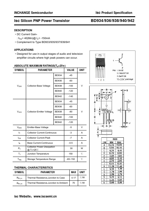
V A A A W ℃ ℃
PC TJ Tstg
THERMAL CHARACTERISTICS
SYMBOL Rth j-c Rth j-a PARAMETER Thermal Resistance,Junction to Case Thermal Resistance,Junction to Ambient MAX 4.17 70 UNIT ℃/W ℃/W
MHz
Switching Times ton toff Turn-On Time IC= -1.0A; IB1= -IB2= -0.1A Turn-Off Time 0.7 2.4 μs 0.2 0.6 μs
isc Website:
2
B
BD934/936/938/940/942
VALUE -45 -60 -100 -120 -140 -45 -60 -80 -100 -120 -5 -3 -7 -0.5 30 150 -65~150
UNIT
V
V
Emitter-Base Voltage Collector Current-Continuous Collector Current-Peak Base Current-Continuous Collector Power Dissipation @ TC=25℃ Junction Temperature Storage Temperature Range
TC=25℃ unless otherwise specified SYMBOL PARAMETER BD934 BD936 VCEO(SUS) Collector-Emitter Sustaining Voltage BD938 BD940 BD942 VCE(sat) VBE(on) ICBO ICEO IEBO hFE-1 hFE-2 fT Collector-Emitter Saturation Voltage Base-Emitter On Voltage Collector Cutoff Current Collector Cutoff Current Emitter Cutoff Current DC Current Gain DC Current Gain Current-Gain—Bandwidth Product IC= -1A; IB= -0.1nductor
电动托盘电机型号与功能介绍说明书

A I R C H ALODESTAR XL 2 to 7 1/2 tonn n n n n n n XL AIR 2 to 7 1/2 ton n n n n n nE V E R S P E C I A LOW HEADROOM CHAIN 1 to 24 tonn n Upper Shipyard Hook Lower Shipyard HookSERIES 6331/2 to 5 ton n Frames connected by steel equalizer pin, secured by two nuts on each side n Rugged steel side plates formed to include bumpersCBT1/4 to 5 ton n nn Bridge Crane Kits n Jib Cranesn LodeRail™Systems n Chain Containersn Cord Reelsn Festooning Packagesn Bronze Wheels / Hooks n Zinc Plated Chain / Hooks n Variable Speed Control n Stainless Steel Chain n NEMA Push Button Stations n Infrared Remote Control n Cady Spreader Beams n Plate Clamps nBinders n Herc Alloy Chain Slings n Hooks n Shackles n Hammerloks n Hoist Rings ACCESSORIES & PRODUCTS © 2012 Columbus McKinnon Corporation. All Rights Reserved. Stock # CMPG-0212 SS 5M GK Phone: (800) 888.0985•(716) 689.5400•Fax: (716) 689.5644•In addition to the strong knowledge base exemplified by comprehensive training programs, Columbus McKinnon is one of the only manufacturers supplying complete lifting systems to satisfy unique material handling requirements of users in a variety of environments. From jib cranes and hoists to chain slings, clamps, and related attachments;systems include products that are matched specifically to the lifting needs of the application. Products may also be modified in order to ensure that the proper system is in place for the job.Whether your needs call for a single electric chain hoist or a completely engineered system to outfit your production facility, Columbus McKinnon provides the products and expertise to keep your workforce productive and safe.。
938数显无铅焊台

938DESD数显无铅焊台
产品图片:
产品描述:
SLD-938DESD数显无铅焊台应用SLD焊接技术,采用高科技环保材料制造,在能耗、控温、回温及焊接质量都有优秀的表现,将传统焊台的效率提到一个新高度,确保在无铅焊接制程中得到更高效而可靠的焊接质量,是保证产品质量,提高生产效率,降低生产成本的首选产品。
产品特点:
采用三位一体数码管显示; 快速升温、回温迅速,特别适用于无铅焊接与低温焊接;人体工程学设计。
手柄轻巧,消除操作人员疲劳,安全可靠。
拆消静电设计。
焊咀拆卸方便,安装快捷。
分体式设计,摆放容易。
产品规格:
•功率:75W
•输入电压:AC220V (110V可选)
•输出电压:AC29V
•温度范围:200~480℃
•控制台:938DESD无铅焊台
•外形体积:120*93*170mm
•重量:1400g
产品应用:
半导体元件焊接、机板(PCB)制程、电子产品之组装制程焊接、电子制程之排线焊接、电子产品维修等普通焊接。
电子制程之半导体元件焊接
机板(PCB)制程
电子产品之组装制程焊接
电子制程之排线焊接
电子产品维修
深圳市新亚电子制程股份有限公司
地址:深圳市福田区荣超中心A栋9层
service@
400-700-9929。
单胞胎巴玛格卷绕机说明书

单胞胎巴玛格卷绕机说明书摘要:一、单胞胎巴玛格卷绕机简介二、单胞胎巴玛格卷绕机主要特点1.高效节能2.操作简便3.安全可靠4.高质量卷绕效果三、单胞胎巴玛格卷绕机适用范围四、单胞胎巴玛格卷绕机使用方法与注意事项1.安装与调试2.操作步骤3.维护与保养五、单胞胎巴玛格卷绕机故障排除六、售后服务与技术支持正文:一、单胞胎巴玛格卷绕机简介单胞胎巴玛格卷绕机是一款专为电线、电缆行业设计的自动化卷绕设备。
该设备具有高效、节能、操作简便、安全可靠等特点,可广泛应用于各种电线、电缆的卷绕加工。
二、单胞胎巴玛格卷绕机主要特点1.高效节能单胞胎巴玛格卷绕机采用先进的电机驱动技术,具有卓越的负载能力,确保在高效率的前提下,实现稳定卷绕。
2.操作简便该设备采用人性化设计,操作面板清晰易懂,使操作过程更加简便快捷。
同时,设备具有自动纠偏功能,有效提高卷绕精度。
3.安全可靠单胞胎巴玛格卷绕机采用高品质钢材制造,机身结构坚固,确保长时间运行稳定。
设备还配备了紧急停止按钮,以应对突发情况,确保人员安全。
4.高质量卷绕效果该设备采用双轴驱动,实现高精度的卷绕。
同时,卷绕张力可调,满足不同规格产品的卷绕需求,确保卷绕质量。
三、单胞胎巴玛格卷绕机适用范围单胞胎巴玛格卷绕机适用于各种电线、电缆的卷绕加工,如聚乙烯、聚氯乙烯、橡胶等材质的电线电缆。
广泛应用于电力、通信、交通、家电等行业。
四、单胞胎巴玛格卷绕机使用方法与注意事项1.安装与调试在使用前,请按照设备说明书进行安装和调试,确保各部件正常运转。
2.操作步骤1) 开启设备:打开电源开关,启动设备。
2) 设置参数:根据生产需求,设置卷绕速度、卷绕直径等参数。
3) 放入材料:将待卷绕的材料放入设备料架。
4) 开始卷绕:按下启动按钮,设备自动进行卷绕。
5) 卷绕结束:达到预定长度或厚度后,设备自动停止卷绕。
3.维护与保养1) 定期检查设备各部件,确保正常运转。
2) 定期给传动部位润滑,以延长使用寿命。
8AS170
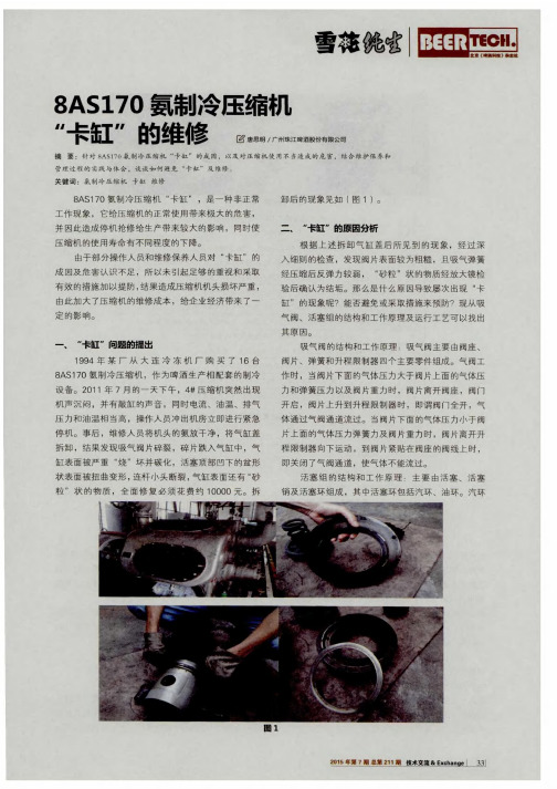
2)气 缸 垫 必 须 是 耐 压 石 棉 垫 ,最 好 是 使 用 生产 厂 家 提供 的 用 模 板 压 制 出来 的 。 因 为 自制 的 耐压 石 棉 垫 的厚 度 、 螺 丝 孔 的大 小 、工 艺孔 等难 于保 证 百 分 百 吻合 ,如 有 薄 弱 环 节 会 出现 受 高 压 气 体 影 响 而 泄 漏 。
油环与气缸 的间隙 ,经检测 ,其数据 分别见 ( 表 2) 。
2 、 装 配 过 程 将 活塞 取 出来 后 ,把 气 缸 内 的 “ 砂
粒 ” 、 吸 气 阀 片 碎 片清 理 干 净 , 同时 更 换 新 的 吸 气 阀
片及 其下面的弹簧 ,更换 气环、油环 、连杆 大小头的
轴 瓦 ,并 测 出 它 们 的间 隙。 具 体 数 据 见 如 ( 表 3) 。
四、 采 取 的措 施 和 工 艺调 整
隙, 因这个 数据 直接影响到单位容积制冷剂 的制 冷量 ,
根 据 公式 V =兀 / 4 D 2 S n Z( D 表 示 汽 缸 直 径 ,S
1 、建 立健全设 备的基础 管理制度 ,制订 出压缩
机 等 设 备 的维 护 保 养 、 润 滑 管 理 制 度 ,要 求 维 保 人 员 必须严格按照 8 A S 1 7 0氨 制冷 压 缩 机 的 使 用 说 明 书 的 要 求 进 行 大 、 中 、小 修 , 当压 缩 机 的 运 行 时 间 每 达 到
主轴 径 和 主轴 承 的 间 隙
O . O 9 0
0 . 1 2 l
曲轴与 主 轴 瓦 间窜动 量 表 4厂家装配间隙要求
部 位
上 部
1 . 2 5 0
1 7 0
型( 单位 :m m )
天泰紫光八开试卷胶订联动线技术参数

天泰紫光八开试卷胶订联动线技术参数
天泰紫光八开试卷胶订联动线是一种用于制作练习册、试卷等书籍的设备,具有以下技术参数:
1. 纸张尺寸范围:天泰紫光八开试卷胶订联动线适用于最大8开的纸张尺寸,即纵向高度不超过210mm,横向宽度不超过148mm。
2. 装订规格:该联动线可以实现胶订、精装订和无胶订三种装订方式。
胶订时,最大装订厚度通常不超过10mm。
3. 装订速度:天泰紫光八开试卷胶订联动线的装订速度通常在5000本/小时以上。
4. 电源要求:该设备通常使用380V/50Hz的三相交流电源。
5. 封背线材料:胶订时使用的封背线通常为热熔胶线。
6. 控制系统:天泰紫光八开试卷胶订联动线通常配备先进的数字化控制系统,可以实现自动化操作和调节,提高装订效率。
7. 尺寸及重量:具体尺寸和重量视具体型号而定。
请注意,以上参数仅为一般参考,具体的技术参数可能会因不同型号的设备而有所不同。
建议您参考具体的设备规格表或与设备厂家联系以获取准确的技术参数。
ANALOG DEVICES AD9387NK 数据手册

现货库存、技术资料、百科信息、热点资讯,精彩尽在鼎好!High Performance, Low PowerHDMI™/DVI Transmitter Preliminary Technical Data AD9387NKRev. PrAInformation furnished by Analog Devices is believed to be accurate and reliable. However, noresponsibility is assumed by Analog Devices for its use, nor for any infringements of patents or other rights of third parties that may result from its use. Specifications subject to change without notice. No license is granted by implication or otherwise under any patent or patent rights of Analog Devices. T rademarks and registered trademarks are the property of their respective owners. O ne Technology Way, P.O. Box 9106, Norwood, MA 02062-9106, U.S.A. Tel: 781.329.4700 Fax: 781.461.3113 ©2006 Analog Devices, Inc. All rights reserved.FEATURESGeneralLow power HDMI/DVI transmitter ideal for portable applicationsCompatible with HDMI v. 1.3, DVI v. 1.0, and HDCP v. 1.2 Single 1.8 V power supplyVideo/audio inputs accept logic levels from 1.8 V to 3.3 V 64-lead LFCSP, Pb-free package76-ball CSP_BGA, Pb-free packageDigital video80 MHz operation supports all resolutions from 480i to1080i and XGA at 75 HzProgrammable 2-way color space converterSupports RGB, YCbCr, and DDRSupports ITU656-based embedded syncsAutomatic input video format timing detection (CEA-861D) Digital audioSupports standard S/PDIF for stereo LPCM or compressed audio up to 192 kHz8-channel, uncompressed LPCM I2S audio up to 192 kHz Special features for easy system designOn-chip MPU with I2C® master to perform HDCPoperations and EDID reading operations5 V tolerant I2C and HPD I/Os, no extra device neededNo audio master clock needed for supporting S/PDIFand I2SOn-chip MPU reports HDMI events through interrupts and registersAPPLICATIONSDigital video camerasDigital still camerasPersonal media playersCellular handsetsDVD players and recordersDigital set-top boxesA/V receiversHDMI repeater/splitterGENERAL DESCRIPTIONThe AD9387NK is an 80 MHz, high definition multimedia interface (HDMI) v.1.3 transmitter. It supports HDTV formats up to 720p and 1080i and computer graphic resolutions up to XGA (1024 × 768 @ 75Hz). With the inclusion of HDCP, the AD9387NK allows the secure transmission of protected content, as specified by the HDCP v.1.1 protocol.FUNCTIONAL BLOCK DIAGRAMD[23:0]I2657-1Figure 1.The AD9387NK supports both S/PDIF and 8-channel I2S audio. Its high fidelity, 8-channel I2S can transmit either stereo or 7.1 surround audio at 192 kHz. The S/PDIF can carry stereo LPCM audio or compressed audio, including Dolby® Digital, DTS®, and THX®.The AD9387NK helps reduce system design complexity and cost by incorporating such features as an internal MPU for HDCP operations, an I2C master for EDID reading, a single 1.8 V power supply, and 5 V tolerance on the I2C and hot plug detect pins. Fabricated in an advanced CMOS process, the AD9387NK is available in a space saving, 76-ball CSP_BGA or 64-lead LFCSP surface-mount package. Both packages are available as Pb-free parts and are specified from −25°C to +85°C.AD9387NKPreliminary Technical DataRev. PrA | Page 2 of 12TABLE OF CONTENTSFeatures..............................................................................................1 Applications.......................................................................................1 General Description.........................................................................1 Functional Block Diagram..............................................................1 Specifications.....................................................................................3 Absolute Maximum Ratings............................................................4 Explanation of Test Levels...........................................................4 ESD Caution..................................................................................4 Pin Configuration and Function Descriptions.............................5 Applications Information................................................................7 Design Resources..........................................................................7 Document Conventions...............................................................7 PCB Layout Recommendations.......................................................8 Power Supply Bypassing...............................................................8 Digital Inputs.................................................................................8 External Swing Resistor................................................................8 Output Signals...............................................................................8 Outline Dimensions..........................................................................9 Ordering Guide.. (9)Preliminary Technical DataAD9387NKRev. PrA | Page 3 of 12SPECIFICATIONSTable 1.AD9387NK-BCPZ-80/AD9387NK-BBCZ-80Parameter Conditions Temp Test Level 1Min Typ Max Unit DIGITAL INPUTS Input Voltage, High (V IH ) Full VI 1.4 3.5 V Input Voltage, Low (V IL ) Full V I 0.7 V Input Capacitance 25°C V 3 pF DIGITAL OUTPUTS Output Voltage, High (V OH ) Full V I V DD − 0.1 V Output Voltage, Low (V OL ) Full V I 0.4 V THERMAL CHARACTERISTICS Thermal Resistance θJC Junction-to-Case V 15.2 °C/W θJA Junction-to-Ambient V 59 °C/W Ambient Temperature Full V −25 +25 +85 °C DC SPECIFICATIONS Input Leakage Current (I IL ) 25°C V I −10 +10 μA Input Clamp Voltage −16 mA 25°C V −0.8 V +16 mA 25°C V +0.8 V Differential High Level Output Voltage V AV CC V Differential Output Short-Circuit Current IV 10 μA POWER SUPPLY V DD (All) Supply Voltage Full IV 1.71 1.8 1.89 V V DD Supply Voltage Noise Full V 50 mV p-p Power-Down Current 25°C IV 10 μATransmitter Supply Current 225°C I V 55 mA Transmitter Total Power Full VI 100 mW AC SPECIFICATIONS CLK Frequency 25°C IV 13.5 80 MHz TMDS Output CLK Duty Cycle 25°C IV 48 52 % Worst Case CLK Input Jitter Full IV 2 ns Input Data Setup Time Full IV 1 ns Input Data Hold Time Full IV 1 ns TMDS Differential Swing VI 800 1000 1200 mV VSYNC and HSYNC Delay from DE Falling Edge VI 1 UI 3VSYNC and HSYNC Delay to DE Rising Edge VI 1 UI 3DE High Time 25°C VI 8191 UI 3DE Low Time 25°C VI 138 UI 3Differential Output Swing Low-to-High Transition Time 25°C VII 75 490 Ps High-to-Low Transition Time 25°C VII 75 490 Ps AUDIO AC TIMINGSample Rate I 2S and S/PDIF Full IV 32 192 kHz I 2S Cycle Time 25°C IV 1 UI 3I 2S Setup Time 25°C IV 15 ns I 2S Hold Time 25°C IV 0 ns Audio Pipeline Delay 25°C IV 75 μs1 See the Explanation of Test Levels section. 2Using low output drive strength. 3UI = unit interval.AD9387NKPreliminary Technical DataRev. PrA | Page 4 of 12ABSOLUTE MAXIMUM RATINGSTable 2.Parameter RatingDigital Inputs 5 V to 0.0 VDigital Output Current 20 mAOperating Temperature Range −40°C to +85°C Storage Temperature Range −65°C to +150°C Maximum Junction Temperature 150°CMaximum Case Temperature 150°CStresses above those listed under Absolute Maximum Ratingsmay cause permanent damage to the device. This is a stress rating only; functional operation of the device at these or any other conditions above those indicated in the operationalsection of this specification is not implied. Exposure to absolute maximum rating conditions for extended periods may affect device reliability.EXPLANATION OF TEST LEVELSI. 100% production tested. II. 100% production tested at 25°C and sample tested atspecified temperatures.III. Sample tested only. IV . Parameter is guaranteed by design and characterization testing.V . Parameter is a typical value only.VI. 100% production tested at 25°C; guaranteed by design and characterization testing.VII.Limits defined by HDMI specification; guaranteed by design and characterization testing.ESD CAUTIONPreliminary Technical DataAD9387NKRev. PrA | Page 5 of 12PIN CONFIGURATION AND FUNCTION DESCRIPTIONS17181920212223242526272829303132P V D D E X T _S W G A V D D H P D T x C –T x C +A V D D T x 0–T x 0+P D /A 0T x 1–T x 1+A V D D T x 2–T x 2+I N T 64636261605958575655545352515049D G N D D 1D 2D 3D 4D 5D 6D 7D 8D 9D 10D 11D 12D 13D 14D V D D12345678910111213141516DVDDD0DE HSYNC VSYNC CLK S/PDIF MCLK I 2S0I 2S1I 2S2I 2S3SCLK LRCLK PVDD PVDD DVDD D15D16D17D18D19D20D21D22D23MCL MDA SDA SCLDDCSDA DDCSCL4847464544434241403938373635343306507-002NOTES1. GND PADDLE ON BOTTOM OF PACKAGE.Figure 2. 64-Lead LFCSP Pin Configuration (Top View)A B C D E F G J H K10876321954BOTTOM VIEW (Not to Scale)06507-003Figure 3. 76-Ball BGA Configuration (Top View)Table 3. Pin Function DescriptionsPin No.BGA LFCSPMnemonic Type 1Description A1 to A10, B1 to B10, C9, C10, D9, D10 39 to 47,50 to 63, 2 D[23:0] I Video Data Input. Digital input in RGB or YCbCr format. Supports CMOS logic levels from 1.8 V to 3.3 V. D1 6 CLK I Video Clock Input. Supports CMOS logic levels from 1.8 V to 3.3 V. C2 3 DE I Data Enable Bit for Digital Video. Supports CMOS logic levels from 1.8 V to 3.3 V. C1 4 HSYNC I Horizontal Sync Input. Supports CMOS logic levels from 1.8 V to 3.3 V. D2 5 VSYNC I Vertical Sync Input. Supports CMOS logic levels from 1.8 V to 3.3 V. J3 18 EXT_SWG I Sets internal reference currents. Place 887 Ω resistor (1% tolerance) between thispin and ground.K3 20 HPD I Hot Plug Detect Signal. This indicates to the interface if the receiver isconnected. Supports CMOS logic levels from 1.8 V to 5.0 V.E2 7 S/PD I F I S/PDIF (Sony/Philips Digital Interface) Audio Input. This is the audio input from aSony/Philips digital interface. Supports CMOS logic levels from 1.8 V to 3.3 V.E1 8 MCLK I Audio Reference Clock. 128 × N × f S with N = 1, 2, 3, or 4. Set to 128 × samplingfrequency (f S ), 256 × f S , 384 × f S , or 512 × f S . Supports CMOS logic levels from 1.8 V to 3.3 V.F2, F1, G2, G1 9 to 12 I 2S[3:0] I I 2S Audio Data Inputs. These represent the eight channels of audio (two perinput) available through I 2S. Supports CMOS logic levels from 1.8 V to 3.3 V. H2 13 SCLK I I 2S Audio Clock. Supports CMOS logic levels from 1.8 V to 3.3 V. H1 14 LRCLK I Left/Right Channel Selection. Supports CMOS logic levels from 1.8 V to 3.3 V. J7 26 PD/A0 I Power-Down Control and I 2C Address Selection. The I 2C address and the PDpolarity are set by the PD/A0 pin state when the supplies are applied to the AD9387NK. Supports CMOS logic levels from 1.8 V to 3.3 V.K1, K2 21, 22 TxC−/TxC+ O Differential Clock Output. Differential clock output at pixel clock rate; TMDSlogic level.K10, J10 30, 31 Tx2−/Tx2+ O Differential Output Channel 2. Differential output of the red data at 10× the pixelclock rate; TMDS logic level.AD9387NKPreliminary Technical DataRev. PrA | Page 6 of 12Pin No.BGA LFCSPMnemonic Type 1DescriptionK7, K8 27, 28 Tx1−/Tx1+ ODifferential Output Channel 1. Differential output of the green data at 10× the pixel clock rate; TMDS logic level.K4, K5 24, 25 Tx0−/Tx0+ O Differential Output Channel 0. Differential output of the blue data at 10× thepixel clock rate; TMDS logic level.H10 32 I NT O Interrupt. Open drain. A 2 kΩ pull-up resistor to the microcontroller I/O supply isrecommended.J2, J5, J8, K9 19, 23, 29 AVDD P 1.8 V Power Supply for TMDS Outputs. D5, D6, D7, E7 1,48,49 DVDD P 1.8 V Power Supply for Digital and I/O Power Supply. These pins supply power tothe digital logic and I/Os. They should be filtered and as quiet as possible.G4, G5, J1 15, 16, 17 PVDD P 1.8 V PLL Power Supply. The most sensitive portion of the AD9387NK is the clockgeneration circuitry. These pins provide power to the clock PLL. The designer should provide quiet, noise-free power to these pins.D4, E4, F4, J4, G6, J6, K6, F7, G7, H9, J9 64, Paddle on bottom side GND P Ground. The ground return for all circuitry on-chip. It is recommended that the AD9387NK be assembled on a single, solid ground plane with careful attention given to ground current paths.F9 36 SDA C 2Serial Port Data I/O. This pin serves as the serial port data I/O slave for registeraccess. Supports CMOS logic levels from 1.8V to 3.3V.F10 35 SCL C 2Serial Port Data Clock. This pin serves as the serial port data clock slave forregister access. Supports CMOS logic levels from 1.8V to 3.3V.E10 37 MDA C 2Serial Port Data I/O Master to HDCP Key EEPROM. Supports CMOS logic levelsfrom 1.8 V to 3.3 V.E9 38 MCL C 2Serial Port Data Clock Master to HDCP Key EEPROM. Supports CMOS logic levelsfrom 1.8 V to 3.3 V.G9 34 DDCSDA C 2Serial Port Data I/O to Receiver. This pin serves as the master to the DDC bus.Supports 5 V CMOS logic level.G10 33 DDCSCL C 2Serial Port Data Clock to Receiver. This pin serves as the master clock for the DDCbus. Supports 5 V CMOS logic level.1 I = input, O = output, P = power supply, C = control.2For a full description of the 2-wire serial interface and its functionality, obtain documentation by contacting NDA from *************************.Preliminary Technical DataAD9387NKRev. PrA | Page 7 of 12APPLICATIONS INFORMATIONDESIGN RESOURCESAnalog Devices, Inc. evaluation kits, reference design schematics, and other support documentation are available under NDA from *************************. Other resources include the following: •EIA/CEA-861D , a technical specifications document that describes audio and video infoframes, as well as the E-EDID structure for HDMI. It is available from the Consumer Electronics Association (CEA).•HDMI v. 1.3, a defining document for HDMI 1.3, and HDMI Compliance Test Specification v. 1.3. They are available from HDMI Licensing, LLC.•HDCP Specification v1.1, the defining technical specifications document for the HDCP v. 1.1. It is available from Digital Content Protection, LLC.DOCUMENT CONVENTIONSIn this data sheet, data is represented using the conventions described in Table 4.Table 4. Document ConventionsDataType Format0xNN Hexadecimal (Base 16) numbers are represented usingthe C language notation, preceded by 0x.0bNN Binary (Base 2) numbers are represented using the Clanguage notation, preceded by 0b.NN Decimal (Base 10) numbers are represented using noadditional prefixes or suffixes.Bit Bits are numbered in little endian format; that is, theleast significant bit of a byte or word is referred to as Bit 0.AD9387NKRev. PrA | Page 8 of 12PCB LAYOUT RECOMMENDATIONSThe AD9387NK is a high precision, high speed analog device. For maximum performance, it is important that board layout be optimized.POWER SUPPLY BYPASSINGIt is recommended that each power supply pin be bypassed with a 0.1 μF capacitor. The exception is when two or more supply pins are adjacent to each other. For these groupings of powers and grounds, it is necessary to have only one bypass capacitor. The fundamental idea is to have a bypass capacitor within about 0.5 cm of each power pin. Avoid placing the capacitor on the opposite side of the PC board from the AD9387NK, as doing so interposes resistive vias in the path. The bypass capacitors should be located between the power plane and the power pin. Current should flow from the power plane to the capacitor to the power pin. Do not make a power connection between the capacitor and the power pin. Placing a via underneath the capacitor pads, down to the power plane, is generally the best approach.It is particularly important to maintain low noise and good stability of PVDD (the PLL supply). Abrupt changes in PVDD can result in similarly abrupt changes in sampling clock phase and frequency. Such changes can be avoided by careful attention to regulation, filtering, and bypassing. It is best practice to provide separate regulated supplies for each of the analog circuitry groups (AVDD and PVDD).It is also recommended that a single ground plane be used for the entire board. Experience has repeatedly shown that the noise performance is the same or better with a single ground plane. Using multiple ground planes can be detri-mental because each separate ground plane is smaller, and long ground loops can result.DIGITAL INPUTSVideo and Audio Data Input SignalsThe digital inputs on the AD9387NK are designed to work with signals ranging from 1.8 V to 3.3 V logic level. Therefore, no extra components need to be added when using 3.3 V logic. Any noise that gets onto the clock input (labeled CLK) trace adds jitter to the system. Therefore, minimize the video clock input (Pin 6, CLK) trace length, and do not run any digital or other high frequency traces near it. Make sure to match the length of the input data signals to optimize data capture, especially for high frequency modes, such as 720p or XGA at 75 Hz and double data rate input formats.Other Input SignalsThe HPD must be connected to the HDMI connector. A 10 kΩ pull-down resistor to ground is also recommended.The PD/A0 input pin can be connected to GND or supply (through a resistor or a control signal). The device address and power-down polarity are set by the state of the PD/A0 pin when the AD9387NK supplies are applied/enabled. For example, if the PD/A0 pin is low (when the supplies are turned on), then the device address is 0x72 and the power-down is active high. If the PD/A0 pin is high (when the supplies are turned on), the device address is 0x7A and the power down is active low. The SCL and SDA pins should be connected to the I 2C master. A pull-up resistor of 2 kΩ to 1.8 V or 3.3 V is recommended.EXTERNAL SWING RESISTORThe external swing resistor must be connected directly to the EXT_SWG pin and ground. The external swing resistor must have a value of 887 Ω (±1% tolerance). Avoid running any high speed ac or noisy signals next to, or close to, the EXT_SWG pin.OUTPUT SIGNALSTMDS Output SignalsThe AD9387NK has three TMDS data channels (0, 1, and 2) that output signals up to 800 MHz, as well as the TMDS output data clock. To minimize the channel-to-channel skew, make the trace length of these signals the same. Also, these traces need a 50 Ω characteristic impedance and should be routed as 100 Ω differential pairs. Best practice recommends routing these lines on the top PCB layer, avoiding the use of vias.Other Output Signals (non TMDS) DDCSCL and DDCSDAThe DDCSCL and DDCSDA outputs need a minimum amount of capacitance loading to ensure the best signal integrity. The DDCSCL and DDCSDA capacitance loading must be less than 50 pF to meet the HDMI compliance specification. The DDCSCL and DDCSDA must be connected to the HDMI connector, and a pull-up resistor to 5 V is required. The pull-up resistor must have a value between 1.5 kΩ and 2 kΩ.INT PinThe INT pin is an output that should be connected to the system microcontroller. A pull-up resistor to 1.8 V or 3.3 V is required for proper operation; the recommended value is 2 kΩ.MCL and MDAThe MCL and MDA outputs should be connected to the EEPROM containing the HDCP key (if HDCP is implemented). Pull-up resistors of 2 kΩ are recommended.Preliminary Technical DataAD9387NKRev. PrA | Page 9 of 12OUTLINE DIMENSIONS*COMPLIANT TO JEDEC STANDARDS MO-220-VMMD EXCEPT FOR EXPOSED PAD DIMENSIONPLANEDIMENSIONS in Millimeters64 LFCSP (LEAD FRAME CHIP SCALE PACKAGE)**Note: PAD is CONNECTED to GNDFigure 4. 64-Lead Lead Frame Chip Scale Package [LFCSP](CP-64)Dimensions shown in millimeters*COMPLIANT TO JEDEC STANDARDS MO-225 WITH THE EXCEPTION TO PACKAGE HEIGHT.BALL DIAMETER*012006-0Figure 5. 76-Ball Chip Scale Package Ball Grid Array [CSP_BGA]6 mm × 6 mm × 1.4 mm(BC-76)Dimensions shown in millimetersORDERING GUIDEModelTemperature Range Package DescriptionPackage Option AD9387NKBCPZ-801−25°C to +85°C 64-Lead Formed Chip Scale PackageCP-64AD9387NKBBCZ-801−25°C to +85°C76-Ball Chip Scale Package Ball Grid Array [CSP_BGA] BC-76 AD9387NKBBCZRL-801−25°C to +85°C 76-Ball Chip Scale Package Ball Grid Array [CSP_BGA] BC-76AD9387NK/PCBEvaluation Board1Z = Pb-free part.AD9387NKNOTESRev. PrA | Page 10 of 12Preliminary Technical Data AD9387NK NOTESRev. PrA | Page 11 of 12AD9387NKRev. PrA | Page 12 of 12 NOTESPurchase of licensed I 2C components of Analog Devices or one of its sublicensed Associated Companies conveys a license for the purchaser under the Philips I 2C Patent Rights to use these components in an I 2C system, provided that the system conforms to the I 2C Standard Specification as defined by Philips.©2006 Analog Devices, Inc. All rights reserved. Trademarks andregistered trademarks are the property of their respective owners.PR06507-0-12/06(PrA)。
- 1、下载文档前请自行甄别文档内容的完整性,平台不提供额外的编辑、内容补充、找答案等附加服务。
- 2、"仅部分预览"的文档,不可在线预览部分如存在完整性等问题,可反馈申请退款(可完整预览的文档不适用该条件!)。
- 3、如文档侵犯您的权益,请联系客服反馈,我们会尽快为您处理(人工客服工作时间:9:00-18:30)。
10-Bit Integrated, Multiformat, HDTV Video Decoder,RGB Graphics Digitizer, and 2:1 MultiplexedHDMI/DVI InterfaceAD9388AInformation furnished by Analog Devices is believed to be accurate and reliable. However, noresponsibility is assumed by Analog Devices for its use, nor for any infringements of patents or other rights of third parties that may result from its use. Specifications subject to change without notice. No license is granted by implication or otherwise under any patent or patent rights of Analog Devices. T rademarks and registered trademarks are the property of their respective owners. One Technology Way, P.O. Box 9106, Norwood, M A 02062-9106, U.S.A. Tel: 781.329.4700 Fax: 781.461.3113 ©2007–2008 Analog Devices, Inc. All rights reserved.FEATURESMutliformat decoderThree 10-bit analog-to-digital converters (ADCs)ADC sampling rates up to 170 MHzMux with 12 analog input channels525i-/625i-component SD support525p-/625p-component progressive scan support720p-/1080i-/1080p-component HDTV support Digitizes RGB graphics up to 1600 × 1200 at 60 Hz (UXGA) VBI data slicer (including teletext)Analog-to-HDMI fast switchingDual High-Definition Multimedia Interface (HDMI) Rx2:1 multiplexed HDMI receiverHDMI 1.3, DVI 1.0225 MHz HDMI receiverRepeater supportHigh-bandwidth digital content protection (HDCP 1.3) 36-bit deep color supportS/PDIF (IEC60958-compatible) digital audio output Multichannel I2S audio output (up to 8 channels) Adaptive equalizer for cable lengths up to 30 meters Internal EDID RAMGeneralHighly flexible output interfaceSTDI function support standard identification2 any-to-any3 × 3 color-space conversion matrices Programmable interrupt request output pins APPLICATIONSAdvanced TVsPDP HDTVsLCD TVs (HDTV ready)LCD/DLP® rear projection HDTVsCRT HDTVsLCoS® HDTVsAudio/video receivers (AVRs)LCD/DLP front projectorsHDTV STBs with PVRDVD recorders with progressive scan input support GENERAL DESCRIPTIONThe AD9388A is a high quality, single-chip graphics digitizer with an integrated 2:1 multiplexed HDMI™ receiver.The AD9388A contains one main component processor (CP) that processes YPrPb and RGB component formats, including RGB graphics. The CP also processes the video signals from the HDMI receiver. The AD9388A can keep the HDCP link between an HDMI source and the selected HDMI port active in analog mode operation. This allows for fast switching between the analog and HDMI modes.The AD9388A supports the decoding of a component RGB or YPrPb video signal into a digital YCrCb or RGB pixel output stream. The support for component video includes 525i, 625i, 525p, 625p, 720p, 1080i, 1080p, and 1250i standards, as well as many other HD and SMPTE standards.Graphic digitization is also supported by the AD9388A. TheAD9388A is capable of digitizing RGB graphics signals from VGA to UXGA rates and converting them into a digital RGBor YCrCb pixel output stream.The AD9388A incorporates a dual input, HDMI 1.3-compatible receiver that supports HDTV formats up to 1080p and display resolutions up to UXGA (1600 × 1200 at 60 Hz). The reception of encrypted video is possible with the inclusion of HDCP. In addition, the inclusion of adaptive equalization ensures robust operation of the interface with cable lengths up to 30 meters. The HDMI receiver has an advanced audio functionality, such as a mute controller that prevents audible extraneous noise in the audio output.Derivative parts of the AD9388A are available; AD9388ABSTZ-A5 is composed of one analog and one digital input. To facili-tate professional applications, where HDCP processing and decryption are not required, the AD9388ABSTZ-5P derivative is available. This allows users who are not HDCP adopters to purchase the AD9388A. See the Ordering Guide for details on these derivative parts.Fabricated in an advanced CMOS process, the AD9388A is available in a space saving, 144-lead, surface-mount, RoHS-compliant, plastic LQFP and is specified over the −40°C to+85°C temperature range.AD9388ARev. B | Page 2 of 28TABLE OF CONTENTSFeatures .............................................................................................. 1 Applications ....................................................................................... 1 General Description ......................................................................... 1 Revision History ............................................................................... 2 Functional Block Diagram .............................................................. 3 Specifications ..................................................................................... 4 Electrical Characteristics ............................................................. 4 Analog and HDMI Specifications .............................................. 6 Data and I 2C Timing Characteristics ......................................... 7 Absolute Maximum Ratings ............................................................ 9 Thermal Resistance ...................................................................... 9 Package Thermal Performance ................................................... 9 ESD Caution .................................................................................. 9 Pin Configurations and Function Descriptions ......................... 10 Functional Overview ...................................................................... 16 Analog Front End ....................................................................... 16 HDMI Receiver (16)Component Processor Pixel Data Output Modes .................. 16 Component Video Processing .................................................. 16 RGB Graphics Processing ......................................................... 16 General Features ......................................................................... 16 Theory of Operation ...................................................................... 17 Analog Front End ....................................................................... 17 HDMI Receiver ........................................................................... 17 Component Processor (CP) ...................................................... 17 VBI Data Processor .................................................................... 17 Pixel Output Formatting................................................................ 18 Register Map Architecture ........................................................ 21 Typical Connection Diagram ................................................... 22 Recommended External Loop Filter Components ................ 23 AD9388A/ADV7441A Evaluation Platform .............................. 24 Outline Dimensions ....................................................................... 25 Ordering Guide .. (25)REVISION HISTORY7/08—Rev. SpA to Rev. B5/08—Rev. Sp0 to Rev. SpAChanges to General Description .................................................... 1 Added Figure 6 ................................................................................ 13 Added Table 7 .................................................................................. 13 Changes to Component Processor Pixel Data Output Modes Section .............................................................................................. 16 Changes to Component Processor (CP) Section........................ 17 Added AD9388A/ADV7441A Evaluation Platform Section .... 24 Changes to Ordering Guide .......................................................... 25 10/07—Revsion Sp0: Initial VersionAD9388ARev. B | Page 3 of 28FUNCTIONAL BLOCK DIAGRAM06915-001R X A _R X A _R X A _R X B _R X B _R X A _R X B _R X B _D D C A _S D D C A _S D D D C B _S D D D C B _S 0 T O 910 T O 1920 T O 29N T 1S /C SS /F I E L DE /F I E L DCN C _O U T /T 2L AFigure 1.元器件交易网AD9388ASPECIFICATIONSELECTRICAL CHARACTERISTICSAVDD = 1.71 V to 1.89 V, DVDD = 1.62 V to 1.98 V, DVDDIO = 2.97 V to 3.63 V, PVDD = 1.71 V to 1.89 V, TVDD = 3.135 V to 3.465 V, CVDD = 1.71 V to 1.89 V. Operating temperature range is −40°C to +85°C, unless otherwise noted.Rev. B | Page 4 of 28AD9388ARev. B | Page 5 of 28Parameter 1Symbol Test Conditions M in Typ Max Unit TMDS PLL and Equalizer Supply Current YPrPb 1080p sampling @ 148.5 MHz 6 56 79 mAHDMI RGB sampling @ 165 MHz 7, 8 86 105 mAHDMI RGB sampling @ 225 MHz 7, 8 95 118 mA Analog Supply Current I AVDD Graphics RGB sampling @ 108 MHz 6 174 278 mA YPrPb 1080p sampling @ 148.5 MHz 6 180 284 mA HDMI RGB sampling @ 165 MHz 7, 8 0 2 mAHDMI RGB sampling @ 225 MHz 7, 8 0 2 mA Terminator Supply Current I TVDD Graphics RGB sampling @ 108 MHz 6 12 18 mA YPrPb 1080p sampling @ 148.5 MHz 6 12 18 mA HDMI RGB sampling @ 165 MHz 7, 8, 9 42 47 mAHDMI RGB sampling @ 225 MHz 7, 8, 9 63 69 mA Audio and Video Supply Current I PVDD Graphics RGB sampling @ 108 MHz 6 14 21 mA YPrPb 1080p sampling @ 148.5 MHz 6 19 24 mA HDMI RGB sampling @ 165 MHz 7, 8 10 19 mAHDMI RGB sampling @ 225 MHz 7, 8 15 20 mA Power-Down Current I PWRDN 11.6 mA Power-Up Timet PWRUP25 ms1 The minimum/maximum specifications are guaranteed over the −40°C to +85°C temperature range (T MIN to T MAX ).2All ADC linearity tests performed at input range of full scale − 12.5% and at zero scale + 12.5%. 3Pin 1, Pin 105, Pin 106, and Pin 144 are 5 V tolerant. 4Guaranteed by characterization. 5V OH and V OL levels obtained using default drive strength value (0x15) in User Map Register 0xF4. 6Current measurements for analog inputs were made with HDMI/analog simultaneous mode disabled (User Map Register 0xBA Bit 7 programmed with Value 0) and no HDMI sources connected to the part. 7Current measurements for HDMI inputs were made with a source connected to the active HDMI port and no source connected to the inactive HDMI port. 8Audio stream is uncompressed stereo audio sampling frequency of f S = 48 kHz and MCLKOUT = 256 f S . 9The terminator supply current may vary with the HDMI source in use.AD9388ARev. B | Page 6 of 28ANALOG AND HDMI SPECIFICATIONSAVDD = 1.71 V to 1.89 V , DVDD = 1.62 V to 1.98 V , DVDDIO = 2.97 V to 3.63 V , PVDD = 1.71 V to 1.89 V , TVDD = 3.135 V to 3.465 V , CVDD = 1.71 V to 1.89 V . Operating temperature range is −40°C to +85°C, unless otherwise noted. Table 2.Parameter 1, 2Test Conditions Min Typ Max Unit ANALOG Clamp Circuitry External Clamp Capacitor 0.1 μF Input Impedance (Except Pin 74) Clamps switched off 10 MΩ Input Impedance of Pin 74 20 kΩ CML 0.88 V ADC Full-Scale Level CML + 0.5 V ADC Zero-Scale Level CML − 0.5 V ADC Dynamic Range 1 V Clamp Level (When Locked) Component input (Y signal) CML − 0.120 V Component input (Pr signal) CML V Component input (Pb signal) CML V PC RGB input (R, G, B signals) CML − 0.120 VHDMI SPECIFICATIONS 3Intrapair (Positive-to-Negative) Differential Input Skew 0.4 t bit 4Channel-to-Channel Differential Input Skew 0.2 t pixel 5 + 1.78 ns1 The minimum/maximum specifications are guaranteed over the −40°C to +85°C temperature range. 2Guaranteed by characterization. 3Guaranteed by design. 4t bit is 1/10 the pixel period of the TMDS clock. 5t pixel is the period of the TMDS clock.AD9388ARev. B | Page 7 of 28DATA AND I 2C TIMING CHARACTERISTICSAVDD = 1.71 V to 1.89 V , DVDD = 1.62 V to 1.98 V , DVDDIO = 2.97 V to 3.63 V , PVDD = 1.71 V to 1.89 V , TVDD = 3.135 V to 3.465 V , CVDD = 1.71 V to 1.89 V; operating temperature range is −40°C to +85°C, unless otherwise noted. Table 3.Parameter 1, 2Symbol Test Conditions M inTyp Max UnitSYSTEM CLOCK AND CRYSTAL Crystal Nominal Frequency 28.6363 MHz Crystal Frequency Stability±50 ppm Horizontal Sync Input Frequency 14.8 110 kHz LLC Frequency Range 12.825 170 MHz I 2C PORTS (FAST MODE)3xCL Frequency 4400 kHz xCL Minimum Pulse Width High 4t 1 0.6 μs xCL Minimum Pulse Width Low 4t 2 1.3 μs Hold Time (Start Condition) t 3 0.6 μs Setup Time (Start Condition) t 4 0.6 μs xDA Setup Time 4t 5 100 ns xCL and xDA Rise Times 4t 6 300 ns xCL and xDA Fall Times 4t 7 300 ns Setup Time (Stop Condition) t 8 0.6 μs I 2C PORTS (NORMAL MODE)xCL Frequency100 kHz xCL Minimum Pulse Width High t 1 4 μs xCL Minimum Pulse Width Low t 2 4.7 μs Hold Time (Start Condition) t 3 4 μs Setup Time (Start Condition) t 4 4.7 μs xDA Setup Timet 5 250 ns xCL and xDA Rise Times t 6 1000 ns xCL and xDA Fall Timest 7 300 ns Setup Time (Stop Condition) t 8 4 μs RESET FEATURE Reset Pulse Width 5 ms CLOCK OUTPUTSLLC Mark Space Ratiot 9:t 1045:55 55:45 % duty cycleDATA AND CONTROL OUTPUTSData Output Transition Time SDR (CP)5t 11 End of valid data to negative clock edge 2 ns t 12 Negative clock edge to start of valid data 0.5 ns I 2S PORT (MASTER MODE)SCLK Mark Space Ratio t 13:t 1445:55 55:45 % duty cycleLRCLK Data Transition Time t 15End of valid data to negative SCLK edge 10 ns LRCLK Data Transition Time t 16Negative SCLK edge to start of valid data 10 ns I2Sx Data Transition Time 6t 17End of valid data to negative SCLK edge 5 ns I2Sx Data Transition Time 6t 18Negative SCLK edge to start of valid data 5 ns MCLKOUT Frequency4.096 24.576 MHz1 The minimum/maximum specifications are guaranteed over the −40°C to +85°C temperature range (T MIN to T MAX ).2Guaranteed by characterization. 3Refers to all I 2C pins (DDC and control port). 4The prefix x refers to pin names beginning with S, DDCA_S, and DDCB_S. 5CP timing figures were obtained using the maximum drive strength value (0x3F) in User Map Register 0xF4. 6The suffix x refers to pin names ending with 0, 1, 2, and 3.AD9388ARev. B | Page 8 of 28Timing Diagrams6915-002NOTES1. THE PREFIX x REFERS TO PIN NAMES BEGINNING WITH S, DDCA_S, AND DDCB_S.Figure 2. I 2C TimingLLCP0TO P29, VS,HS, FIELD/DE06915-004Figure 3. Pixel Port and Control CP Output Timing (CP Core)I 2NOTES06915-005Figure 4. I 2S TimingAD9388ARev. B | Page 9 of 28ABSOLUTE MAXIMUM RATINGSTHERMAL RESISTANCETable 4.Parameter Rating AVDD to AGND 2.2 V DVDD to DGND 2.2 V PVDD to PGND 2.2 V DVDDIO to DGND 4 V CVDD to CGND 2.2 V TVDD to TGND 4 V DVDDIO to AVDD −0.3 V to +3.6 V DVDDIO to TVDD −3.6 V to +3.6 V DVDDIO to DVDD −2 V to +2 V CVDD to DVDD −2 V to +0.3 V PVDD to DVDD −2 V to +0.3 V AVDD to CVDD −2 V to +2 V AVDD to PVDD −2 V to +2 V AVDD to DVDD −2 V to +2 V AVDD to TVDD −3.6 V to +0.3 V TVDD to DVDD −2 V to +2 V Digital InputsVoltage to DGND DGND − 0.3 V to DVDDIO + 0.3 V Digital OutputsVoltage to DGNDDGND − 0.3 V to DVDDIO + 0.3 V Analog InputsVoltage to AGNDAGND − 0.3 V to AVDD + 0.3 V Maximum JunctionTemperature (T J _MAX ) 125°C Storage Temperature Range −65°C to +150°C Infrared Reflow,Soldering (20 sec)260°C Table 5.Package TypeΨJT 1 Unit144-Lead LQFP (ST-144)1.62 °C/W1Junction-to-package surface thermal resistance.PACKAGE THERMAL PERFORMANCETo reduce power consumption during AD9388A operation,turn off unused ADCs.On a four-layer PCB that includes a solid ground plane, the θJA value is 25.3°C/W . However, due to variations within the PCB metal and, therefore, variations in PCB heat conductivity, the value of θJA may differ for various PCBs.The most efficient measurement technique is to use the surface temperature of the package to estimate the die temperature because this is not affected by the variance associated with the θJA value.The maximum junction temperature (T J _MAX ) of 125°C must not be exceeded. The following equation calculates the junction temperature using the measured surface temperature of the package and applies only when no heat sink is used on DUT:T J _MAX = T S + (ΨJT × W TOTAL )where:T S is the surface temperature of the package expressed in degrees Celsius.ΨJT is the junction-to-package surface thermal resistance.W TOTAL = {(A VDD × IA VDD ) + (DVDD × IDVDD ) + (DVDDIO × IDVDDIO ) + (PVDD × IPVDD ) + (CVDD × ICVDD ) + (TVDD × ITVDD )}.Stresses above those listed under Absolute Maximum Ratings may cause permanent damage to the device. This is a stress rating only; functional operation of the device at these or any other conditions above those indicated in the operationalsection of this specification is not implied. Exposure to absolute maximum rating conditions for extended periods may affect device reliability. Contact an Analog Devices, Inc., representative for more details on package thermal performance at video.products@ .ESD CAUTIONAD9388ARev. B | Page 10 of 28PIN CONFIGURATIONS AND FUNCTION DESCRIPTIONSDDCB_SDASPDIF I2S0I2S1I2S2I2S3LRCLK SCLK MCLKOUT EXT_CLAMPSDA SCL ALSB DGND DVDDIO DE/FIELDHS/CS VS/FIELDINT1SYNC_OUT/INT2RESET DGND DVDDP0P1P2P3P4P5P6P7P8P9DGND DVDDIOP10TEST0TEST1SOG AIN7AIN1AIN8AIN2AIN9AIN3AGND AGND AVDD REFOUT CML AGND AVDD TEST2REFN TEST3REFP AIN10AIN4AIN11AIN5SOY AIN12AIN6PGND PVDD AUDIO_ELPF CGNDCVDD DDCA_SCL DDCA_SDA TEST4TEST5C V D DC G ND T V D D R X A _C N R X A _C P T G N D R X A _0N R X A _0P T G N D R X A _1N R X A _1P T G N D R X A _2N R X A _2P T V D D R TE R M C V D D C G N D T V D D R X B _C N R X B _C P T G N D R X B _0N R X B _0P T G N D R X B _1N R X B _1P T G N D R X B _2N R X B _2P T V D D C G N D C V D D D V D D D G N D D D C B _S C L P 11P 12P 13P 14P 15P 16P 17P 18P 19P 20P 21E X T _C L K D G N D D V D D I O L L C P 22P 23P 24P 25D G N D D V D D P 26P 27P 28P 29V S _I N H S _I N /C S _I N D G N D X T A L 1X T A L D V D D I O P V D D P G N D E L PF P V D D PG N D06915-006Figure 5. Pin ConfigurationTable 6. Pin Function DescriptionsPin No.Mnemonic Type 1Description 14, 22, 34, 49, 56, 64, 143 DGND G Digital Ground. 82, 83, 87 AGND G Analog Ground. 69, 72, 100PGND G PLL Ground.103, 110, 126, 140CGND G Comparator Ground. 114, 117, 120, 130, 133, 136 TGND G Terminator Ground.15, 35, 50, 67 DVDDIO P Digital I/O Supply Voltage (3.3 V). 23, 57, 142 DVDD P Digital Core Supply Voltage (1.8 V). 84, 88 AVDD P Analog Supply Voltage (1.8 V).68, 71, 101PVDD P Audio and Video PLL Supply Voltage (1.8 V).104, 109, 125, 141 CVDD P HDMI Comparator, TMDS PLL, and Equalizer Supply Voltage (1.8 V). 111, 123, 127, 139 TVDDP Terminator Supply Voltage (3.3 V). 73, 74, 91, 108 TEST0, TEST1, TEST3, TEST5 I Test Pins. Do not connect. 89 TEST2 O Test Pin. Do not connect. 107TEST4I/O Test Pin. Do not connect. 76 to 81, 93 to 96, 98, 99AIN1 to AIN12IAnalog Video Input Channel.Pin No. Mnemonic Type 1Description 121 RXA_2N I Digital Input Channel 2 Complement of Port A in the HDMI Interface. 122 RXA_2P I Digital Input Channel 2 True of Port A in the HDMI Interface. 128 RXB_CN I Digital Input Clock Complement of Port B in the HDMI Interface. 129 RXB_CP I Digital Input Clock True of Port B in the HDMI Interface. 131 RXB_0N I Digital Input Channel 0 Complement of Port B in the HDMI Interface. 132 RXB_0P I Digital Input Channel 0 True of Port B in the HDMI Interface. 134 RXB_1N I Digital Input Channel 1 Complement of Port B in the HDMI Interface. 135 RXB_1P I Digital Input Channel 1 True of Port B in the HDMI Interface. 137 RXB_2N I Digital Input Channel 2 Complement of Port B in the HDMI Interface. 138 RXB_2P I Digital Input Channel 2 True of Port B in the HDMI Interface. 106 DDCA_SDA I/O HDCP Slave Serial Data Port A. 1 DDCB_SDA I/O HDCP Slave Serial Data Port B. 105 DDCA_SCL I HDCP Slave Serial Clock Port A.144 DDCB_SCL I HDCP Slave Serial Clock Port B. 2 SPDIF O SPDIF Digital Audio Output.3 I 2S0 O I 2S Audio (Channel 1 and Channel 2).4 I 2S1 O I 2S Audio (Channel 3 and Channel 4).5 I 2S2 O I 2S Audio (Channel 5 and Channel 6). 6 I 2S3 O I 2S Audio (Channel 7, and Channel 8). 7 LRCLK O LRCLK, Data Output Clock for Left and Right Audio Channels. 8 SCLK O Audio Serial Clock Output. 9 MCLKOUT O Audio Master Clock Output. 10 EXT_CLAMP I External Clamp Signal. This is an optional mode of operation for theAD9388A.48 EXT_CLK I Clock Input for External Clock and Clamp Mode. This is an optionalmode of operation for the AD9388A.124 RTERM ISets Internal Termination Resistance. Connect this pin to TGND usinga 500 Ω resistor.1G = ground, P = power, I = input, and O = output.TEST6SPDIF I2S0I2S1I2S2I2S3LRCLK SCLK MCLKOUT EXT_CLAMPSDA SCL ALSB DGND DVDDIO DE/FIELDHS/CS VS/FIELDINT1SYNC_OUT/INT2RESET DGND DVDDP0P1P2P3P4P5P6P7P8P9DGND DVDDIOP10TEST0TEST1SOG TEST24AIN1TEST23AIN2TEST22AIN3AGND AGND AVDD REFOUT CML AGND AVDD TEST2REFN TEST3REFP TEST21TEST20TEST19TEST18SOY TEST17TEST16PGND PVDD AUDIO_ELPF CGNDCVDD DDCA_SCL DDCA_SDA TEST4TEST5C V D DC G ND T V D D R X A _C N R X A _C P T G N D R X A _0N R X A _0P T G N D R X A _1N R X A _1P T G N D R X A _2N R X A _2P T V D D R TE R M C V D D C G N D T V D D T E S T 15T E S T 14T G N D T E S T 13T E S T 12T G N D T E S T 11T E S T 10T G N D T E S T 9T E S T 8T V D D C G N D C V D D D V D D D G N D T E S T 7P 11P 12P 13P 14P 15P 16P 17P 18P 19P 20P 21E X T _C L K D G N D D V D D I O L L C P 22P 23P 24P 25D G N D D V D D P 26P 27P 28P 29V S _I N H S _I N /C S _I N D G N D X T A L 1X T A L D V D D I O P V D D P G N D E L PF P V D D PG N D06915-100Figure 6. AD9388ABSTZ-A5 Derivative Pin ConfigurationTable 7. Pin Function DescriptionsPin No.Mnemonic Type 1Description 14, 22, 34, 49, 56, 64, 143 DGND G Digital Ground. 82, 83, 87 AGND G Analog Ground. 69, 72, 100PGND G PLL Ground. 103, 110, 126, 140 CGND G Comparator Ground. 114, 117, 120, 130, 133, 136TGND G Terminator Ground. 15, 35, 50, 67 DVDDIO P Digital I/O Supply Voltage (3.3 V). 23, 57, 142 DVDD P Digital Core Supply Voltage (1.8 V). 84, 88 AVDD P Analog Supply Voltage (1.8 V).68, 71, 101PVDD P Audio and Video PLL Supply Voltage (1.8 V).104, 109, 125, 141 CVDD P HDMI Comparator, TMDS PLL, and Equalizer Supply Voltage (1.8 V). 111, 123, 127, 139TVDDP Terminator Supply Voltage (3.3 V). 128, 129, 131, 132, 134, 135, 137, 138, 108, 91, 74, 73TEST15 to TEST8, TEST5, TEST3, TEST1, TEST0 ITest Pins. Do not connect.76, 78, 80, 93, 94, 95, 96, 98, 99 Test 24 to Test16 I Test Pins. Connect to AGND through a 10 kΩ resistor. 89 TEST2 O Test Pin. Do not connect. 107TEST4I/O Test Pin. Do not connect. 77, 79, 81AIN1 to AIN3IAnalog Video Input Channel.Pin No. Mnemonic Type1Description2 SPDIF O SPDIF Digital Audio Output.3 I 2S0OI2S Audio (Channel 1 and Channel 2).4 I 2S1OI2S Audio (Channel 3 and Channel 4).5 I 2S2OI2S Audio (Channel 5 and Channel 6).6 I 2S3OI2S Audio (Channel 7 and Channel 8).7 LRCLK O LRCLK, Data Output Clock for Left and Right Audio Channels.8 SCLK O Audio Serial Clock Output.9 MCLKOUT O Audio Master Clock Output.10 EXT_CLAMP I External Clamp Signal. This is an optional mode of operation for the AD9388A.48 EXT_CLK I Clock Input for External Clock and Clamp Mode. This is an optional mode ofoperation for the AD9388A.124 RTERMI Sets Internal Termination Resistance. Connect this pin to TGND using a 500 Ω resistor.1 G = ground, P = power, I = input, and O = output.FUNCTIONAL OVERVIEWThe following overview provides a brief description of the functionality of the AD9388A. More details are available in the Theory of Operation section.ANALOG FRONT ENDThe analog front end of the AD9388A provides three high quality 10-bit ADCs to enable true 10-bit video decoding, a multiplexer with 12 analog input channels to enable a multisource connection without the requirement of an external multiplexer, and three current and voltage clamp control loops to ensure that dc offsets are removed from the video signal.HDMI RECEIVERThe AD9388A is compatible with the HDMI 1.3 specification. The AD9388A supports all HDTV formats up to 1080p in nondeep color mode and 1080p in 36-bit deep color mode. Furthermore, it supports all display resolutions up to UXGA (1600 × 1200 at 60 Hz).This device includes the following features:•Adaptive front-end equalization for HDMI operation over cable lengths of up to 30 meters.•Synchronization conditioning for higher performance in strenuous conditions.•Audio mute for removing extraneous noises. •Programmable data island packet interrupt generator.COMPONENT PROCESSOR PIXEL DATA OUTPUT MODESThe AD9388A features single data rate outputs as follows:•8-/10-bit 4:2:2 YCrCb for 525i, 625i.•16-/20-bit 4:2:2 YCrCb for all standards.•24-/30-bit 4:4:4 YCrCb/RGB for all standards.COMPONENT VIDEO PROCESSINGThe AD9388A supports 525i, 625i, 525p, 625p, 720p, 1080i, 1080p, and many other HDTV formats; automatic adjustment of gain (contrast) and offset (brightness); manual adjustment controls; analog component YPrPb/RGB video formats with embedded synchronization or with separate HS, VS, or CS; YCrCb-to-RGB and RGB-to-YCrCb conversions by any-to-any,3 × 3, color-space conversion matrices; and user-defined pixel sampling for nonstandard video sources. In addition, the AD9388A features brightness, saturation, and hue controls. System level component format detection is enabled by standard identification (STDI), and a synchroniza-tion source polarity detector (SSPD) determines the source and polarity of the synchronization signals that accompany the input video.Certified Macrovision® copy-protection detection is available on component formats (525i, 625i, 525p, and 625p).When no video input is present, stable timing is provided by the free run output mode.RGB GRAPHICS PROCESSINGThe AD9388A provides 170 MSPS conversion rate support of RGB input resolutions up to 1600 × 1200 at 60 Hz (UXGA). The AD9388A offers automatic or manual clamp and gain controls for graphics modes.Similar to the component video processing features, the RBG graphics processing for the AD9388A features contrast and brightness controls, automatic detection of synchronization source and polarity by the SSPD block, standard identification enabled by the STDI block, and user-defined pixel sampling support for nonstandard video sources.Additional RGB graphics processing features of the AD9388A include the following:•Sampling PLL clock with 500 ps p-p jitter at 150 MSPS. •32-phase DLL support of optimum pixel clock sampling. •Color-space conversion of RGB to YCrCb and decimation to a 4:2:2 format for videocentric, back-end IC interfacing. •Data enable (DE) output signal supplied for direct connection to HDMI/DVI transmitter IC.GENERAL FEATURESThe AD9388A offers a high quality multiformat video decoder and digitizer that features HS, VS, and FIELD output signals with programmable position, polarity, and width; program-mable interrupt request output pins (INT1 and INT2); low power consumption: 1.8 V digital core and analog input, 3.3 V digital input/output, low power power-down mode; and a temperature range of −40°C to +85°C in a 144-lead, 20 mm × 20 mm, RoHS-compliant LQFP.THEORY OF OPERATIONANALOG FRONT ENDThe AD9388A analog front end comprises three 10-bit ADCs that digitize the analog video signal before applying it to the CP. The analog front end uses differential channels to each ADC to ensure high performance in a mixed-signal application.The front end also includes a 12-channel input multiplexer that enables multiple video signals to be applied to the AD9388A. Current and voltage clamps are positioned in front of each ADC to ensure that the video signal remains within the range of the converter. Fine clamping of the video signals is performed downstream by digital fine clamping in the CP.For component 525i, 625i, 525p, and 625p sources, 2× over-sampling is performed, but 4× oversampling is available for component 525i and 625i. All other video standards are 1× oversampled. Oversampling the video signals reduces the cost and complexity of external antialiasing (AA) filters with the benefit of an increased signal-to-noise ratio (SNR).HDMI RECEIVERThe HDMI receiver on the AD9388A incorporates active equalization of the HDMI data signals. This equalization compensates for the high frequency losses inherent in HDMI and DVI cables, especially those with long lengths and high frequencies. It is capable of equalizing for cable lengths up to 30 meters to achieve robust receiver performance at the highest HDMI data rates.With the inclusion of HDCP, displays can receive encrypted video content. The HDMI interface of the AD9388A allowsfor authentication of a video receiver, decryption of encoded data at the receiver, and renewability of that authentication during transmission as specified by the HDCP 1.3 protocol. The HDMI receiver also offers advanced audio functionality. The receiver contains an audio mute controller that can detect a variety of selectable conditions that may result in audible extraneous noise in the audio output. Upon detection of these conditions, the audio data can be ramped to prevent audio clicks and pops. COMPONENT PROCESSOR (CP)The CP is capable of decoding and digitizing a wide range of component video formats in any color space. Component video standards supported by the CP include 525i, 625i, 525p, 625p, 720p, 1080i, 1080p, 1250i, VGA up to UXGA at 60 Hz, and many other standards.The CP section of the AD9388A contains an AGC block. This block is followed by a digital clamp circuit that ensures that the video signal is clamped to the correct blanking level. Automatic adjustments within the CP include gain (contrast) and offset (brightness); however, manual adjustment controls are also supported. If no embedded synchronization is present, the video gain can be set manually.A fully programmable, any-to-any 3 × 3 color-space converter is placed before the CP section. This enables YPrPb-to-RGB and RGB-to-YCrCb conversions. Many other standards of color space can be implemented using the color-space converter.A second fully programmable, any-to-any 3 × 3 color space converter is placed in the back end of the CP core. This color space converter features advanced color controls such as contrast, saturation, brightness, and hue controls.The output section of the CP can be configured in single data rate (SDR) mode with one data packet per clock cycle. In SDR mode, a 16-/20-bit 4:2:2 or 24-/30-bit 4:4:4 output is possible. In these modes, HS/CS, VS/FIELD, and DE/FIELD (where applicable) timing reference signals are provided.The CP section contains circuitry to enable the detection of Macrovision-encoded YPrPb signals for 525i, 625i, 525p, and 625p. It is designed to be fully robust when decoding these types of signals.VBI DATA PROCESSORVBI extraction of CGMS data is performed by the VBI data processor (VDP) section of the AD9388A for interlaced, progressive, and high definition scanning rates. The data extracted is read back over the I2C interface.For more detailed product information about the AD9388A, send an e-mail to video.products@ or contact a local Analog Devices sales representative.。