RXF datasheet 2014
OVCP datasheet 2014
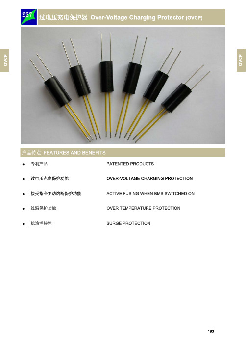
标志 Marking
商标 Trademark
过高电压充电时,电池实时电压,待电池过充后由BMS判定后切断充电电路。 Over-Voltage Charging; then BMS manages and cuts off the charging circuit.
+
-
SET 150℃ GP
OVCP 15A 36V 58
额定温度(温度保险丝)
Rated Functioning Temp. of Thermal-link
符合RoHS Compliant
型号说明 Part Number System
OVCP
15A
36V
开关电压 Threshold Voltage 工作电压 Rated Voltage 额定电流 Rated Current 类别 Type
194
过电压充电保护器 Over-Voltage Charging Protector (OVCP)
产品简介 Product Description
赛尔特的过电压充电保护器(OVCP),是一种新型的主动控制和被动控制相结合的保护器件,主要用 于锂电池组异常过电压充电保护;当充电电压达到其设定阀值电压时可同时切断输入与输出回路;也可作为 一次性主动保护装置,由电池管理系统(BMS)输出信号触发该保护器动作,实现主动保护的功能。 SET's Over Voltage Charging Protector(OVCP)is a New Device, which combines active and passive Protections for Battery Pack if abnormal over voltage charging happens. When the charging voltage reaches the given threshold value, OVCP cuts off both input and output circuits. Besides, OVCP can be an active protective device which is activated by Battery Management System(BMS).
FTLF8519F2GTL, 规格书,Datasheet 资料

Finisar Corporation October 6, 2005 Rev B
Page 1
芯天下--/
FTLF8519F2xTL 2x5 Pin SFF Product Specification – October 2005
I.
Pin Descriptions
Product Specification
2.125 Gb/s RoHS Compliant Short Wavelength 2x5 SFF Transceiver
FTLF8519F2xTL
PRODUCT FEATURES Up to 2.125 Gb/s bi-directional data links Standard 2x5 pin SFF footprint (MSA compliant) 850nm Oxide VCSEL laser transmitter Duplex LC connector RoHS compliant and Lead Free Up to 500m on 50/125µm MMF, 300m on 62.5/125µm MMF Metal enclosure, for lower EMI Single 3.3V power supply Low power dissipation <750mW Industrial operating temperature range: -40°C to 85°C Finisar’s FTLF8519F2xTL Small Form Factor (SFF) transceivers comply with the 2x5 standard package defined by the Small Form Factor Multi-Sourcing Agreement (MSA)1. They are simultaneously compatible with Gigabit Ethernet as specified in IEEE Std 802.32 and Fibre Channel FC- PI-2 Rev. 7.03. They are RoHS compliant and lead-free per Directive 2002/95/EC4 and Finisar Application Note AN-2038. PRODUCT SELECTION APPLICATIONS 1.25 Gb/s 1000Base-SX Ethernet Dual Rate 1.063/2.125 Gb/s Fibre Channel
Datasheet MLX90614 中文 数据手册 rev008

单区视场和双区视场 TO-39 封装 红外温度传感器
特性和优点
尺寸小,成本低 易集成 在极宽温度范围内工作,带出厂校准: 传感器工作温度范围:-40…+125˚C 被测目标温度范围:-70…+380˚C Ta 和 To 在 0 到 50° C 时,测量精度可达 0.5° C 高(医疗)精度校准 测量值分辨率 0.02° C 单区视场和双区视场可选 SMBus 兼容数字接口 可配置 PWM 连续输出 3V 或 5V 供电,也可使用 8…16V 供电调制 支持睡眠模式 适合不同应用领域的多种封装方式和测试方式 车用级别标准
3901090614 Rev 008
第 2ห้องสมุดไป่ตู้/ 52 页
数据手册 2013/2/28
MLX90614 系列
单区视场和双区视场 TO-39 封装 红外温度传感器
3 目录
1 功能图 ........................................................................................................................................................................................................ 1 2 概述 ......................................................................................................................................................................
东芝功放管资料

38
TIM1414-5-252
5
TIM1414-5L TIM1414-4UL NEW TIM1414-4LA TIM1414-4-252
TIM8596-4 TIM0910-4
NEW
TIM1213-4L TIM1011-4L TIM1011-4UL
NEW
36
TIM1213-4UL
TIM1011-2UL TIM8596-2 TIM0910-2 TIM1011-2L TIM1112-2
7
8
9
4
Output Power at 1dB Gain Compression (dBm)
40 Output Power at 1dB Gain Compression (W)
46
X-, Ku-band Internally Matched Power GaAs FETs/GaN HEMTs Pout vs. Frequency Map
5
■ GaN HEMTs
C-band Internally Matched Power GaN HEMT
BIAS CONDITIONS FREQUENCY BAND (GHz) 7.7-8.5
NEW 7-AA06A 7-AA04A
(Ta = 25 °C)
RF PERFORMANCE SPECIFICATIONS ABSOLUTE MAXIMUM RATINGS ELECTRICAL CHARACTERISTICS (TYP.) Tch (°C) 250 VGSoff (V) – 4.0 PACKAGE CODE IDS (@Pin = 44.0 dBm) (A) TYP. 10.0 MAX. 12.0 G✽✽ (dB) MAX. ±0.8 Tch✽ (°C) MAX. 140 50 – 10 18.0
INA149AMDREP, 规格书,Datasheet 资料

ABSOLUTE MAXIMUM RATINGS(1)
Over operating free-air temperature range, unless otherwise noted.
Supply voltage Input voltage range Common-mode and differential, 10 s Maximum Voltage on REFA and REFB Input current on any input pin(2) Output short-circuit current duration Operating temperature range Storage temperature range Junction temperature
2
PRODUCTION DATA information is current as of publication date. Products conform to specifications per the terms of the Texas Instruments standard warranty. Production processing does not necessarily include testing of all parameters.
SUPPORTS DEFENSE, AEROSPACE, AND MEDICAL APPLICATIONS
• Controlled Baseline • One Assembly/Test Site • One Fabrication Site • Available in Military (–55°C/125°C)
INA149-EP
VRF150;中文规格书,Datasheet资料

The VRF150 is a gold-metallized silicon n-channel RF power transistor de-signed for broadband commercial and military applications requiring high power and gain without compromising reliability, ruggedness, or inter-modulationdistortion.FEATURES• Improved Ruggedness V (BR)DSS = 170V• 150W with 11dB Typical Gain @ 150MHz, 50V• 150W with 18dB Typical Gain @ 30MHz, 50V • Excellent Stability & Low IMD • Common Source Con fi guration • Available in Matched Pairs• 30:1 Load VSWR Capability at Speci fi ed Operating Conditions • Nitride Passivated• Refractory Gold Metallization• High Voltage Replacement for MRF150• RoHS CompliantSymbol ParameterVRF150(MP)Unit V DSS Drain-Source Voltage170V I D Continuous Drain Current @ T C = 25°C 16A V GS Gate-Source Voltage±40V P D Total Device dissipation @ T C = 25°C 300W T STG Storage Temperature Range -65 to 150°CT JOperating Junction Temperature200Maximum Ratings All Ratings: T C =25°C unless otherwise speci fi edStatic Electrical CharacteristicsSymbol ParameterMin Typ MaxUnit V (BR)DSS Drain-Source Breakdown Voltage (V GS = 0V, I D = 100mA)170180V V DS(ON)On State Drain Voltage (I D(ON) = 10A, V GS = 10V) 2.03.0I DSS Zero Gate Voltage Drain Current (V DS = 100V, V GS = 0V) 1.0mA I GSS Gate-Source Leakage Current (V DS = ±20V, V DS = 0V) 1.0μA g fs Forward Transconductance (V DS = 10V, I D = 5A)4.5mhos V GS(TH)Gate Threshold Voltage (V DS = 10V, I D = 100mA)2.93.64.4VMicrosemi Website - 050-4936 R e v F 9-201Thermal CharacteristicsSymbol CharacteristicMin TypMax Unit R θJCJunction to Case Thermal Resistance0.60°C/WCAUTION:These Devices are Sensitive to Electrostatic Discharge. Proper Handling Procedures Should Be Followed./VRF150(MP)Dynamic CharacteristicsSymbol Parameter Test ConditionsMinTyp MaxUnitC ISS Input Capacitance V GS = 0V 420pFC oss Output CapacitanceV DS = 50V 210C rssReverse Transfer Capacitancef = 1MHz35Class A CharacteristicsSymbol Test Conditions Min Typ Max UnitG PS V DD = 50V, I DQ = 3A, P out = 150W PEP , f1 = 30MHz, f2 = 30.001MHz20dBIMD (d3)-50IMD (d9-d13)-75Functional CharacteristicsSymbol ParameterMinTyp Max Unit G PS f 1 = 30MHz, f 2 = 30.001MHz, V DD = 50V, I DQ = 250mA, P out = 150W PEP 18 dB G PS f = 150MHz, V DD = 50V, I DQ = 250mA, P out = 150W11ηD f 1 = 30MHz, f 2 = 30.001MHz, V DD = 50V, I DQ = 250mA, P out = 150W PEP 50%IMD (d3)f 1 = 30MHz, f 2 = 30.001MHz, V DD = 50V, I DQ = 250mA, P out = 150W PEP 1-32dBcIMD (d11)f 1 = 30MHz, f 2 = 30.001MHz, V DD = 50V, I DQ = 250mA, P out = 150W PEP -60ψf 1 = 30MHz, f 2 = 30.001MHz, V DD = 50V, I DQ = 250mA, P out = 150W PEP 30:1VSWR - All Phase AnglesNo Degradation in Output Power1. To MIL-STD-1311 Version A, test method 2204B, Two Tone, Reference Each ToneMicrosemi reserves the right to change, without notice, the speci fi cations and information contained herein.050-4936 R e v F 9-20101110201 10 100 250101520253035101520253035110100V DS(ON ), DRAIN-TO-SOURCE VOLTAGE (V) FIGURE 1, Output CharacteristicsI D , D R A I N C U R R E N T (A )I D , D R A I N C U R R E N T (A )VDS , DRAIN-TO-SOURCE VOLTAGE (V) FIGURE 3, Capacitance vs Drain-to-Source VoltageC , C A P A C I T A N C E (p F )V DS , DRAIN-TO-SOURCE VOLTAGE (V) FIGURE 4, Forward Safe Operating AreaI D , D R A I N C U R R E N T (V )V GS , GATE-TO-SOURCE VOLTAGE (V) FIGURE 2, Transfer CharacteristicsTypical Performance Curves/−50−45−40−35−30−25−20VRF150(MP)50-4936 R e v F 9-20100.10.20.30.40.50.60.710-510-410-3 10-2 10 1.0Z θJ C , T H E R M A L I M P E D A N C E (°C /W )RECTANGULAR PULSE DURATION (seconds)Figure 5. Maximum Effective Transient Thermal Impedance Junction-to-Case vs Pulse Duration050100150200250300P out , OUTPUT POWER (WATTS PEP)Figure 6. IMD versus P OUTI M D , I N T E R M O D U L A T I O N D I S T O R T I O N (d B )O U T P U T P O W E R (W P E P )P out , INPUT POWER (WATTS PEP)Figure 7. P OUT versus P INTypical Performance Curves/050-4936 R e v F 9-2010RFC1RFC1, C2, C8 -- Arco 463 or equivalent C3 -- 25pF, Unelco C4 -- 0.1uF, CeramicC5 -- 1.0 uF, 15 WV Tantalum C6 -- 250pF, Unelco J101C7-- 25pF, Unelco J101C9 -- Arco 262 or equivalent C10 -- 0.05uF, CeramicC11 -- 15uF, 60WV Electrolytic+ 50VDBias 0-12VRF RF OutputC2, C5, C6 - C9 -- 0.1uF SMT C3 -- 200pF ATC 700C C4 -- 15pF, ATC 700CC10 -- 10uF, 100V ElectrolyticR1, R2 -- 51 7, 1 W Carbon R3 -- 3.3 7, 1 W Carbon T1 -- 9:1 Transformer T2 -- 1:9 Transformer30 MHz test Circuit150 MHz test Circuit/050-4936 R e v F 9-2010.5” SOE Package OutlineAll Dimensions are ± .005DIMINCHES MILLIMETERS MIN MAX MIN MAX A 0.0960.99024.3925.14B0.4650.51011.8212.95C 0.2290.275 5.82 6.98D 0.2160.235 5.49 5.96E0.0840.110 2.14 2.79H0.1440.178 3.66 4.52J 0.0030.0070.080.17K 0.43511.0M45° NOM 45° NOM Q 0.1150.130 2.93 3.30R 0.2460.255 6.25 6.47U0.7200.73018.2918.54Microsemi’s products are covered by one or more of U.S. patents 4,895,810 5,045,903 5,089,434 5,182,234 5,019,522 5,262,336 6,503,786 5,256,5834,748,103 5,283,202 5,231,474 5,434,095 5,528,058 6,939,743, 7,352,045 5,283,201 5,801,417 5,648,283 7,196,634 6,664,594 7,157,886 6,939,743 7,342,262 and foreign patents. US and Foreign patents pending. All Rights Reserved.Adding MP at the end of P/N speci fi es a matched pair where V GS(TH) is matched between the two parts. V TH values are marked on the devices per the following table.Code Vth Range Code 2Vth Range A 2.900 - 2.975M 3.650 - 3.725B 2.975 - 3.050N 3.725 - 3.800C 3.050 - 3.125P 3.800 - 3.875D 3.125 - 3.200R 3.875 - 3.950E 3.200 - 3.275S 3.950 - 4.025F 3.275 - 3.350T 4.025 - 4.100G 3.350 - 3.425W 4.100 - 4.175H 3.425 - 3.500X 4.175 - 4.250J 3.500 - 3.575Y 4.250 - 4.325K3.575 - 3.650Z4.325 - 4.400V TH values are based on Microsemi measurements at datasheet conditions with an accuracy of 1.0%./分销商库存信息: MICROSEMIVRF150。
NSF14中文

元件認證指南目錄飲用水處理系統和元件認證指南章節-----------------------------------------------------------------------------------頁碼序--------------------------------------------------------------------------------------1-4 概況-----------------------------------------------------------------------------------5常見問題-----------------------------------------------------------------------------6-8 NSF標準規定-----------------------------------------------------------------------9-15 認證-----------------------------------------------------------------------------------15-18 與供應商合作-----------------------------------------------------------------------19詞彙表--------------------------------------------------------------------------------20-24 附錄A--------------------------------------------------------------------------------25附錄B--------------------------------------------------------------------------------26附錄C--------------------------------------------------------------------------------27-28 聯絡資訊-----------------------------------------------------------------------------29序NSF International(簡稱NSF)成立於1944年,為一個致力於公共衛生安全以及環境保護的機構。
datasheet_sar100_robust_gyro_sensor_ts1440_r4

VDD AVDD
VSS AVSS
References, bias and PTAT
Oscillating mass
MUX
SPI serial interface
LOAD SCLK MOSI MISO
DATASHEET
1 FEATURES o Horizontal or vertical mounting o High reliability and robustness over long lifetime o Low vibration sensitivity o High overload and shock capability (5000 g) o Butterfly balanced design for high mechanical common mode rejection o Closed-loop force feedback operation with electrostatic frequency tuning o Low bias drift o Ideal mono crystalline Si material o Wafer level sealing with controlled Q-factor o Low power o Single supply +5 VDC o Fully digital with SPI communication and on chip OTP calibration o Digitally controlled sample rate up to 2000 SPS o Bandwidth defined by built in 4th order digital LP filter o Intrinsic continuous diagnostic monitoring o Temperature sensor o No external components required
- 1、下载文档前请自行甄别文档内容的完整性,平台不提供额外的编辑、内容补充、找答案等附加服务。
- 2、"仅部分预览"的文档,不可在线预览部分如存在完整性等问题,可反馈申请退款(可完整预览的文档不适用该条件!)。
- 3、如文档侵犯您的权益,请联系客服反馈,我们会尽快为您处理(人工客服工作时间:9:00-18:30)。
164R X F线绕熔断电阻器(RXF)是将电阻丝绕在瓷基体上再经过绝缘封装处理而成的一类电阻器。
正常工作时起固定电阻器作用,当电路过载时可以在规定时间内断开,作为电路保护元件使用。
赛尔特的线绕熔断电阻器体积小,性能优异,已取得UL ,cUL ,CQC ,VDE 认证,并满足RoHS ,REACH 环保要求。
Fusible Wirewound Resistor(RXF) is a type of resistor, which is made by a resistive element wound on a ceramic core, then the core is wrapped by insulation coating. It works as a fixed resistor in normal operation, and designed to open under the over load condition, as a Protective Component. SET’s RXF products are attractive owing to their Miniaturized Size and Superior Properties and they have already been approved by UL, cUL, CQC, VDE. They also meet the requirements of RoHS, REACH. 结构图标志 Marking绝缘涂层 Insulation Coating电阻丝 Element瓷基体Ceramic Core电极帽 Cap引线 Lead Wire色环 Color Rings第一位有效数字 The First Number 第二位有效数字 The Second Number 倍率 Multiple 精度 Tolerances 功率 Power (W)黑 Black 0 0 100 — 1/2棕 Brown 1 1 101 — —红 Red 2 2 102 G: ±2% —橙 Orange 3 3 103 — —黄 Yellow 4 4 104 — 2绿 Green 5 5 105 — —蓝 Blue 6 6 106 — —紫 Purple 7 7 107 — —灰 Grey 8 8 108 — —白 White 9 9 109 — 1金 Gold — — 10-1 J: ±5% —银 Silver — — 10-2 K: ±10% —颜色 Color 165R X F 术语 Glossary of Terms对于电阻器的预定用途来说,降低其使用性的可看得见的损伤。
Damage, perceptible with suitable magnification, which is likely to affect the usability of the component for its intended purpose.在70℃环境温度下进行耐久性试验,阻值变化不超过该试验的允许值时所允许的最大功耗。
Maximum permissible dissipation at an ambient temperatureof 70℃ under the conditions of the test endurance at the rated temperature 70℃ and of the respective acceptance criteria. 两个规定温度间的阻值相对变化除以产生这个变化的温度差。
Relative variation of resistance between two given tempera-tures divided by the difference in the temperature producing it. 相对于基准温度20℃,在类别温度之间规定的温度范围内产生的阻值最大可逆变化。
The maximum reversible change of resistance happens between the given temperatures, relative to the basic tem-perature 20℃. 用标称阻值和额定功耗乘积的平方根计算出来的直流电压或交流电压有效值。
D.C. or A.C. r.m.s. voltage calculated from the square root of the product of the rated resistance and the rated dissipation.对电阻器施加规定的过负荷时,阻值显著增大;使流过电阻器的电流下降到最初试验电流的1/50以下时称为熔断,电阻器从加上规定的过负荷时到发生熔断时所需的时间称为熔断时间。
这种性能称为熔断特性。
When applied overload , the resistor’s resistance is signifi-cantly increased, and the current through the resistor dropsbelow 1/50 of the initial test current. The time from being ap-plied overload to resistor fusing is fusing time, and this per-formance is called fusing characteristics .它是由电阻丝绕于耐温绝缘瓷棒上所构成的一种电阻器,当通过它的电流超过预定值时,能在预定的时间切断电流。
熔断电阻具有不可恢复性。
A resistor which is generally made by winding resistive wire around ceramic core intended to interrupt a current flow at a predetermined time when the current passing through itexceeds a predetermined value. It is nonrenewable. 电阻器设计所确定的,通常在电阻器上标出的阻值。
Resistance value for which the resistor has been designed, and which is generally used for denomination of the resistor. RXF21 SC 4R7 J — T 60 M 01流水号Serial NO.类别 Type 额定功率 Rated Power (W) A: 1/2 SB: 1 SC: 2 精度 Tolerances(%) G: ±2 J: ±5 K: ±10 标称电阻值 Rated Resistance (Ω) R47=0.47 4R7=4.7 47R=47 电阻温度系数 Temperature Coefficient of Resistance(PPM/℃)M: ±350T: 3000~5000包装方式 Packaging T: 编带Taping B: 散装 Bulk产品总长 Total Length (mm) 607290 166R X F 关键特性 Key Features 额定 功率Rated Power(W)ΦD Φd L a L1 1/2 3.3±0.5 0.56±0.05 60±2 9±1 1 3.3±0.5 0.56±0.05 60±2 9±1 2 4.4±0.5 0.70±0.05 60±211±1 L225±225±225±2系列 Series RXF21A RXF21SB RXF21SC 应用领域 Applications● 充电器Adapter● 开关电源Switched-Mode Power Supply(SMPS) ● LED 灯具LED Lamp● 电阻温度系数(M: ±350 PPM/℃) Temperature Coefficient of Resistance (M:±350 PPM /℃) ● 耐热性好、负荷功率大 Good Heat Durability, High Load Power ● 不燃性,重量轻 Incombustibility, Light Weight ● 抗浪涌特性Surge Protection ● 环保型产品RoHS & REACH Complianta :“L ”可根据需求定制。
“L” Can be customized as required.尺寸 Dimensions (mm) 型号 Model 额定功率 Rated Power (W) 阻值范围 Resistance Range(Ω)精度 Tolerances (%) 使用温度范围OperatingTemperature Range (℃)认证信息 Agency Approvals 环境状态Environmental StatusUL cUL CQC VDE RoHS REACHRXF21Axxxx-xxx M 1/2 0.27~30 ± 5, ±10 -55~+155 ● ● ● ● ● RXF21SBxxxx-xxx M 1 0.47~51 ± 5, ±10 -55~+155 ● ● ● ● ● ● RXF21SCxxxx-xxx M 2 3~68 ± 5, ±10 -55~+155 ● ● ● ● ● ● 技术参数 Specifications备注:可根据客户要求订制无感线绕电阻。
Remark: Non-inductive resistor can be customized as required.安规认证 Agency Approvals ● CQC: CQC10001049758 CQC10001049759 CQC10001049760 ● VDE: 40035527 ● UL/cUL: E324712 ● UL 1412● GB/T 5729● GB/T 17626.5● IEC 60115● SJ 2865执行标准 Designed to StandardsD L1 L2Ld167RX F(仅供参考 Reference)额定功率降额曲线 Rated Power Derating Curve型号 Model 额定功率 Rated Power (W) 雷击浪涌电压Max. Surge Protection (kV) 应用领域ApplicationsRXF21SB2R2J-xxxM 1 2.7RXF21SB4R7J-xxxM 1 2.5RXF21SB6R8J-xxxM 1 3.0RXF21SB10RJ-xxxM 1 2.7RXF21SB12RJ-xxxM 1 2.3RXF21SB20RJ-xxxM 1 2.2 RXF21SB33RJ-xxxM 1 2.0 RXF21SB50RJ-xxxM 1 1.7 RXF21SC2R2J-xxxM 2 3.5 RXF21SC4R7J-xxxM 2 3.5RXF21SC6R8J-xxxM 2 3.8RXF21SC10RJ-xxxM 2 3.7RXF21SC12RJ-xxxM 2 3.5RXF21SC20RJ-xxxM 2 3.7● 充电器Adapter● 开关电源Switched-Mode Power Supply(SMPS)● LED 灯具LED LampRXF21SB(1 W) 熔断时间 O p e n in gT i m e (s ) 额定功率倍率 Multiples of Rated Power RXF21SC(2 W)熔断时间Openi ng Ti me(s)额定功率倍率 Multiples of Rated Power RXF21A(1/2 W) 熔断时间 O p e n in g T i m e (s ) 额定功率倍率 Multiples of Rated Power 环境温度 Ambient Temperature (℃)额定功率百分比 P e r c e n t a geo f Rat e dPo we r(%) -60 -30 0 30 60 90 120 150 180 210 240 270 300-55 70 155 27510080604020 0168R X F 测试项目 Test Items 测试条件 Test Conditions 性能要求 Performance Requirements 参考标准 Standards电阻温度系数 Temperature Coeffi-cient of Resistance (TCR)R 1:25℃下测得的电阻, R 2:125℃下测得的电阻T 1为25℃, T 2为125℃ R 1: Resistance Value at 25℃R 2: Resistance Value at 125℃T 1: 25℃, T 2:125℃±350 PPM/℃ ·IEC 60115·GB/T 5729短时间过载 Short-Time Overload 额定电压的2.5倍, 5秒 2.5 U r , 5 s 无可见损伤,标志清楚No Visible Damage and the Marking Shall be Legible ∆R ≤ ( 1%R + 0.05 Ω ) ·IEC 60115 ·GB/T 5729·SJ 2865温度循环 Temperature Cycle -55℃: 30分, 室温:10~15分钟+85℃: 30分, 室温:10~15分钟,5次循环 -55℃: 30 min, Room Temp.:10 to 15 min +85℃: 30 min, Room Temp.:10 to 15 min 5 Cycles∆R ≤ ( 1%R + 0.05 Ω )·IEC 60115 ·GB/T 5729·IEC 6006870℃耐久性 Endurance at 70℃ 在70℃ ± 2℃ ,额定电压1.5小时导通,0.5小时关断, 持续1000小时Rated Voltage 1.5 h ON, 0.5 h OFF at 70℃ or 1000 h 无可见损伤,标志清楚No Visible Damage and The Marking Shall be Legible ∆R ≤ ( 5%R + 0.1 Ω)·IEC 60115·GB/T 5729耐焊接热 Resistance toSoldering Heat 在350℃ ±10℃锡炉中浸入10秒 ±1秒 Immerge Into the 350℃ ±10℃ Tin Stove for 10 s ±1 s ∆R ≤ (1%R + 0.05 Ω) ·IEC 60115 ·GB/T 5729·SJ 2865可焊性 Solderability 在260℃ ± 5℃锡炉中浸入2.5秒± 0.5秒 Immerge Into the 260℃±5℃ Tin Stove for 2.5 s ±0.5 s 引线焊锡面积覆盖率≥95%The Soldering Area is No Less Than 95% ·IEC 60115·GB/T 5729系列 Series 额定功率 Rated Power (W) 尺寸Dimensions (mm) 数量Quantity(pcs)L W H RXF21A 1/2 400±5 275±5 20000RXF21SB 1 20000RXF21SC 2 220±5 10000240±5 LH W (外包装 Outer Packaging)系列 Series 额定功率 Rated Power(W) 尺寸Dimensions (mm) 数量Quantity(pcs)L W H RXF21A 1/2 255±5 76±5 2000RXF21SB 1 2000 RXF21SC 2 98±5 1000108±5 L (内包装 Inner Packaging) H W 169R X F 关键特性 Key Features 应用领域 Applicationsa:“L ”可根据需求定制。