LP2951-50D中文资料
LP2951-50DR中文资料

• LP2951 Only (8-Pin Package) – Fixed- or Adjustable-Output Voltages: 5 V/ADJ, 3.3 V/ADJ, and 3 V/ADJ
– Low-Voltage Error Signal on Falling Output
ORDERING INFORMATION(1)
TA –40°C to 125°C
VOUT (NOM)
3V
3.3 V
5V ADJ
PACKAGE (2)
TO-226/TO-92 – LP SOIC – D TO-226/TO-92 – LP SOIC – D TO-226/TO-92 – LP SOIC – D SOIC-D
Please be aware that an important notice concerning availability, standard warranty, and use in critical applications of Texas Instruments semiconductor products and disclaimers thereto appears at the end of this data sheet.
– 1.4% at 25°C – 2% Over Temperature • Can Be Used as a Regulator or Reference
• Stable With Low ESR (>12 mΩ) Capacitors • Current- and Thermal-Limiting Features • LP2950 Only (3-Pin Package)
LP2950-50LP中文资料
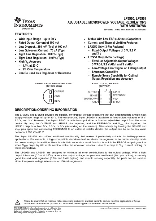
OUTPUT GND INPUT
OUTPUT 1 SENSE 2
SHUTDOWN 3 GND 4
8 INPUT 7 FEEDBACK 6 VTAP 5 ERROR
DESCRIPTION/ORDERING INFORMATION
The LP2950 and LP2951 devices are bipolar, low-dropout voltage regulators that can accommodate a wide input supply-voltage range of up to 30 V. The easy-to-use, 3-pin LP2950 is available in fixed-output voltages of 5 V, 3.3 V, and 3 V. However, the 8-pin LP2951 is able to output either a fixed or adjustable output from the same device. By tying the OUTPUT and SENSE pins together, and the FEEDBACK and VTAP pins together, the LP2951 outputs a fixed 5 V, 3.3 V, or 3 V (depending on the version). Alternatively, by leaving the SENSE and VTAP pins open and connecting FEEDBACK to an external resistor divider, the output can be set to any value between 1.235 V to 30 V.
LP2985

LP2985Micropower 150mA Low-Noise Ultra Low-Dropout Regulator in SOT-23and micro SMD PackagesDesigned for Use with Very Low ESR Output CapacitorsGeneral DescriptionThe LP2985is a 150mA,fixed-output voltage regulator designed to provide ultra low-dropout and low noise in bat-tery powered applications.Using an optimized VIP ™(Vertically Integrated PNP)pro-cess,the LP2985delivers unequalled performance in all specifications critical to battery-powered designs:Dropout Voltage:Typically 300mV @150mA load,and 7mV @1mA load.Ground Pin Current:Typically 850µA @150mA load,and 75µA @1mA load.Enhanced Stability:The LP2985is stable with output ca-pacitor ESR as low as 5m Ω,which allows the use of ceramic capacitors on the output.Sleep Mode:Less than 1µA quiescent current when ON/OFF pin is pulled low.Smallest Possible Size:SOT-23and micro SMD packages use absolute minimum board space.Precision Output:1%tolerance output voltages available (A grade).Low Noise:By adding a 10nF bypass capacitor,output noise can be reduced to 30µV (typical).Multiple voltage options,from 2.5V to 5.0V,are available as standard products.Consult factory for custom voltages.Featuresn Ultra low dropout voltagen Guaranteed 150mA output currentn Smallest possible size (SOT-23,micro SMD package)n Requires minimum external components n Stable with low-ESR output capacitor n <1µA quiescent current when shut down n Low ground pin current at all loads n Output voltage accuracy 1%(A Grade)n High peak current capabilityn Wide supply voltage range (16V max)n Low Z OUT :0.3Ωtypical (10Hz to 1MHz)n Overtemperature/overcurrent protectionn −40˚C to +125˚C junction temperature range nCustom voltages availableApplicationsn Cellular Phonen Palmtop/Laptop Computern Personal Digital Assistant (PDA)nCamcorder,Personal Stereo,CameraBlock Diagram10014001VIP ™is a trademark of National Semiconductor Corporation.March 2004LP2985Micropower 150mA Low-Noise Ultra Low-Dropout Regulator in SOT-23and micro SMD Packages©2004National Semiconductor Corporation Basic Application Circuit10014002*ON/OFF input must be actively terminated.Tie to V IN if this function is not to be used.**Minimum capacitance is shown to ensure stability (may be increased without limit).Ceramic capacitor required for output (see Application Hints).***Reduces output noise (may be omitted if application is not noise critical).Use ceramic or film type with very low leakage current (see Application Hints).Connection Diagrams5-Lead Small Outline Package (M5)micro SMD,5Bump Package (BPA05,TPA05&BLA05)10014003Top ViewSee NS Package Number MF05A For ordering information see Table 110014046Note:The actual physical placement of the package marking will vary from part to part.Package marking contains date code and lot traceabilityinformation,and will vary considerably.Package marking does not correlate to device type.Top ViewSee NS Package Number BPA05,TPA05&BLA05Pin DescrptionNamePin NumberFunctionSOT-23micro SMDV IN 1C3Input VoltageGND 2A1Common Ground (device substrate)ON/OFF 3A3Logic high enable inputBYPASS 4B2Bypass capacitor for low noise operation V OUT5C1Regulated output voltageL P 2985 2Ordering InformationTABLE1.Package Marking and Ordering InformationOutput Voltage(V)Grade Order Information PackageMarkingSupplied as:5-Lead Small Outline Package(M5)For output voltages≤2.3V,refer to LP2985LV datasheet.2.5A LP2985AIM5X-2.5LAUA3000Units on Tape and Reel2.5A LP2985AIM5-2.5LAUA1000Units on Tape and Reel2.5STD LP2985IM5X-2.5LAUB3000Units on Tape and Reel2.5STD LP2985IM5-2.5LAUB1000Units on Tape and Reel2.6A LP2985AIM5X-2.6LCEA3000Units on Tape and Reel2.6A LP2985AIM5-2.6LCEA1000Units on Tape and Reel2.6STD LP2985IM5X-2.6LCEB3000Units on Tape and Reel2.6STD LP2985IM5-2.6LCEB1000Units on Tape and Reel2.7A LP2985AIM5X-2.7LALA3000Units on Tape and Reel2.7A LP2985AIM5-2.7LALA1000Units on Tape and Reel2.7STD LP2985IM5X-2.7LALB3000Units on Tape and Reel2.7STD LP2985IM5-2.7LALB1000Units on Tape and Reel2.8A LP2985AIM5X-2.8L0KA3000Units on Tape and Reel2.8A LP2985AIM5-2.8L0KA1000Units on Tape and Reel2.8STD LP2985IM5X-2.8L0KB3000Units on Tape and Reel2.8STD LP2985IM5-2.8L0KB1000Units on Tape and Reel2.9A LP2985AIM5X-2.9LAXA3000Units on Tape and Reel2.9A LP2985AIM5-2.9LAXA1000Units on Tape and Reel2.9STD LP2985IM5X-2.9LAXB3000Units on Tape and Reel2.9STD LP2985IM5-2.9LAXB1000Units on Tape and Reel3.0A LP2985AIM5X-3.0L0OA3000Units on Tape and Reel3.0A LP2985AIM5-3.0L0OA1000Units on Tape and Reel3.0STD LP2985IM5X-3.0L0OB3000Units on Tape and Reel3.0STD LP2985IM5-3.0L0OB1000Units on Tape and Reel3.1A LP2985AIM5X-3.1L0PA3000Units on Tape and Reel3.1A LP2985AIM5-3.1L0PA1000Units on Tape and Reel3.1STD LP2985IM5X-3.1L0PB3000Units on Tape and Reel3.1STD LP2985IM5-3.1L0PB1000Units on Tape and Reel3.2A LP2985AIM5X-3.2L0QA3000Units on Tape and Reel3.2A LP2985AIM5-3.2L0QA1000Units on Tape and Reel3.2STD LP2985IM5X-3.2L0QB3000Units on Tape and Reel3.2STD LP2985IM5-3.2L0QB1000Units on Tape and Reel3.3A LP2985AIM5X-3.3L0RA3000Units on Tape and Reel3.3A LP2985AIM5-3.3L0RA1000Units on Tape and Reel3.3STD LP2985IM5X-3.3L0RB3000Units on Tape and Reel3.3STD LP2985IM5-3.3L0RB1000Units on Tape and Reel3.5A LP2985AIM5X-3.5LAIA3000Units on Tape and Reel3.5A LP2985AIM5-3.5LAIA1000Units on Tape and Reel3.5STD LP2985IM5X-3.5LAIB3000Units on Tape and Reel3.5STD LP2985IM5-3.5LAIB1000Units on Tape and Reel3.6A LP2985AIM5X-3.6L0SA3000Units on Tape and Reel3.6A LP2985AIM5-3.6L0SA1000Units on Tape and Reel3.6STD LP2985IM5X-3.6L0SB3000Units on Tape and Reel3.6STD LP2985IM5-3.6L0SB1000Units on Tape and Reel3.8A LP2985AIM5X-3.8L0YA3000Units on Tape and ReelLP29853Ordering Information(Continued)TABLE 1.Package Marking and Ordering Information (Continued)Output Voltage (V)Grade Order Information Package Marking Supplied as:3.8A LP2985AIM5-3.8L0YA 1000Units on Tape and Reel 3.8STD LP2985IM5X-3.8L0YB 3000Units on Tape and Reel 3.8STD LP2985IM5-3.8L0YB 1000Units on Tape and Reel4.0A LP2985AIM5X-4.0L0TA 3000Units on Tape and Reel 4.0A LP2985AIM5-4.0L0TA 1000Units on Tape and Reel 4.0STD LP2985IM5X-4.0L0TB 3000Units on Tape and Reel 4.0STD LP2985IM5-4.0L0TB 1000Units on Tape and Reel 4.5A LP2985AIM5X-4.5LA7A 3000Units on Tape and Reel 4.5A LP2985AIM5-4.5LA7A 1000Units on Tape and Reel 4.5STD LP2985IM5X-4.5LA7B 3000Units on Tape and Reel 4.5STD LP2985IM5-4.5LA7B 1000Units on Tape and Reel 4.7A LP2985AIM5X-4.7LAJA 3000Units on Tape and Reel 4.7A LP2985AIM5-4.7LAJA 1000Units on Tape and Reel 4.7STD LP2985IM5X-4.7LAJB 3000Units on Tape and Reel 4.7STD LP2985IM5-4.7LAJB 1000Units on Tape and Reel 4.8A LP2985AIM5X-4.8LAKA 3000Units on Tape and Reel 4.8A LP2985AIM5-4.8LAKA 1000Units on Tape and Reel 4.8STD LP2985IM5X-4.8LAKB 3000Units on Tape and Reel 4.8STD LP2985IM5-4.8LAKB 1000Units on Tape and Reel5.0A LP2985AIM5X-5.0L0UA 3000Units on Tape and Reel 5.0A LP2985AIM5-5.0L0UA 1000Units on Tape and Reel 5.0STD LP2985IM5X-5.0L0UB 3000Units on Tape and Reel 5.0STD LP2985IM5-5.0L0UB 1000Units on Tape and Reel 5.3A LP2985AIM5X-5.3LFYA 3000Units on Tape and Reel 5.3A LP2985AIM5-5.3LFYA 1000Units on Tape and Reel 5.3STD LP2985IM5X-5.3LFYB 3000Units on Tape and Reel 5.3STD LP2985IM5-5.3LFYB 1000Units on Tape and Reel6.1A LP2985AIM5X-6.1LF6A 3000Units on Tape and Reel 6.1A LP2985AIM5-6.1LF6A 1000Units on Tape and Reel 6.1STD LP2985IM5X-6.1LF6B 3000Units on Tape and Reel 6.1STD LP2985IM5-6.1LF6B 1000Units on Tape and Reel 12(Note 11)A LP2985AIM5X-12LH1A 3000Units on Tape and Reel 12(Note 11)A LP2985AIM5-12LH1A 1000Units on Tape and Reel 12(Note 11)STD LP2985IM5X-12LH1B 3000Units on Tape and Reel 12(Note 11)STDLP2985IM5-12LH1B1000Units on Tape and Reelmicro SMD,5Bump Package (BPA05-170µm ball)2.4A LP2985AIBP-2.4250Units on Tape and Reel 2.4A LP2985AIBPX-2.43000Units on Tape and Reel 2.4STD LP2985IBP-2.4250Units on Tape and Reel 2.4STD LP2985IBPX-2.43000Units on Tape and Reel 2.5A LP2985AIBP-2.5250Units on Tape and Reel 2.5A LP2985AIBPX-2.53000Units on Tape and Reel 2.5STD LP2985IBP-2.5250Units on Tape and Reel 2.5STDLP2985IBPX-2.53000Units on Tape and ReelL P 29854Ordering Information(Continued)TABLE1.Package Marking and Ordering Information(Continued)Output Voltage(V)Grade Order Information PackageMarkingSupplied as:2.6A LP2985AIBP-2.6250Units on Tape and Reel2.6A LP2985AIBPX-2.63000Units on Tape and Reel2.6STD LP2985IBP-2.6250Units on Tape and Reel2.6STD LP2985IBPX-2.63000Units on Tape and Reel2.8A LP2985AIBP-2.8250Units on Tape and Reel2.8A LP2985AIBPX-2.83000Units on Tape and Reel2.8STD LP2985IBP-2.8250Units on Tape and Reel2.8STD LP2985IBPX-2.83000Units on Tape and Reel2.9A LP2985AIBP-2.9250Units on Tape and Reel2.9A LP2985AIBPX-2.93000Units on Tape and Reel2.9STD LP2985IBP-2.9250Units on Tape and Reel2.9STD LP2985IBPX-2.93000Units on Tape and Reel3.0A LP2985AIBP-3.0250Units on Tape and Reel3.0A LP2985AIBPX-3.03000Units on Tape and Reel3.0STD LP2985IBP-3.0250Units on Tape and Reel3.0STD LP2985IBPX-3.03000Units on Tape and Reel3.3A LP2985AIBP-3.3250Units on Tape and Reel3.3A LP2985AIBPX-3.33000Units on Tape and Reel3.3STD LP2985IBPX-3.3250Units on Tape and Reel3.3STD LP2985IBPX-3.33000Units on Tape and Reel3.6A LP2985AIBP-3.6250Units on Tape and Reel3.6A LP2985AIBPX-3.63000Units on Tape and Reel3.6STD LP2985IBP-3.6250Units on Tape and Reel3.6STD LP2985IBPX-3.63000Units on Tape and Reel4.0A LP2985AIBP-4.0250Units on Tape and Reel4.0A LP2985AIBPX-4.03000Units on Tape and Reel4.0STD LP2985IBP-4.0250Units on Tape and Reel4.0STD LP2985IBPX-4.03000Units on Tape and Reel5.0A LP2985AIBP-5.0250Units on Tape and Reel5.0A LP2985AIBPX-5.03000Units on Tape and Reel5.0STD LP2985IBP-5.0250Units on Tape and Reel5.0STD LP2985IBPX-5.03000Units on Tape and Reelmicro SMD,5Bump Package(TPA05-170µm ball)2.5A LP2985AITP-2.5250Units on Tape and Reel2.5A LP2985AITPX-2.53000Units on Tape and Reel2.5STD LP2985ITP-2.5250Units on Tape and Reel2.5STD LP2985ITPX-2.53000Units on Tape and Reel2.7A LP2985AITP-2.7250Units on Tape and Reel2.7A LP2985AITPX-2.73000Units on Tape and Reel2.7STD LP2985ITP-2.7250Units on Tape and Reel2.7STD LP2985ITPX-2.73000Units on Tape and Reel2.8A LP2985AITP-2.8250Units on Tape and Reel2.8A LP2985AITPX-2.83000Units on Tape and Reel2.8STD LP2985ITP-2.8250Units on Tape and Reel2.8STD LP2985ITPX-2.83000Units on Tape and Reel5.0A LP2985AITP-5.0250Units on Tape and Reel5.0A LP2985AITPX-5.03000Units on Tape and ReelLP29855Ordering Information(Continued)TABLE 1.Package Marking and Ordering Information (Continued)Output Voltage (V)Grade Order Information Package MarkingSupplied as:5.0STD LP2985ITP-5.0250Units on Tape and Reel 5.0STD LP2985ITPX-5.03000Units on Tape and Reel micro SMD,5Bump Package (BLA05-300µm ball)2.85A LP2985AIBL-285250Units on Tape and Reel 2.85A LP2985AIBLX-2853000Units on Tape and Reel 2.85STD LP2985IBL-285250Units on Tape and Reel 2.85STD LP2985IBLX-2853000Units on Tape and Reel3.0A LP2985AIBL-3.0250Units on Tape and Reel 3.0A LP2985AIBLX-3.03000Units on Tape and Reel 3.0STD LP2985IBL-3.0250Units on Tape and Reel 3.0STD LP2985IBLX-3.03000Units on Tape and Reel 3.3A LP2985AIBL-3.3250Units on Tape and Reel 3.3A LP2985AIBLX-3.33000Units on Tape and Reel 3.3STD LP2985IBL-3.3250Units on Tape and Reel 3.3STDLP2985IBLX-3.33000Units on Tape and ReelL P 2985 6Absolute Maximum Ratings (Note 1)If Military/Aerospace specified devices are required,please contact the National Semiconductor Sales Office/Distributors for availability and specifications.Storage Temperature Range −65˚C to +150˚C Operating Junction Temperature Range−40˚C to +125˚CLead Temp.(Soldering,5sec.)260˚C ESD Rating (Note 2)2kVPower Dissipation (Note 3)Internally LimitedInput Supply Voltage (Survival)−0.3V to +16V Input Supply Voltage (Operating) 2.5V to +16V Shutdown Input Voltage (Survival)−0.3V to +16V Output Voltage (Survival,(Note 4))−0.3V to +9V I OUT (Survival)Short Circuit Protected Input-Output Voltage (Survival,−0.3V to +16V(Note 5))Electrical Characteristics (Note 10)Limits in standard typeface are for T J =25˚C.and limits in boldface type apply over the full operating temperature range.Un-less otherwise specified:V IN =V O (NOM)+1V,I L =1mA,C IN =1µF,C OUT =4.7µF,V ON/OFF =2V.Symbol Parameter ConditionsTypLP2985AI-X.XLP2985I-X.X Units(Note 6)(Note 6)Min Max Min Max ∆V OOutput Voltage ToleranceI L =1mA−1.0 1.0−1.5 1.5%V NOM 1mA ≤I L ≤50mA −1.5 1.5−2.5 2.5−2.5 2.5−3.5 3.51mA ≤I L ≤150mA−2.5 2.5−3.0 3.0−3.53.5−4.04.0Output Voltage V O (NOM)+1V ≤V IN ≤16V0.0070.0140.014%/V Line Regulation0.0320.032V IN –V ODropout Voltage (Note 7)I L =0133mV 55I L =1mA 710101515I L =10mA 4060609090I L =50mA 120150*********I L =150mA280350350575575I GNDGround Pin Current (Note 11)I L =0659595µA 125125I L =1mA 75110110170170I L =10mA 120220220400400I L =50mA 35060060010001000I L =150mA 8501500150025002500V ON/OFF <0.3V 0.010.80.8V ON/OFF <0.15V0.0522V ON/OFF ON/OFF Input Voltage (Note 8)High =O/P ON 1.4 1.61.6V Low =O/P OFF 0.550.150.15I ON/OFFON/OFF Input CurrentV ON/OFF =00.01−2−2µA V ON/OFF =5V51515LP29857Electrical Characteristics (Note 10)(Continued)Limits in standard typeface are for T J =25˚C.and limits in boldface type apply over the full operating temperature range.Un-less otherwise specified:V IN =V O (NOM)+1V,I L =1mA,C IN =1µF,C OUT =4.7µF,V ON/OFF =2V.SymbolParameter ConditionsTypLP2985AI-X.XLP2985I-X.X Units(Note 6)(Note 6)MinMaxMinMaxe nOutput Noise BW =300Hz to 50kHz,Voltage (RMS)C OUT =10µF 30µVC BYPASS =10nFRipple Rejectionf =1kHz,C BYPASS =10nF 45dB C OUT =10µFI O (SC)Short Circuit Current R L =0(Steady State)400mA (Note 9)I O (PK)Peak Output CurrentV OUT ≥V o (NOM)−5%350mANote 1:“Absolute Maximum Ratings”indicate limits beyond which damage to the component may occur.Electrical specifications do not apply when operating the device outside of its rated operating conditions.Note 2:The ESD rating of pins 3and 4for the SOT-23package,or pins 5and 2for the micro SMD package,is 1kV.Note 3:The maximum allowable power dissipation is a function of the maximum junction temperature,T J (MAX),the junction-to-ambient thermal resistance,θJ-A ,and the ambient temperature,T A .The maximum allowable power dissipation at any ambient temperture is calculated using:Where the value of θJ-A for the SOT-23package is 220˚C/W in a typical PC board mounting and the micro SMD package is 225˚C/W.Exceeding the maximum allowable dissipation will cause excessive die temperature,and the regulator will go into thermal shutdown.Note 4:For 12V option,output voltage survival:-0.3to +16V.If used in a dual-supply system where the regulator load is returned to a negative supply,the LP2985output must be diode-clamped to ground.Note 5:The output PNP structure contains a diode between the V IN to V OUT terminals that is normally reverse-biased.Reversing the polarity from V IN to V OUT will turn on this diode.Note 6:Limits are 100%production tested at 25˚C.Limits over the operating temperature range are guaranteed through correlation using Statistical Quality Control (SQC)methods.The limits are used to calculate National’s Average Outgoing Quality Level (AOQL).Note 7:Dropout voltage is defined as the input to output differential at which the output voltage drops 100mV below the value measured with a 1V differential.Note 8:The ON/OFF input must be properly driven to prevent possible misoperation.For details,refer to Application Hints.Note 9:The LP2985has foldback current limiting which allows a high peak current when V OUT >0.5V,and then reduces the maximum output current as V OUT is forced to ground (see Typical Performance Characteristics curves).Note 10:Exposing the micro SMD device to direct sunlight will cause misoperation.See Application Hints for additional information.Note 11:For 12V option,add 50µA to all ON state quiescent current values.L P 2985 8Typical Performance CharacteristicsUnless otherwise specified:C IN =1µF,C OUT =4.7µF,V IN =V OUT (NOM)+1,T A =25˚C,ON/OFF pin is tied to V IN .V OUT vs TemperatureShort-Circuit Current1001400810014009Short-Circuit Current Short Circuit Current vs Output Voltage1001401010014011Ripple Rejection Ripple Rejection1001401310014014LP29859Typical Performance Characteristics Unless otherwise specified:C IN =1µF,C OUT =4.7µF,V IN =V OUT (NOM)+1,T A =25˚C,ON/OFF pin is tied to V IN .(Continued)Ripple RejectionRipple Rejection1001401510014016Ripple Rejection Ripple Rejection1001401710014018Ripple Rejection Ripple Rejection1001401910014023L P 2985 10Typical Performance Characteristics Unless otherwise specified:C IN =1µF,C OUT =4.7µF,V IN =V OUT (NOM)+1,T A =25˚C,ON/OFF pin is tied to V IN .(Continued)Ripple Rejection Output Impedance vs Frequency1001402210014020Output Impedance vs Frequency Output Noise Density1001402110014024Output Noise Density Ground Pin vs Load Current1001402510014026LP2985Typical Performance Characteristics Unless otherwise specified:C IN =1µF,C OUT =4.7µF,V IN =V OUT (NOM)+1,T A =25˚C,ON/OFF pin is tied to V IN .(Continued)Dropout Voltage vs Temperature Input Current vs Pin1001402710014029GND Pin Current vs Temperature Instantaneous Short Circuit Current1001403010014031Load Transient Response Load Transient Response1001403210014033L P 2985Typical Performance Characteristics Unless otherwise specified:C IN =1µF,C OUT =4.7µF,V IN =V OUT (NOM)+1,T A =25˚C,ON/OFF pin is tied to V IN .(Continued)Load Transient Response Line Transient Response1001403410014035Line Transient Response Line Transient Response1001403610014037Line Transient Response Turn-On Time1001403810014039LP2985Typical Performance Characteristics Unless otherwise specified:C IN =1µF,C OUT =4.7µF,V IN =V OUT (NOM)+1,T A =25˚C,ON/OFF pin is tied to V IN .(Continued)Turn-On Time Turn-On Time1001404010014041Turn-On Time10014042L P 2985Application HintsEXTERNAL CAPACITORSLike any low-dropout regulator,the LP2985requires external capacitors for regulator stability.These capacitors must be correctly selected for good performance.Input CapacitorAn input capacitor whose capacitance is≥1µF is required between the LP2985input and ground(the amount of ca-pacitance may be increased without limit).This capacitor must be located a distance of not more than1 cm from the input pin and returned to a clean analog ground. Any good quality ceramic,tantalum,or film capacitor may be used at the input.Important:Tantalum capacitors can suffer catastrophic fail-ure due to surge current when connected to a low-impedance source of power(like a battery or very large capacitor).If a Tantalum capacitor is used at the input,it must be guaranteed by the manufacturer to have a surge current rating sufficient for the application.There are no requirements for ESR on the input capacitor, but tolerance and temperature coefficient must be consid-ered when selecting the capacitor to ensure the capacitance will be≥1µF over the entire operating temperature range. Output CapacitorThe LP2985is designed specifically to work with ceramic output capacitors,utilizing circuitry which allows the regula-tor to be stable across the entire range of output current with an output capacitor whose ESR is as low as5mΩ.It may also be possible to use Tantalum or film capacitors at the output,but these are not as attractive for reasons of size and cost(see next section Capacitor Characteristics).The output capacitor must meet the requirement for mini-mum amount of capacitance and also have an ESR(equiva-lent series resistance)value which is within the stable range. Curves are provided which show the stable ESR range as a function of load current(see ESR graph below).10014007 Important:The output capacitor must maintain its ESR within the stable region over the full operating temperature range of the application to assure stability.The LP2985requires a minimum of2.2µF on the output (output capacitor size can be increased without limit).It is important to remember that capacitor tolerance and variation with temperature must be taken into consideration when selecting an output capacitor so that the minimum required amount of output capacitance is provided over the full operating temperature range.It should be noted that ceramic capacitors can exhibit large changes in capacitancewith temperature(see next section,Capacitor Characteris-tics).The output capacitor must be located not more than1cmfrom the output pin and returned to a clean analog ground.Noise Bypass CapacitorConnecting a10nF capacitor to the Bypass pin significantly reduces noise on the regulator output.It should be noted thatthe capacitor is connected directly to a high-impedance cir-cuit in the bandgap reference.Because this circuit has only a few microamperes flowing init,any significant loading on this node will cause a change inthe regulated output voltage.For this reason,DC leakagecurrent through the noise bypass capacitor must never ex-ceed100nA,and should be kept as low as possible for bestoutput voltage accuracy.The types of capacitors best suited for the noise bypass capacitor are ceramic and film.High-quality ceramic capaci-tors with either NPO or COG dielectric typically have verylow leakage.10nF polypropolene and polycarbonate film capacitors are available in small surface-mount packagesand typically have extremely low leakage current.CAPACITOR CHARACTERISTICSThe LP2985was designed to work with ceramic capacitorson the output to take advantage of the benefits they offer:for capacitance values in the2.2µF to4.7µF range,ceramicsare the least expensive and also have the lowest ESRvalues(which makes them best for eliminating high-frequency noise).The ESR of a typical 2.2µF ceramic capacitor is in the range of10mΩto20mΩ,which easilymeets the ESR limits required for stability by the LP2985.One disadvantage of ceramic capacitors is that their capaci-tance can vary with temperature.Most large value ceramic capacitors(≥2.2µF)are manufactured with the Z5U or Y5V temperature characteristic,which results in the capacitance dropping by more than50%as the temperature goes from25˚C to85˚C.This could cause problems if a2.2µF capacitor were usedon the output since it will drop down to approximately1µF athigh ambient temperatures(which could cause the LM2985to oscillate).If Z5U or Y5V capacitors are used on the output,a minimum capacitance value of4.7µF must be observed.A better choice for temperature coefficient in ceramic capaci-tors is X7R,which holds the capacitance within±15%.Un-fortunately,the larger values of capacitance are not offeredby all manufacturers in the X7R dielectric.TantalumTantalum capacitors are less desirable than ceramics for useas output capacitors because they are more expensive when comparing equivalent capacitance and voltage ratings in the1µF to4.7µF range.Another important consideration is that Tantalum capacitorshave higher ESR values than equivalent size ceramics.Thismeans that while it may be possible to find a Tantalum capacitor with an ESR value within the stable range,it wouldhave to be larger in capacitance(which means bigger andmore costly)than a ceramic capacitor with the same ESR value.LP2985Application Hints (Continued)It should also be noted that the ESR of a typical Tantalum willincrease about 2:1as the temperature goes from 25˚C downto −40˚C,so some guard band must be allowed.On/off Input OperationThe LP2985is shut off by driving the ON/OFF input low,andturned on by pulling it high.If this feature is not to be used,the ON/OFF input should be tied to V IN to keep the regulatoroutput on at all times.To assure proper operation,the signal source used to drivethe ON/OFF input must be able to swing above and belowthe specified turn-on/turn-off voltage thresholds listed in theElectrical Characteristics section under V ON/OFF .To preventmis-operation,the turn-on (and turn-off)voltage signals ap-plied to the ON/OFF input must have a slew rate which is≥40mV/µs.Caution:the regulator output voltage can not be guaranteedif a slow-moving AC (or DC)signal is applied that is in therange between the specified turn-on and turn-off voltageslisted under the electrical specification V ON/OFF (see Electri-cal Characteristics).REVERSE INPUT-OUTPUT VOLTAGEThe PNP power transistor used as the pass element in theLP2985has an inherent diode connected between the regu-lator output and input.During normal operation (where theinput voltage is higher than the output)this diode is reverse-biased.However,if the output is pulled above the input,this diodewill turn ON and current will flow into the regulator output.In such cases,a parasitic SCR can latch which will allow a high current to flow into V IN (and out the ground pin),which can damage the part.In any application where the output may be pulled above the input,an external Schottky diode must be connected from V IN to V OUT (cathode on V IN ,anode on V OUT ),to limit the reverse voltage across the LP2985to 0.3V (see Absolute Maximum Ratings).MICRO SMD MOUNTING The micro SMD package requires specific mounting tech-niques which are detailed in National Semiconductor Appli-cation Note #1112.Referring to the section Surface Mount Technology (SMT)Assembly Considerations ,it should be noted that the pad style which must be used with the 5-pin package is the NSMD (non-solder mask defined)type.For best results during assembly,alignment ordinals on the PC board may be used to facilitate placement of the micro SMD device.MICRO SMD LIGHT SENSITIVITY Exposing the micro SMD device to direct sunlight will cause misoperation of the device.Light sources such as Halogen lamps can also affect electrical performance if brought near to the device.The wavelenghts which have the most detrimental effect are reds and infra-reds,which means that the fluorescent light-ing used inside most buildings has very little effect on per-formance.A micro SMD test board was brought to within 1cm of a fluorescent desk lamp and the effect on the regu-lated output voltage was negligible,showing a deviation of less than 0.1%from nominal.L P 2985Physical Dimensions inches(millimeters)unless otherwise noted5-Lead Small Outline Package(M5)NS Package Number MF05AFor Order Numbers,refer to Table1in the“Ordering Information”section of this document.LP2985。
LP2951CMX中文资料

©2001 Fairchild Semiconductor CorporationRev. 1.0.0Features•Low Quiescent Current •Low Dropout V oltage•Low Temperature Coefficient •Tight Line and Load Regulation •Guaranteed 100mA Output Current •Internal Short Current & Thermal Limit•Error Signals of Output Dropout (8 pin Versions Only)•External Shut-down ( 8 pin Versions Only)DescriptionThe LP2951 is an adjustable micro power voltage regulator suitable for use in battery-powered systems. This regulator has various functions such as alarm which warns of a low output voltage, often due to falling batteries on the input, the external shutdown which enables the regulator to be switched on and off, current and temperature limiting.LP2951Adjustable Micro Power Voltage Regulator8-SOP1LP2951Absolute Maximum RatingsParameter Symbol Value Unit Input Supply Voltage V IN-0.3 ~ +30V Power Dissipation P D Internally Limited W Thermal Resistance Junction-Air RθJA127.5°C/W Storage Temperature Range T STG-65 ~ +150°C Operating Junction Temperature Range T OPR-40 ~ +125°C2LP29513Electrical Characteristics(Refer to the test circuit, Ta = 25 °C, unless otherwise specified, )Note :1. Output or reference voltage temperature coefficient is defined as the worst case voltage change divided by the total temperature range.2. Regulation is measured at constant junction temperature , using pulse testing with a low duty cycle.3. V ref ≤ V out ≤ (V in - 1V), 2.5V ≤ V in ≤ 28V, 100uA ≤ I L ≤ 100mA, T A ≤ T AMAX .4. Threshold and hysteresis are expressed in terms of voltage differential at the Feedback terminal below the normal reference . To express these thresholds in terms of output voltage change , multiply by the error amplifier gain = VO / VREF = (R1 + R2) / R2 .5. Vshutdown ≤ 0.6 V , V OUT =ON , Vshutdown ≥ 2.0 V, V OUT = OFF.ParameterSymbolConditionsMin.Typ.Max.UnitALL VOLTAGE OPTIONSOutput Voltage Temperature Coefficient ∆V /∆T (Note1)-50-ppm/°C Line Regulation (Note2)∆V (Vo + 1)V ≤V IN ≤28V I L = 50mA --0.4%Load Regulation (Note2)∆V 100uA ≤ I L ≤100mA --0.3%Dropout Voltage V D I L = 100uA --150mV I L = 100mA --600mV Ground Current I G I L = 100uA --140uA I L = 100mA --7mA Current LimitI CLV O = 0V110165220mA8-PIN VERSIONS ONLY Reference Voltage V REF (Note3)1.235 1.26 1.285V V REF1.225 1.26 1.295VERROR COMPARATOR Output Low Voltage V OL V IN = (Vo - 0.5)V, I OL =400uA -150400mV High Threshold Voltage V TH (Note4)2560-mV Low Threshold Voltage V TL (Note4)-75140mV HysteresisV HYS(Note4)-15-mVSHUTDOWN INPUT Shutdown Threshold Range V SD (Note5)0.6 1.3 2.0V Shutdown Input CurrentI SDV SD = 2.4V -30100uA V SD = 28V-450750uALP29514Typical Performance CharacteristicsFigure 1. Quiescent CurrentFigure 2. Dropout CharacteristicsFigure 3. Input CurrentFigure 4. Input CurrentFigure 6. Short Circuit CurrentFigure 5. Output Voltage vs. TemperatureLP2951 Typical Performance Characteristics (Continued)5LP2951Typical ApplicationCO is required between the output and ground for stability at output voltages of 5V or more. since IFB is controlled to less than 40nA, the error associated with this term is negligible in most applications.At lower output voltage, more capacitance is required. without this capacitance the part will oscillate.6LP2951 Mechanical DimensionPackageDimensions in millimeters8-SOP7LP2951Ordering InformationProduct Number Package Operationg Temperature LP2951CM8-SOP-40 ~ +125°C8LP29519LP29515/19/01 0.0m 001Stock#DSxxxxxxxx2001 Fairchild Semiconductor CorporationLIFE SUPPORT POLICYFAIRCHILD’S PRODUCTS ARE NOT AUTHORIZED FOR USE AS CRITICAL COMPONENTS IN LIFE SUPPORT DEVICES OR SYSTEMS WITHOUT THE EXPRESS WRITTEN APPROVAL OF THE PRESIDENT OF FAIRCHILD SEMICONDUCTOR CORPORATION. As used herein:1.Life support devices or systems are devices or systemswhich, (a) are intended for surgical implant into the body, or (b) support or sustain life, and (c) whose failure to perform when properly used in accordance with instructions for use provided in the labeling, can bereasonably expected to result in a significant injury of the user.2. A critical component in any component of a life supportdevice or system whose failure to perform can bereasonably expected to cause the failure of the life support device or system, or to affect its safety or effectiveness.DISCLAIMERFAIRCHILD SEMICONDUCTOR RESERVES THE RIGHT TO MAKE CHANGES WITHOUT FURTHER NOTICE TO ANY PRODUCTS HEREIN TO IMPROVE RELIABILITY, FUNCTION OR DESIGN. FAIRCHILD DOES NOT ASSUME ANYLIABILITY ARISING OUT OF THE APPLICATION OR USE OF ANY PRODUCT OR CIRCUIT DESCRIBED HEREIN; NEITHER DOES IT CONVEY ANY LICENSE UNDER ITS PATENT RIGHTS, NOR THE RIGHTS OF OTHERS.。
LP2951D中文资料

该lp2950和lp2951设备双极,低压差电压调节器,可以容纳广泛的输入电源电压范围高达30五,易于使用,lp2950引脚可在固定输出电压为5伏,3.3伏,3 V .然而,8引脚lp2951能够输出要么固定或可调的输出从同一装置。
通过捆绑的引脚输出和在一起,和反馈和vtap引脚,该lp2951输出固定的5伏,3.3伏,3伏(根据不同的版本)。
另外,离开意识vtap针开放和连接反馈到一个外部电阻分压器,其输出可设置为任何值1.235至308引脚lp2951还提供额外的功能,使它特别适用于电池供电应用程序。
例如,一个logic-compatible关机功能允许调节器被放置在待机模式功率节省。
此外,有一个内置监控复位功能的错误输出变低当输出电压下降6%的名义价值,什么原因–由于降低输入电压,电流限制,或热关断。
该lp2950和lp2951旨在尽量减少所有错误的贡献输出电压。
一个紧输出容忍(0.5%在25°丙),非常低的输出电压温度系数(20百万分之一典型),极好的线路和负载调节(0.3%和0.4%典型),和遥感能力,部分可以被用来作为无论是低功耗电压参考或百玛调节剂。
一个1-mf(钽,陶瓷,或铝)电解电容器应放在当地的输入lp2950或lp2951如果有,或将,重大阻抗之间的交流滤波器电容器和用于输入;例如,如果使用电池作为输入或如果交流滤波器电容器位于超过10了。
有没有电子自旋共振要求此电容器和电容,可以无限制增加。
与大多数进步党的,稳定的条件要求输出电容器至少有一个电容和一个电子自旋共振,在一定范围内。
³为输出电压为5伏,最低1中频是必要的。
低输出电压,调节器的闭环增益是接近单位增益和,因此,具有较低的相空间。
因此,较大的电容是需要稳定。
为输出电压为3伏和3.3伏,最低2.2中频建议。
最坏的情况下,输出电压为1.23伏(使用的版本),最低3.3中频建议。
我们可以无限制增加和提高调节器的稳定性和暂态响应。
美国Eaton公司产品说明书:Eaton Power Xpert
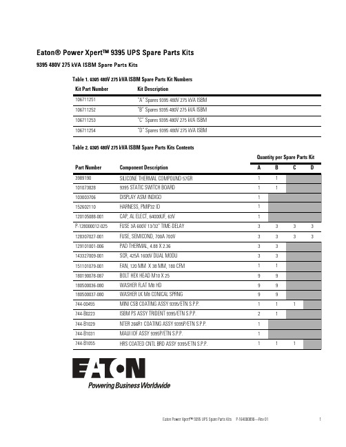
Eaton Power Xpert ™9395UPS Spare Parts Kits P-164000890—Rev 011E a t o n ®P o w e r X p e r t ™9395U P S S p a r e P a r t s K i t s9395480V 275k V A I S B M S p a r e P a r t s K i t sTable 1.9395480V 275kVA ISBM Spare Parts Kit Numbers Kit Part Number Kit Description106711251“A”Spares 9395480V 275kVA ISBM 106711252“B”Spares 9395480V 275kVA ISBM 106711253“C”Spares 9395480V 275kVA ISBM 106711254“D”Spares 9395480V 275kVA ISBMTable 2.9395480V 275kVA ISBM Spare Parts Kits ContentsQuantity per Spare Parts KitPart Number Component DescriptionA B CDP-128000012-025FUSE 3A 600V 13/32"TIME-DELAY 3333128307027-001FUSE,SEMICOND,700A 700V 33332Eaton Power Xpert ™9395UPS Spare Parts Kits P-164000890—Rev019395480V 550k V A I S B M S p a r e P a r t s K i t sTable 3.9395480V 550kVA ISBM Spare Parts Kits Kit Part Number Kit Description106711259“A”Spares 9395480V 550kVA ISBM 106711260“B”Spares 9395480V 550kVA ISBM 106711261“C”Spares 9395480V 550kVA ISBM 106711262“D”Spares 9395480V 550kVA ISBMTable 4.9395480V 550kVA ISBM Spare Parts Kits ContentsQuantity per Spare Parts KitPart Number Component Description A B CD10268203333P-128000012-025FUSE 3A 600V 13/32"TIME-DELAY 3333Eaton Power Xpert ™9395UPS Spare Parts Kits P-164000890—Rev 0139395400/480V 825k V A M S S I S B M S p a r e P a r t s K i t sTable 5.9395400/480V 825kVA MSS ISBM Spares Kits Kit Part Number Component Description106711271“A”Spares 9395400/480825kVA MSS ISBM 106711275“B”Spares 9395400/480825kVA MSS ISBM 106711279“C”Spares 9395400/480825kVA MSS ISBM 106711283“D”Spares 9395400/480825kVA MSS ISBMTable 6.9395400/480V 825kVA MSS ISBM Spare Parts Kits ContentsQuantity per Spare Parts KitPart Number Component Description A BCDP-128000012-025FUSE 3A 600V 13/32"TIME-DELAY 4666128307029-002FUSE,2000A,690V,HIGH SPEED,SQUARE BODY 6666744-B1055HRS COATED CNTL BRD ASSY 9395/ETN S.P.P.11114Eaton Power Xpert ™9395UPS Spare Parts Kits P-164000890—Rev019395400/480V 825k V A I S B M C S S S p a r e P a r t s K i t sTable 7.9395400/480V 825kVA ISBM CSS Spares Kits Kit Part Number Component Description106711273“A”Spares 9395400/480825kVA ISBM CSS 106711277“B”Spares 9395400/480825kVA ISBM CSS 106711281“C”Spares 9395400/480825kVA ISBM CSS 106711285“D”Spares 9395400/480825kVA ISBM CSSTable 8.9395400/480V 825kVA ISBM CSS Spare Parts Kits ContentsQuantity per Spare Parts KitPart Number Component Description A BCD1111129400075PAD,THERMAL INTERFACE 18181810P-128000012-025FUSE 3A 600V 13/32"TIME-DELAY121266128307029-002FUSE,2000A,690V,HIGH SPEED,SQUARE BODY 121266180500034-625M6X 25SCKT HD CAP SCR24242416744-00455MINI CSB COATING ASSY 9395/ETN S.P.P.1111744-B0223ISBM PS ASSY TRIDENT 9395/ETN S.P.P.2211744-B1055HRS COATED CNTL BRD ASSY 9395/ETN S.P.P.1111P-143000024Thyristor,SEMIKRON SKET 801819A 1800V6664Eaton Power Xpert ™9395UPS Spare Parts Kits P-164000890—Rev 0159395480V 1100k V A C S S I S B M S p a r e P a r t s K i t sTable 9.9395480V 1100kVA CSS ISBM Spares Kits Kit Part Number Component Description106711310“A”Spares 9395480825kVA ISBM CSS 106711312“B”Spares 9395480825kVA ISBM CSS 106711314“C”Spares 9395480825kVA ISBM CSS 106711316“D”Spares 9395480825kVA ISBM CSSTable 10.9395480V 1100kVA CSS ISBM Spare Parts Kits ContentsQuantity per Spare Parts KitPart Number Component Description A B CD103003706DISPLAY ASM INDIGO 1111103007183ASSY,ST SW 2000A 3321P-128000012-025FUSE 3A 600V 13/32"TIME-DELAY6566128307029-003FUSE,3000A,690V,HIGH SPEED,SQUARE BODY 6166744-00455MINI CSB COATING ASSY 9395/ETN S.P.P.1111744-B0223ISBM PS ASSY TRIDENT 9395/ETN S.P.P.4121744-B1029NTER 266R1COATING ASSY 9395P/ETN S.P.P.11116Eaton Power Xpert ™9395UPS Spare Parts Kits P-164000890—Rev019395400/480V 1100k V A M S S I S B M S p a r e P a r t s K i t sTable 11.9395400/480V 1100kVA MSS ISBM Spare Parts Kits Kit Part Number Component Description106711302“A”Spares 9395400/480V 1100kVA MSS ISBM 106711304“B”Spares 9395400/480V 1100kVA MSS ISBM 106711306“C”Spares 9395400/480V 1100kVA MSS ISBM 106711308“D”Spares 9395400/480V 1100kVA MSS ISBMTable 12.9395400/480V 1100kVA MSS ISBM Spare Parts Kits ContentsQuantity per Spare Parts KitPart Number Component Description A B CDP-128000012-022FUSE 2.25A 600V 13/32”TIME-DELAY 3333P-128000012-025FUSE 3A 600V 13/32"TIME-DELAY 4666128307029-003FUSE,3000A,690V,HIGH SPEED,SQUARE BODY 6666744-B1055HRS COATED CNTL BRD ASSY 9395/ETN S.P.P.1111Eaton Power Xpert ™9395UPS Spare Parts Kits P-164000890—Rev 0179395400V /480V U P M S p a r e P a r t K i t sTable 13.9395400/480V UPM Spare Parts Kits Kit Part Number Component Description106711267“A”9395400/480V UPM Spare Parts Kit 106711268“B”9395400/480V UPM Spare Parts Kit 106711269“C”9395400/480V UPM Spare Parts Kit 106711270“D”9395400/480V UPM Spare Parts KitTable 14.9395400/480V UPM Spare Parts Kits ContentsQuantity per Spare Parts KitPart Number Component Description A BCDP-128000012-025FUSE 3A 600V 13/32"TIME-DELAY 5553128307025-004FUSE 450A 700VAC M845MM SQ 8888128307027-001FUSE,SEMICOND,700A 700V 2222151101091-001FAN,172X150X51MM,415CFM 8884Table 15.9395400/480V UPM (SEMIKRON)Spare Parts Kits P-106000084Part Number Component DescriptionQty 1027173SUBAS 3P275POWER MOD SEMIKRON 41028001PCBAS 3P275BATT FILTER BOARD 11028005RESIS 2R2150W 10%1127250448INSULATOR,MODULE FRONT 2127250449INSULATOR,MODULE SIDE4Table15.9395400/480V UPM(SEMIKRON)Spare Parts Kits P-106000084(Continued)Part Number Component Description Qty101073831-001PCBAS,Power Supply,850W2120105088-001CAP,AL ELECT,64000UF,63V1120311025-002CAPACITOR,METALLIZED POLYPROPYLENE,370VAC18120314020-002CAPACITOR,45UF,600V,D-STUD7P-128000012-025FUSE3A600V13/32"TIME-DELAY5128307025-004FUSE450A700VAC M845MM SQ8128307027-001FUSE,SEMICOND,700A700V2151101091-001FAN,172X150X51MM,415CFM8180190118-015BOLT HEX FL LK M4X121744-B1055HRS COATED CNTL BRD ASSY9395/ETN S.P.P.1744-B1056HRS COATED UPM NTER ASSY9395/ETN S.P.P.1 8Eaton Power Xpert™9395UPS Spare Parts Kits P-164000890—Rev01Eaton Power Xpert™9395UPS Spare Parts Kits P-164000890—Rev019P-16400089001P-16400089001。
MIC2951中文资料

MIC2951中⽂资料Pin DescriptionPin #Pin #Pin Name Pin Function MIC2950MIC295131OUT Regulated Output2SNS Sense (Input): Output-voltage sensing end of internal voltage divider for fixed 5V operation. Not used in adjustable configuration.3SHDN Shutdown/Enable (Input): TTL compatible input. High = shutdown, low or open = enable.24GND Ground5ERRError Flag (Output): Active low, open-collector output (low = error,floating = normal).6TAP 3.3V/4.85/5V Tap: Output of internal voltage divider when the regulator is configured for fixed operation. Not used in adjustable configuration.7FB Feedback (Input): 1.235V feedback from internal voltage divider’s TAP (for fixed operation) or external resistor network (adjustable configuration).18INUnregulated Supply InputPin ConfigurationIN FB TAP ERROUT SNS SHDN GND DIP (N), SOIC (M), MM8? (MM)(Top View)GND MIC2950-xx TO-92 (Z)(Bottom View)Ordering InformationPart Number Voltage Accuracy Temperature Range*Package MIC2950-05BZ 5.0V 0.5%–40°C to +125°C TO-92MIC2950-06BZ 5.0V 1.0%–40°C to +125°C TO-92MIC2951-02BM 5.0V 0.5%–40°C to +125°C 8-pin SOIC MIC2951-03BM 5.0V 1.0%–40°C to +125°C 8-pin SOIC MIC2951-02BN 5.0V 0.5%–40°C to +125°C 8-pin plastic DIP MIC2951-03BN 5.0V 1.0%–40°C to +125°C 8-pin plastic DIP MIC2951-03BMM 5.0V 1.0%–40°C to +125°C 8-lead MM8?MIC2951-3.3BM 3.3V 1.0%–40°C to +125°C 8-pin SOIC MIC2951-4.8BM4.85V1.0%–40°C to +125°C8-pin SOIC* junction temperatureThe MIC2950 is available as either an -05 or -06 version. The-05 and -06 versions are guaranteed for junction temperatures from –40°C to +125°C; the -05 version has a tighter output and reference voltage specification range over temperature. The MIC2951 is available as an -02 or -03 version.The MIC2950 and MIC2951 have a tight initial tolerance (0.5% typical), a very low output voltage temperature coefficient which allows use as a low-power voltage reference, and extremely good load and line regulation (0.04% typical). This greatly reduces the error in the overall circuit, and is the result of careful design techniques and process control.Electrical CharacteristicsV IN = 6V; I L = 100µA; C L = 1µF; T J = 25°C, bold values indicate –40°C ≤ T J ≤ +125°C; Note 8; unless noted.Parameter ConditionMin Typ Max Units Output VoltageMIC295x-02/-05 (±0.5%), T J = 25°C 4.975 5.000 5.025V MIC295x-03/-06 (±1%), T J = 25°C 4.950 5.000 5.050V MIC2951-3.3 (±1%), T J = 25°C 3.267 3.300 3.333V MIC2951-4.8 (±1%), T J = 25°C4.802 4.8504.899V Output VoltageMIC295x-02/-05 (±0.5%), –25°C ≤ T J ≤ +85°C 4.950 5.050V MIC295x-03/-06 (±1%), –25°C ≤ T J ≤ +85°C 4.925 5.075V MIC2951-3.3 (±1%), –25°C ≤ T J ≤ +85°C 3.251 3.350V MIC2951-4.8 (±1%), –25°C ≤ T J ≤ +85°C4.777 4.872V Output VoltageMIC295x-02/-05 (±0.5%), –40°C to +125°C 4.940 5.060V Over Full Temperature RangeMIC295x-03/-06 (±1%), –40°C to +125°C 4.900 5.100V MIC2951-3.3 (±1%), –40°C to +125°C 3.234 3.366V MIC2951-4.8 (±1%), –40°C to +125°C4.753 4.947V Output VoltageMIC295x-02/-05 (±0.5%), 100µA ≤ I L ≤ 150mA, T J ≤ T J(max) 4.930 5.070V Over Load VariationMIC295x-03/-06 (±1%), 100µA ≤ I L ≤ 150mA, T J ≤ T J(max) 4.880 5.120V MIC2951-3.3 (±1%), 100µA ≤ I L ≤ 150mA, T J ≤T J(max) 3.221 3.379V MIC2951-4.8 (±1%), 100µA ≤ I L ≤ 150mA, T J ≤ T J(max)4.7334.967V Output VoltageMIC295x-02/-05 (±0.5%), Note 920100ppm/°C Temperature CoefficientMIC295x-03/-06 (±1%), Note 950150ppm/°C MIC2951-3.3 (±1%), Note 950150ppm/°C MIC2951-4.8 (±1%), Note 950150ppm/°C Line RegulationMIC295x-02/-05 (±0.5%), Note 10, 110.030.10%0.20%MIC295x-03/-06 (±1%), Note 10, 110.040.20%0.40%MIC2951-3.3 (±1%), Note 10, 110.040.20%0.40%MIC2951-4.8 (±1%), Note 10, 110.040.20%0.40%Absolute Maximum Ratings (Note 1)Input Suppy Voltage (V IN ) Note 5.................–20V to +60VFeedback Input Voltage (V FB ) Note 6, 7......–1.5V to +26V Shutdown Input Voltage (V SHDN ) Note 6.....–0.3V to +30V Power Dissipation (P D ) Note 4................Internally Limited Storage Temperature..............................–65°C to + 150°C Lead Temperature (soldering, 5 sec.).......................260°C ESD, Note 3Operating Ratings (Note 2)Input Supply Voltage (V IN )...........................+2.0V to +30V Junction Temperature (T J ).......................................Note 4MIC2950-05/MIC2950-06.....................–40°C to +125°C MIC2951-02/MIC2950-03.....................–40°C to +125°CParameter Condition Min Typ Max Units Load Regulation MIC295x-02/-05 (±0.5%), 100µA ≤ I L≤ 150mA, Note 100.040.10% 0.20%MIC295x-03/-06 (±1%), 100µA ≤ I L≤ 150mA, Note 100.100.20%0.30%MIC2951-3.3 (±1%), 100µA ≤ I L≤ 150mA, Note 100.100.20%0.30%MIC2951-4.8 (±1%), 100µA ≤ I L≤ 150mA, Note 100.100.20%0.30% Dropout Voltage MIC295x-02/-03/-05/-06, I L = 100µA, Note 124080mV140mVMIC295x-02/-03/-05/-06, I L = 100mA, Note 12250300mVMIC295x-02/-03/-05/-06, I L = 150mA, Note 12300450mV600mVMIC2951-3.3 (±1%), I L = 100µA, Note 124080mV150mVMIC2951-3.3 (±1%), I L = 100mA, Note 12250350mVMIC2951-3.3 (±1%), I L = 150mA, Note 12320450mV600mVMIC2951-4.8 (±1%), I L = 100µA, Note 124080mV140mVMIC2951-4.8 (±1%), I L = 100mA, Note 12250300mVMIC2951-4.8 (±1%), I L = 150mA, Note 12300450mV600mV Ground Current MIC295x-02/-03/-05/-06, I L = 100µA120180µA300µAMIC295x-02/-03/-05/-06, I L = 100mA 1.7 2.5mA3.5mAMIC295x-02/-03/-05/-06, I L = 150mA46mA8mAMIC2951-3.3 (±1%), I L = 100µA100180µA300µAMIC2951-3.3 (±1%), I L = 100mA 1.7 2.5mAMIC2951-3.3 (±1%), I L = 150mA46mA10mAMIC2951-4.8 (±1%), I L = 100µA120180µA300µAMIC2951-4.8 (±1%), I L = 100mA 1.7 2.5mA3.5mAMIC2951-4.8 (±1%), I L = 150mA46mA8mA Dropout Ground Current MIC295x-02/-03/-05/-06 (±0.5%), V IN = 4.5V, I L = 100µA280350µA400µAMIC2951-3.3 (±1%), V IN = 3.0V, I L = 100µA150350µA400µAMIC2951-4.8 (±1%), V IN = 4.3V, I L = 100µA280350µA400µAParameter Condition MinTyp Max Units Current Limit V OUT = 0V 300400mA 450mA Thermal Regulation Note 130.050.20%/W Output Noise10Hz to 100kHz, C L = 1.5µF 430µV RMS 10Hz to 100kHz, C L = 200µF 160µV RMS 10Hz to 100kHz, C L = 3.3µF,100µV RMS 0.01µF bypass Feedback to OutputReference VoltageMIC295x-02/-05 (±0.5%) 1.220 1.235 1.250V 1.200 1.260V MIC295x-03/-06 (±1%) 1.210 1.235 1.260V 1.200 1.270VMIC2951-3.3 (±1%) 1.210 1.235 1.260V 1.200 1.270V MIC2951-4.8 (±1%)1.210 1.2351.260V 1.200 1.270V Reference VoltageMIC295x-02/-05 (±0.5%), Note 14 1.190 1.270V MIC295x-03/-06 (±1%), Note 14 1.185 1.285V MIC2951-3.3 (±1%), Note 14 1.185 1.285V MIC2951-4.8 (±1%), Note 141.1851.285V Feedback Bias Current 2040nA 60nA Reference VoltageMIC295x-02/-05 (±0.5%), Note 920ppm/°C Temperature CoefficientMIC295x-03/-06 (±1%), Note 950ppm/°C MIC2951-3.3 (±1%), Note 950ppm/°C MIC2951-4.8 (±1%), Note 950ppm/°C Feedback Bias Current 0.1nA/°C Temperature Coefficient Error Comparator (Flag)V OH = 30V0.01 1.00µA Output Leakage Current 2.00µA Error Comparator (Flag)V IN = 4.5V, I OL = 200µA 150250mV Output Low Voltage 400mV Error ComparatorNote 154060mV Upper Threshold Voltage 25mV Error ComparatorNote 157595mV Lower Threshold Voltage 140mV Error Comparator HysteresisNote 1515mVParameter Condition Min Typ Max Units Shutdown Input Logic Voltage MIC295x-02/-05 (±0.5%) 1.3VLow0.7VHigh 2.0VMIC295x-03/-06 (±1%) 1.3VLow0.7VHigh 2.0VMIC2951-3.3 (±1%) 1.3VLow0.7VHigh 2.0VMIC2951-4.8 (±1%) 1.3VLow0.7VHigh 2.0V Shutdown Input Current V SHUTDOWN = 2.4V3050µA100µAV SHUTDOWN = 30V450600µA750µA Regulator Output Current Note 7310µA in Shutdown20µANote 1.Exceeding the absolute maximum rating may damage the device.Note 2.The device is not guaranteed to function outside its operating rating.Note 3.Devices are ESD sensitive. Handling precautions are recommended.Note 4.The junction-to-ambient thermal resistance of the TO-92 package is 180°C/W with 0.4” leads and 160°C/W with 0.25” leads to a PC board.The thermal resistance of the 8-pin DIP package is 105°C/W junction-to-ambient when soldered directly to a PC board. Junction-to-ambient thermal resistance for the SOIC (M) package is 160°C/W. Junction-to-ambient thermal resistance for the MM8? (MM) is 250°C/W.Note 5.The maximum positive supply voltage of 60V must be of limited duration (≤100ms) and duty cycle (≤1%). The maximum continuous supply voltage is 30V.Note 6.When used in dual-supply systems where the output terminal sees loads returned to a negative supply, the output voltage should be diode-clamped to ground.Note 7.V SHDN≥ 2V, V IN≤ 30 V, V OUT = 0, with the FB pin connected to TAP.Note 8.Additional conditions for 8-pin devices are V FB = 5V, TAP and OUT connected to SNS (V OUT = 5V) and V SHDN≤0.8V.Note 9.Output or reference voltage temperature coefficient is defined as the worst case voltage change divided by the total temperature range.Note 10.Regulation is measured at constant junction temperature, using pulse testing with a low duty cycle. Changes in output voltage due to heating effects are covered in the specification for thermal regulation.Note 11.Line regulation for the MIC2951 is tested at 150°C for I L = 1mA. For I L = 100µA and T J = 125°C, line regulation is guaranteed by design to0.2%. See Typical Performance Characteristics for line regulation versus temperature and load current.Note 12.Dropout voltage is defined as the input to output differential at which the output voltage drops 100mV below its nominal value measured at 1V differential. At very low values of programmed output voltage, the minimum input supply voltage of 2V (2.3V over temperature) must be taken into account.Note 13.Thermal regulation is defined as the change in output voltage at a time “t” after a change in power dissipation is applied, excluding load or line regulation effects. Specifications are for a 50mA load pulse at V IN = 30V (1.25W pulse) for t = 10ms.Note 14.V REF≤ V OUT≤ (V IN – 1 V), 2.3V ≤ V IN≤ 30V, 100µA < I L≤ 150mA, T J≤ T JMAX.Note parator thresholds are expressed in terms of a voltage differential at the FB terminal below the nominal reference voltage measured at 6V input. To express these thresholds in terms of output voltage change, multiply by the error amplifier gain = V OUT /V REF =(R1 + R2)/R2. For example, at a programmed output voltage of 5V, the error output is guaranteed to go low when the output drops by95mV x 5V/1.235V = 384mV. Thresholds remain constant as a percent of V OUT as V OUT is varied, with the dropout warning occurring attypically 5% below nominal, 7.5% guaranteed.MIC2951Error Comparator OutputMIC2951Minimum Operating VoltageLine Transient ResponseLoad Transient ResponseLoad Transient Response2.22.01.91.6-30-20-1001020-250-200-150-100-50050-2.0-1.5-1.0-0.500.5 1.086420-20123465 2.52.01.51.00.50.0200400600800105210.50.20.10.05908070605040201010706050403020TEMPERATURE (°C)FEEDBACK VOLTAGE (V)TIME (µS)OUTPUT LOW VOLTAGE (V)INPUT VOLTAGE (V)TIME (mS)TIME (mS)FREQUENCY (Hz)FREQUENCY (Hz)M I N I M U M O P E R A T I N G V O L T A G E (V )B I A SC U R R E N T (n A )F E E D B A C K C U R R E N T (µA )C O M P A R A T O R O U T P U T (V )S I N K C U R R E N T (m A )O U T P U T V O L T A G E C H A N G E (m V )O U T P U T I M P E D A N C E (O H M S ) R I P P L E R E J E C T I O N (d B )R I P P L E R E J E C T I O N (d B )MIC2951Feedback Bias CurrentMIC2951Feedback Pin CurrentMIC2951Comparator Sink CurrentMIC2951Enable TransientRipple Rejection2.11.81.7-75-50-250255075100125150-75-50-250255075100125150TEMPERATURE (°C)µL O A DC U R R E N TµO U T P U T V O L T A G EC H A N G E (m V )L O A D C U R R E N TO U T P U T V O L T A G EC H A N G EI N P U T V O L T A G EO U T P U TV O L T A G E (V )S H U T D O W N P I N V O L T A G E (V )0.020.01301010101068090FREQUENCY (Hz)6TIME (µS)offset of about 60mV divided by the 1.235V reference voltage.(Refer to the block diagram on Page 1). This trip level remains “5% below normal” regardless of the programmed output voltage of the MIC2951. For example, the error flag trip level is typically 4.75V for a 5V output or 11.4V for a 12V output. The out of regulation condition may be due either to low input voltage, current limiting, thermal limiting, or overvoltage on input (over ? 40V).Figure 1 is a timing diagram depicting the ERROR signal and the regulated output voltage as the MIC2951 input is ramped up and down. The ERROR signal becomes valid (low) at about 1.3V input. It goes high at about 5V input (the input voltage at which V OUT = 4.75—for 5.0V applications). Since the MIC2951’s dropout voltage is load-dependent (see curve in Typical Performance Characteristics), the input voltage trip point (about 5V) will vary with the load current. The output voltage trip point does not vary with load.The error comparator has an open-collector output which requires an external pull-up resistor. Depending on system requirements, this resistor may be returned to the output or some other supply voltage. In determining a value for this resistor, note that while the output is rated to sink 200µA, this sink current adds to battery drain in a low battery condition.Suggested values range from 100k to 1M ?. The resistor is not required if this output is unused.Programming the Output Voltage (MIC2951)The MIC2951 may be pin-strapped for 5V (or 3.3V or 4.85V)using its internal voltage divider by tying Pin 1 (output) to Pin 2(sense) and Pin 7 (feedback) to Pin 6 (5V Tap). Alternatively,it may be programmed for any output voltage between its1.235V reference and its 30V maximum rating. An external pair of resistors is required, as shown in Figure2.The complete equation for the output voltage is V OUT = V REF x { 1 + R 1/R 2 } + I FB R 1where V REF is the nominal 1.235 reference voltage and I FB is the feedback pin bias current, nominally –20nA. The minimum recommended load current of 1 µA forces an upper limit of 1.2M ? on the value of R 2, if the regulator must work with no load (a condition often found in CMOS in standby), I FB will produce a 2% typical error in V OUT which may be eliminated at room temperature by trimming R 1. For better accuracy,choosing R 2 = 100k reduces this error to 0.17% while increasing the resistor program current to 12 µA.Reducing Output NoiseIn some applications it may be advantageous to reduce the AC noise present at the output. One method is to reduce the regulator bandwidth by increasing the size of the output capacitor. This is the only method by which noise can be reduced on the 3 lead MIC2950 and is relatively inefficient, as increasing the capacitor from 1µF to 220µF only decreases the noise from 430µV to 160µV rms for a 100kHz bandwidth at 5V output.Applications InformationAutomotive ApplicationsThe MIC2950/2951 are ideally suited for automotiveapplications for a variety of reasons. They will operate over a wide range of input voltages, have very low dropout voltages (40mV at light loads), and very low quiescent currents. These features are necessary for use in battery powered systems,such as automobiles. They are also “bulletproof” devices; with the ability to survive both reverse battery (negative transients up to 20V below ground), and load dump (positive transients up to 60V) conditions. A wide operating temperature range with low temperature coefficients is yet another reason to use these versatile regulators in automotive designs. External CapacitorsA 1.5 µF (or greater) capacitor is required between the MIC2950/MIC2951 output and ground to prevent oscillations due to instability. Most types of tantalum or aluminum electrolytics will be adequate; film types will work, but are costly and therefore not recommended. Many aluminum electrolytics have electrolytes that freeze at about –30°C, so solid tantalums are recommended for operation below –25°C.The important parameters of the capacitor are an effective series resistance of about 5? or less and a resonant frequency above 500kHz. The value of this capacitor may be increased without limit.At lower values of output current, less output capacitance is required for output stability. The capacitor can be reduced to 0.5µF for current below 10mA or 0.15µF for currents below 1mA. Using the 8-pin versions at voltages below 5V runs the error amplifier at lower gains so that more output capacitance is needed. For the worst-case situation of a 150mA load at 1.23V output (Output shorted to Feedback) a 5µF (or greater)capacitor should be used.The MIC2950 will remain stable and in regulation with no load in addition to the internal voltage divider, unlike many other voltage regulators. This is especially important in CMOS RAM keep-alive applications. When setting the output voltage of the MIC2951 version with external resistors, a minimum load of 1µA is recommended.A 0.1µF capacitor should be placed from the MIC2950/MIC2951 input to ground if there is more than 10 inches of wire between the input and the AC filter capacitor or if a battery is used as the input.Stray capacitance to the MIC2951 Feedback terminal (pin 7)can cause instability. This may especially be a problem when using high value external resistors to set the output voltage.Adding a 100pF capacitor between Output and Feedback and increasing the output capacitor to at least 3.3µF will remedy this.Error Detection Comparator OutputA logic low output will be produced by the comparator whenever the MIC2951 output falls out of regulation by more than approximately 5%. This figure is the comparator’s built-in1.230V870 29Regulator with Early Warning and Auxiliary OutputEARLY WARNING FLAG ON LOW INPUT VOLTAGEMAIN OUTPUT LATCHES OFF AT LOWER INPUT VOLTAGES BATTERY BACKUP ON AUXILIARY OUTPUT OPERATION: REG. #1’S V OUT IS PROGRAMMED ONE DIODE DROP ABOVE 5 V.ITS ERROR FLAG BECOMES ACTIVE WHEN V IN ≤ 5.7 V. WHEN V IN DROPS BELOW 5.3 V, THE ERROR FLAG OF REG. #2 BECOMES ACTIVE AND VIA Q1LATCHES THE MAIN OUTPUT OFF. WHEN V IN AGAIN EXCEEDS 5.7 V REG. #1IS BACK IN REGULATION AND THE EARLY WARNING SIGNAL RISES,UNLATCHING REG. #2 VIA D3.。
LTC2951资料
KILLT/OFFT Pull Up Current
VKILLT, OFFT = 0V
IKILLT, OFFT(PD)
KILLT/OFFT Pull Down Current
VKILLT, OFFT = 1.3V
tDB, ON
Turn On Debounce Time
⎯P⎯B Falling → Enable Asserted
, LTC and LT are registered trademarks of Linear Technology Corporation. ThinSOT is a trademark of Linear Technology Corporation. All other trademarks are the property of their respective owners.
SYMBOL
PARAMETER
CONDITIONS
MIN TYP MAX UNITS
VIN IIN VUVL VUVL(HYST)
Supply Voltage Range VIN Supply Current VIN Undervoltage Lockout VIN Undervoltage Lockout Hysteresis
Lead Temperature (Soldering, 10 sec) .................. 300°C
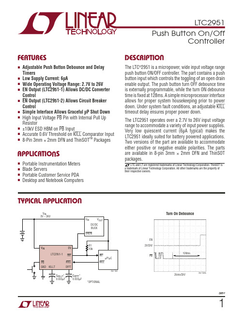
TOP VIEW
GND 1
8 INT
KILLT 2
7 EN/EN
9
PB 3
6 OFFT
VIN 4
5 KILL
DDBห้องสมุดไป่ตู้ PACKAGE 8-LEAD (3mm × 2mm) PLASTIC DFN
- 1、下载文档前请自行甄别文档内容的完整性,平台不提供额外的编辑、内容补充、找答案等附加服务。
- 2、"仅部分预览"的文档,不可在线预览部分如存在完整性等问题,可反馈申请退款(可完整预览的文档不适用该条件!)。
- 3、如文档侵犯您的权益,请联系客服反馈,我们会尽快为您处理(人工客服工作时间:9:00-18:30)。
FEATURESOUTPUTGNDINPUT12348765INPUTFEEDBACKV TAPERROROUTPUTSENSESHUTDOWNGNDLP2951...D (SOIC) PACKAGE(TOP VIEW)LP2950...LP (TO-226/TO-92 PACKAGE(BOTTOM VIEW)DESCRIPTION/ORDERING INFORMATIONWITH SHUTDOWNSLVS582D–APRIL2006–REVISED MARCH2007•Wide Input Range…up to30V•Stable With Low ESR(>12mΩ)Capacitors •Rated Output Current of100mA•Current-and Thermal-Limiting Features •Low Dropout…380mV(Typ)at100mA•LP2950Only(3-Pin Package)•Low Quiescent Current…75µA(Typ)–Fixed-Output Voltages of5V,3.3V,and3V•Tight Line Regulation…0.03%(Typ)•LP2951Only(8-Pin Package)•Tight Load Regulation…0.04%(Typ)–Fixed-or Adjustable-Output Voltages:•High V O Accuracy5V/ADJ,3.3V/ADJ,and3V/ADJ – 1.4%at25°C–Low-Voltage Error Signal on Falling Output –2%Over Temperature–Shutdown Capability•Can Be Used as a Regulator or Reference–Remote Sense Capability for OptimalOutput Regulation and AccuracyThe LP2950and LP2951devices are bipolar,low-dropout voltage regulators that can accommodate a wide input supply-voltage range of up to30V.The easy-to-use,3-pin LP2950is available in fixed-output voltages of5V, 3.3V,and3V.However,the8-pin LP2951is able to output either a fixed or adjustable output from the same device.By tying the OUTPUT and SENSE pins together,and the FEEDBACK and V TAP pins together,the LP2951outputs a fixed5V,3.3V,or3V(depending on the version).Alternatively,by leaving the SENSE and V TAP pins open and connecting FEEDBACK to an external resistor divider,the output can be set to any value between1.235V to30V.The8-pin LP2951also offers additional functionality that makes it particularly suitable for battery-powered applications.For example,a logic-compatible shutdown feature allows the regulator to be put in standby mode for power savings.In addition,there is a built-in supervisor reset function in which the ERROR output goes low when V OUT drops by6%of its nominal value for whatever reasons–due to a drop in V IN,current limiting,or thermal shutdown.The LP2950and LP2951are designed to minimize all error contributions to the output voltage.With a tight output tolerance(0.5%at25°C),a very low output voltage temperature coefficient(20ppm typical),extremely good line and load regulation(0.3%and0.4%typical),and remote sensing capability,the parts can be used as either low-power voltage references or100-mA regulators.Please be aware that an important notice concerning availability,standard warranty,and use in critical applications of TexasInstruments semiconductor products and disclaimers thereto appears at the end of this data sheet.PRODUCTION DATA information is current as of publication date.Copyright©2006–2007,Texas Instruments Incorporated Products conform to specifications per the terms of the TexasInstruments standard warranty.Production processing does notnecessarily include testing of all parameters.WITH SHUTDOWNSLVS582D–APRIL 2006–REVISED MARCH 2007ORDERING INFORMATION (1)V OUT ORDERABLE T APACKAGE (2)TOP-SIDE MARKING (NOM)PART NUMBER Bulk of 1000LP2950-30LP TO-226/TO-92–LPKY5030Reel of 2000LP2950-30LPR 3VTube of 75LP2951-30D SOIC –DKY5130Reel of 2500LP2951-30DR Bulk of 1000LP2950-33LP TO-226/TO-92–LPKY5033Reel of 2000LP2950-33LPR 3.3VTube of 75LP2951-33D –40°C to 125°CSOIC –DKY5133Reel of 2500LP2951-33DR Bulk of 1000LP2950-50LP PREVIEW TO-226/TO-92–LPReel of 2000LP2950-50LPR KY50505VTube of 75LP2951-50D SOIC –DKY5150Reel of 2500LP2951-50DR Tube of 75LP2951D ADJSOIC-DKY5150Reel of 2500LP2951DR(1)For the most current package and ordering information,see the Package Option Addendum at the end of this document,or see the TI website at .(2)Package drawings,standard packing quantities,thermal data,symbolization,and PCB design guidelines are available at /sc/package .2Submit Documentation FeedbackWITH SHUTDOWNSLVS582D–APRIL 2006–REVISED MARCH 2007LP2950FUNCTIONAL BLOCK DIAGRAMLP2951FUNCTIONAL BLOCK DIAGRAM3Submit Documentation FeedbackAbsolute Maximum Ratings (1)Recommended Operating ConditionsWITH SHUTDOWNSLVS582D–APRIL 2006–REVISED MARCH 2007over operating free-air temperature range (unless otherwise noted)MINMAX UNIT V IN Continuous input voltage range –0.330V V SHDN SHUTDOWN input voltage range–1.530V ERROR comparator output voltage range (2)–1.530V V FDBK FEEDBACK input voltage range (2)(3)–1.530V D package 97θJA Package thermal impedance (4)(5)°C/W LP package140T J Operating virtual junction temperature 150°C T stg Storage temperature range–65150°C(1)Stresses beyond those listed under "absolute maximum ratings"may cause permanent damage to the device.These are stress ratings only,and functional operation of the device at these or any other conditions beyond those indicated under "recommended operating conditions"is not implied.Exposure to absolute-maximum-rated conditions for extended periods may affect device reliability.(2)May exceed input supply voltage(3)If load is returned to a negative power supply,the output must be diode clamped to GND.(4)Maximum power dissipation is a function of T J (max),θJA ,and T A .The maximum allowable power dissipation at any allowable ambient temperature is P D =(T J (max)–T A )/θJA .Operating at the absolute maximum T J of 150°C can affect reliability.(5)The package thermal impedance is calculated in accordance with JESD 51-7.MINMAX UNIT V IN Supply input voltage(1)30V T J Operating virtual junction temperature–40125°C(1)Minimum V IN is the greater of:a.2V (25°C),2.3V (over temperature),orb.V OUT(MAX)+Dropout (Max)at rated I L4Submit Documentation FeedbackElectrical CharacteristicsWITH SHUTDOWN SLVS582D–APRIL2006–REVISED MARCH2007V IN =VOUT(nominal)+1V,IL=100µA,CL=1µF(5-V versions)or CL=2.2µF(3-V and3.3-V versions),8-pin version:FEEDBACK tied to VTAP ,OUTPUT tied to SENSE,VSHUTDOWN≤0.7VPARAMETER TEST CONDITIONS T J MIN TYP MAX UNIT3-V VERSION(LP295x-30)25°C 2.9703 3.030V OUT Output voltage I L=100µA V–40°C to125°C 2.9403 3.0603.3-V VERSION(LP295x-33)25°C 3.267 3.3 3.333V OUT Output voltage I L=100µA V–40°C to125°C 3.234 3.3 3.3665-V VERSION(LP295x-50)25°C 4.9505 5.050V OUT Output voltage I L=100µA V–40°C to125°C 4.9005 5.100ALL VOLTAGE OPTIONSOutput voltage temperatureI L=100µA–40°C to125°C20100ppm/°Ccoefficient(1)25°C0.030.2 Line regulation(2)V IN=[V OUT(NOM)+1V]to30V%/V–40°C to125°C0.425°C0.040.2 Load regulation(2)I L=100µA to100mA%–40°C to125°C0.325°C5080I L=100µA–40°C to125°C150V IN–V OUT Dropout voltage(3)mV25°C380450I L=100mA–40°C to125°C60025°C75120I L=100µAµA–40°C to125°C140I GND GND current25°C812I L=100mA mA–40°C to125°C1425°C110170V IN=V OUT(NOM)–0.5V,Dropout ground currentµAI L=100µA–40°C to125°C20025°C160200 Current limit V OUT=0V mA–40°C to125°C220 Thermal regulation(4)I L=100µA25°C0.050.2%/WC L=1µF(5V only)430C L=200µF160Output noise(RMS),25°CµVLP2951-50:C L=3.3µF,10Hz to100kHzC Bypass=0.01µF between pins1100and7(LP2951-xx)8-PIN VERSION ONLY ADJ25°C 1.218 1.235 1.252–40°C to125°C 1.212 1.257Reference voltage VV OUT=V REF to(V IN–1V),V IN=2.3V to30V,–40°C to125°C 1.200 1.272I L=100µA to100mAReference voltage25°C20ppm/°C temperature coefficient(1)(1)Output or reference voltage temperature coefficient is defined as the worst-case voltage change divided by the total temperature range.(2)Regulation is measured at constant junction temperature,using pulse testing with a low duty cycle.Changes in output voltage due toheating effects are covered under the specification for thermal regulation.(3)Dropout voltage is defined as the input-to-output differential at which the output voltage drops100mV,below the value measured at1-Vdifferential.The minimum input supply voltage of2V(2.3V over temperature)must be observed.(4)Thermal regulation is defined as the change in output voltage at a time(T)after a change in power dissipation is applied,excluding loador line regulation effects.Specifications are for a50-mA load pulse at V IN=30V,V OUT=5V(1.25-W pulse)for t=10ms.5Submit Documentation FeedbackWITH SHUTDOWNSLVS582D–APRIL 2006–REVISED MARCH 2007Electrical Characteristics (continued)V IN =V OUT (nominal)+1V,I L =100µA,C L =1µF (5-V versions)or C L =2.2µF (3-V and 3.3-V versions),8-pin version:FEEDBACK tied to V TAP ,OUTPUT tied to SENSE,V SHUTDOWN ≤0.7VPARAMETER TEST CONDITIONST J MINTYP MAX UNIT 25°C 2040FEEDBACK bias current nA –40°C to 125°C60FEEDBACK bias current 25°C0.1nA/°Ctemperature coefficientERROR COMPARATOR25°C 0.011Output leakage current V OUT =30VµA –40°C to 125°C225°C 150250V IN =V OUT(NOM)–0.5V,Output low voltage mV I OL =400µA–40°C to 125°C40025°C 4060Upper threshold voltage mV (ERROR output high)(5)–40°C to 125°C2525°C 7595Lower threshold voltage mV (ERROR output low)(5)–40°C to 125°C140Hysteresis (6)25°C15mVSHUTDOWN INPUTLow (regulator ON)0.7Input logic voltage–40°C to 125°CVHigh (regulator OFF)225°C 3050V TAP =2.4V–40°C to 125°C100SHUTDOWN input currentµA 25°C 450600V TAP =30V–40°C to 125°C750V SHUTDOWN ≥2V,25°C 310Regulator output current V IN ≤30V,V OUT =0,µA in shutdown–40°C to 125°C20FEEDBACK tied to V TAP(5)Comparator thresholds are expressed in terms of a voltage differential equal to the nominal reference voltage (measured atV IN –V OUT =1V)minus FEEDBACK terminal voltage.To express these thresholds in terms of output voltage change,multiply by the error amplifier gain =V OUT /V REF =(R1+R2)/R2.For example,at a programmed output voltage of 5V,the ERROR output is specified to go low when the output drops by 95mV ×5V/1.235V =384mV.Thresholds remain constant as a percentage of V OUT (as V OUT is varied),with the low-output warning occurring at 6%below nominal (typ)and 7.7%(max).(6)Comparator thresholds are expressed in terms of a voltage differential equal to the nominal reference voltage (measured atV IN –V OUT =1V)minus FEEDBACK terminal voltage.To express these thresholds in terms of output voltage change,multiply by the error amplifier gain =V OUT /V REF =(R1+R2)/R2.For example,at a programmed output voltage of 5V,the ERROR output is specified to go low when the output drops by 95mV ×5V/1.235V =384mV.Thresholds remain constant as a percentage of V OUT (as V OUT is varied),with the low-output warning occurring at 6%below nominal (typ)and 7.7%(max).6Submit Documentation FeedbackTYPICALCHARACTERISTICS0.010.11100.00010.0010.010.1I L –Load Current –AQ u i e s c e n t C u r r e n t –m A0102030405060708090100V IN –Input Voltage –VI n p u t C u r r e n t –µA020406080100120140160180200012345678910V IN –Input Voltage –VI n p u t C u r r e n t –µA010203040506070809010011012012345678910V IN –Input Voltage –VI n p u t C u r r e n t –m AWITH SHUTDOWNSLVS582D–APRIL 2006–REVISED MARCH 2007QUIESCENT CURRENTINPUT CURRENTvsvsLOAD CURRENTINPUT VOLTAGEINPUT CURRENTINPUT CURRENTvsvsINPUT VOLTAGEINPUT VOLTAGE7Submit Documentation Feedback4.9004.9254.9504.9755.0005.0255.0505.0755.100-40-25-105203550658095110125T A –Temperature –°C V O U T –O u t p u t V o l t a g e –V102030405060708090100110120V IN –Input Voltage –VQ u i e s c e n t C u r r e n t –µA12345678012345678V IN –Input Voltage –VQ u i e s c e n t C u r r e n t –µA0102030405060708090100110120012345678V IN –Input Voltage –VQ u i e s c e n t C u r r e n t –µAWITH SHUTDOWNSLVS582D–APRIL 2006–REVISED MARCH 2007TYPICAL CHARACTERISTICS (continued)OUTPUT VOLTAGEQUIESCENT CURRENTvsvsTEMPERATUREINPUT VOLTAGEQUIESCENT CURRENTQUIESCENT CURRENTvsvsINPUT VOLTAGEINPUT VOLTAGE8Submit Documentation Feedback50556065707580859095100-40-25-105203550658095110125T A –Temperature –°CQ u i e s c e n t C u r r e n t –µA55.566.577.588.599.510-40-25-105203550658095110125T A –Temperature –°CQ u i e s c e n t C u r r e n t –mA5075100125150175200225250-40-25-105203550658095110125T A –Temperature –°CS h o r t -C i r c u i t C u r r e n t –A50100150200250300350400450500-40-25-105203550658095110125T A –Temperature –°C(V I N –V O U T )–D r o p o u t V o l t a g e –m VWITH SHUTDOWNSLVS582D–APRIL 2006–REVISED MARCH 2007TYPICAL CHARACTERISTICS (continued)QUIESCENT CURRENTQUIESCENT CURRENTvsvsTEMPERATURETEMPERATURESHORT-CIRCUIT CURRENTDROPOUT VOLTAGEvsvsTEMPERATURETEMPERATURE9Submit Documentation Feedback1.61.651.71.751.81.851.91.952-40-25-105203550658095110125T A –Temperature –°CM i n i m u m O p e r a t i n g V o l t a g e –V501001502002503003504000.00010.0010.010.1I O –Output Current –A (V I N –V O U T )–D r o p o u t V o l t a g e –m V012345678012345678V IN –Input Voltage –VE R R O R O u t p u t –V-20-15-10-5051015202530-55-30-520457095120145T A –Temperature –°CF E E D B A C K B i a s C u r r e n t –n AWITH SHUTDOWNSLVS582D–APRIL 2006–REVISED MARCH 2007TYPICAL CHARACTERISTICS (continued)DROPOUT VOLTAGELP2951MINIMUM OPERATING VOLTAGEvsvsOUTPUT CURRENTTEMPERATURELP2951FEEDBACK BIAS CURRENTLP2951ERROR COMPARATOR OUTPUTvsvsTEMPERATUREINPUT VOLTAGE10Submit Documentation FeedbackInput Voltage2V/divOutput Voltage80 mV/div00.250.50.7511.251.51.75200.10.20.30.40.50.60.70.80.9V OL –Output Low Voltage –VI S I N K –S i n k C u r r e n t –m AOutput Load 100 mA/divOutput Voltage100 mV/divOutput Load 100 mA/divOutput Voltage100 mV/divLP2950,LP2951ADJUSTABLE MICROPOWER VOLTAGE REGULATORSWITH SHUTDOWNSLVS582D–APRIL 2006–REVISED MARCH 2007TYPICAL CHARACTERISTICS (continued)LP2951ERROR COMPARATOR SINK CURRENTLINE TRANSIENT RESPONSEvsvs OUTPUT LOW VOLTAGETIMELOAD TRANSIENT RESPONSELOAD TRANSIENT RESPONSEvs vs TIMETIME(V OUT =5V,C L =1µF)(V OUT =5V,C L =10µF)20304050607080901.E+011.E+021.E+031.E+041.E+051.E+06f –Frequency –HzP o w e r -S u p p l y R i p p l e R e j e c t i o n –d B101001k 10k 100k1M 0.010.11101001.E+011.E+02 1.E+03 1.E+04 1.E+05 1.E+06f –Frequency –HzO u t p u t I m p e d a n c e –Oh m 101001k 10k 100k 1M ΩLP2950,LP2951ADJUSTABLE MICROPOWER VOLTAGE REGULATORS WITH SHUTDOWNSLVS582D–APRIL 2006–REVISED MARCH 2007TYPICAL CHARACTERISTICS (continued)ENABLE TRANSIENT RESPONSEENABLE TRANSIENT RESPONSEvs vs TIMETIME(C L =1µF,I L =1mA)(C L =10µF,I L =1mA)OUTPUT IMPEDANCERIPPLE REJECTIONvsvsFREQUENCYFREQUENCY1020304050607080901001.E+01 1.E+02 1.E+03 1.E+04 1.E+05 1.E+06f –Frequency –HzP o w e r -S u p p l y R i p p l e R e j e c t i o n –d B101001k10k100k1M1020304050607080901001.E+011.E+02 1.E+03 1.E+04 1.E+05 1.E+06f –Frequency –HzP o w e r -S u pp l y R i p p l e R e j e c t i o n –d B101001k 10k 100k 1M 050100150200250300350400-40-25-105203550658095110125T A –Temperature –°CR P 2P 4–P i n 2t o P i n 4R e s i s t a n c e –k W1234561.E+01 1.E+02 1.E+03 1.E+04 1.E+05f –Frequency –HzO u t p u t N o i s e –µVµF µF 101001k10k100kLP2950,LP2951ADJUSTABLE MICROPOWER VOLTAGE REGULATORSWITH SHUTDOWNSLVS582D–APRIL 2006–REVISED MARCH 2007TYPICAL CHARACTERISTICS (continued)RIPPLE REJECTIONRIPPLE REJECTIONvsvsFREQUENCYFREQUENCYLP2951OUTPUT NOISELP2951DIVIDER RESISTANCEvsvsFREQUENCYTEMPERATURE0.80.911.11.21.31.41.51.61.7-40-25-105203550658095110125T A–Temperature–°CInputLogicVoltage(OFFtoON)–V0.80.911.11.21.31.41.51.61.7-40-25-105203550658095110125T A–Temperature–°CInputLogicVoltage(ONtoOFF)–V-2-11234560510********V IN–Input Voltage–VOutputVoltageChange–mVLP2950,LP2951ADJUSTABLE MICROPOWER VOLTAGE REGULATORSWITH SHUTDOWNSLVS582D–APRIL2006–REVISED MARCH2007TYPICAL CHARACTERISTICS(continued)SHUTDOWN THRESHOLD VOLTAGE(OFF TO ON)SHUTDOWN THRESHOLD VOLTAGE(ON TO OFF)vs vsTEMPERATURE TEMPERATURELINE REGULATIONvsINPUT VOLTAGEAPPLICATION INFORMATION Input Capacitor(C IN)Output Capacitor(C OUT)Capacitance ValueESR Range LP2950,LP2951ADJUSTABLE MICROPOWER VOLTAGE REGULATORSWITH SHUTDOWNSLVS582D–APRIL2006–REVISED MARCH2007A1-µF(tantalum,ceramic,or aluminum)electrolytic capacitor should be placed locally at the input of the LP2950or LP2951if there is,or will be,significant impedance between the ac filter capacitor and the input;for example,if a battery is used as the input or if the ac filter capacitor is located more than10in away.There are no ESR requirements for this capacitor,and the capacitance can be increased without limit.As with most PNP LDOs,stability conditions require the output capacitor to have a minimum capacitance and an ESR that falls within a certain range.For V OUT≥5V,a minimum of1µF is required.For lower V OUT,the regulator’s loop gain is running closer to unity gain and,thus,has lower phase margins.Consequently,a larger capacitance is needed for stability.For V OUT=3V or3.3V,a minimum of2.2µF is recommended.For worst case,V OUT=1.23V(using the ADJ version),a minimum of3.3µF is recommended.C OUT can be increased without limit and only improves the regulator stability and transient response.Regardless of its value,the output capacitor should have a resonant frequency less than500kHz.The minimum capacitance values given above are for maximum load current of100mA.If the maximum expected load current is less than100mA,then lower values of C OUT can be used.For instance,if I OUT<10 mA,then only0.33µF is required for C OUT.For I OUT<1mA,0.1µF is sufficient for stability requirements.Thus, for a worst-case condition of100-mA load and V OUT=V REF=1.235V(representing the highest load current and lowest loop gain),a minimum C OUT of3.3µF is recommended.For the LP2950,no load stability is inherent in the design—a desirable feature in CMOS circuits that are put in standby(such as RAM keep-alive applications).If the LP2951is used with external resistors to set the output voltage,a minimum load current of1µA is recommended through the resistor divider.The regulator control loop relies on the ESR of the output capacitor to provide a zero to add sufficient phase margin to ensure unconditional regulator stability;this requires the closed-loop gain to intersect the open-loop response in a region where the open-loop gain rolls off at20dB/decade.This ensures that the phase always is less than180°(phase margin greater than0°)at unity gain.Thus,a minimum-maximum range for the ESR must be observed.The upper limit of this ESR range is established by the fact that too high an ESR could result in the zero occurring too soon,causing the gain to roll off too slowly,which,in turn allows a third pole to appear before unity gain and introduce enough phase shift to cause instability.This typically limits the max ESR to approximately 5Ω.Conversely,the lower limit of the ESR is tied to the fact that too low an ESR shifts the zero too far out(past unity gain)and,thus,allows the gain to roll off at40dB/decade at unity gain,with a resulting phase shift of greater than180°.Typically,this limits the minimum ESR to approximately20mΩto30mΩ.For specific ESR requirements,see Typical Characteristics.Capacitor TypesC BYPASS :Noise and Stability Improvementf (CBYPASS)]200Hz ³C BYPASS +12p R1 200Hz (1)ERROR Function (LP2951Only)LP2950,LP2951ADJUSTABLE MICROPOWER VOLTAGE REGULATORS WITH SHUTDOWNSLVS582D–APRIL 2006–REVISED MARCH 2007APPLICATION INFORMATION (continued)Most tantalum or aluminum electrolytics are suitable for use at the input.Film-type capacitors also work,but at higher cost.When operating at low temperature,care should be taken with aluminum electrolytics,as their electrolytes often freeze at –30°C.For this reason,solid tantalum capacitors should be used at temperatures below –25°C.Ceramic capacitors can be used,but due to their low ESR (as low as 5m Ωto 10m Ω),they may not meet the minimum ESR requirement previously discussed.If a ceramic capacitor is used,a series resistor between 0.1Ωto 2Ωmust be added to meet the minimum ESR requirement.In addition,ceramic capacitors have one glaring disadvantage that must be taken into account —a poor temperature coefficient,where the capacitance can vary significantly with temperature.For instance,a large-value ceramic capacitor (≥2.2µF)can lose more than half of its capacitance as temperature rises from 25°C to 85°C.Thus,a 2.2-µF capacitor at 25°C drops well below the minimum C OUT required for stability as ambient temperature rises.For this reason,select an output capacitor that maintains the minimum 2.2-µF required for stability for the entire operating temperature range.In the LP2951,an external FEEDBACK pin directly connected to the error amplifier noninverting input can allow stray capacitance to cause instability by shunting the error amplifier feedback to GND,especially at high frequencies.This is worsened if high-value external resistors are used to set the output voltage,because a high resistance allows the stray capacitance to play a more significant role;i.e.,a larger RC time delay is introduced between the output of the error amplifier and its FEEDBACK input,leading to more phase shift and lower phase margin.A solution is to add a 100-pF bypass capacitor (C BYPASS )between OUTPUT and FEEDBACK;because C BYPASS is in parallel with R1,it lowers the impedance seen at FEEDBACK at high frequencies,in effect offsetting the effect of the parasitic capacitance by providing more feedback at higher frequencies.More feedback forces the error amplifier to work at a lower loop gain,so C OUT should be increased to a minimum of 3.3µF to improve the regulator’s phase margin.C BYPASS can be also used to reduce output noise in the LP2951.This bypass capacitor reduces the closed loop gain of the error amplifier at the high frequency,so noise no longer scales with the output voltage.This improvement is more noticeable with higher output voltages,because loop gain reduction is greatest.A suitable C BYPASS is calculated as shown in Equation 1:On the 3-pin LP2950,noise reduction can be achieved by increasing the output capacitor,which causes theregulator bandwidth to be reduced,therefore,eliminating high-frequency noise.However,this method is relatively inefficient,as increasing C OUT from 1µF to 220µF only reduces the regulator’s output noise from 430µV to 160µV (over a 100-kHz bandwidth).The LP2951has a low-voltage detection comparator that outputs a logic low when the output voltage drops by ≈6%from its nominal value,and outputs a logic high when V OUT has reached ≈95%of its nominal value.This 95%of nominal figure is obtained by dividing the built-in offset of ≈60mV by the 1.235-V bandgap reference,and remains independent of the programmed output voltage.For example,the trip-point threshold (ERROR output goes high)typically is 4.75V for a 5-V output and 11.4V for a 12-V output.Typically,there is a hysteresis of 15mV between the thresholds for high and low ERROR output.A timing diagram is shown in Figure 1for ERROR vs V OUT (5V),as V IN is ramped up and down.ERROR becomes valid (low)when V IN ≈1.3V.When V IN ≈5V,V OUT =4.75V,causing ERROR to go high.Because the dropout voltage is load dependent,the output trip-point threshold is reached at different values of V IN ,depending on the load current.For instance,at higher load current,ERROR goes high at a slightly higher value of V IN ,and vice versa for lower load current.The output-voltage trip point remains at ≈4.75V,regardless of the load.Note that when V IN ≤1.3V,the ERROR comparator output is turned off and pulled high to its pullup voltage.If V OUT is used as the pullup voltage,rather than an external 5-V source,ERROR typically is ≈1.2V.In this condition,an equal resistor divider (10k Ωis suitable)can be tied to ERROR to divide down the voltage to a valid logic low during any fault condition,while still enabling a logic high during normal operation.5 V1.3 VInput VoltageOutput VoltageERROR4.75 VProgramming Output Voltage (LP2951Only)V OUT +V REF ǒ1)R1R2Ǔ*I FB R 1(2)LP2950,LP2951ADJUSTABLE MICROPOWER VOLTAGE REGULATORSWITH SHUTDOWNSLVS582D–APRIL 2006–REVISED MARCH 2007APPLICATION INFORMATION (continued)Figure 1.ERROR Output TimingBecause the ERROR comparator has an open-collector output,an external pullup resistor is required to pull the output up to V OUT or another supply voltage (up to 30V).The output of the comparator is rated to sink up to 400µA.A suitable range of values for the pullup resistor is from 100k Ωto 1M Ω.If ERROR is not used,it can be left open.A unique feature of the LP2951is its ability to output either a fixed voltage or an adjustable voltage,depending on the external pin connections.To output the internally programmed fixed voltage,tie the SENSE pin to the OUTPUT pin and the FEEDBACK pin to the V TAP pin.Alternatively,a user-programmable voltage ranging from the internal 1.235-V reference to a 30-V max can be set by using an external resistor divider pair.The resistor divider is tied to V OUT ,and the divided-down voltage is tied directly to FEEDBACK for comparison against the internal 1.235-V reference.To satisfy the steady-state condition in which its two inputs are equal,the error amplifier drives the output to equal Equation 2:Where:V REF =1.235V applied across R2I FB =FEEDBACK bias current,typically 20nAA minimum regulator output current of 1µA must be maintained.Thus,in an application where a no-load condition is expected (for example,CMOS circuits in standby),this 1-µA minimum current must be provided by the resistor pair,effectively imposing a maximum value of R2=1.2M Ω(1.235V/1.2M Ω≈1µA).I FB =20nA introduces an error of ≈0.02%in V OUT .This can be offset by trimming R1.Alternatively,increasing the divider current makes I FB less significant,thus,reducing its error contribution.For instance,using R2=100k Ωreduces the error contribution of I FB to 0.17%by increasing the divider current to ≈12µA.This increase in the divider current still is small compared to the 600-µA typical quiescent current of the LP2951under no load.。