TM2302 (3A车充芯片)
国轩高科给大众供应的电芯参数

国轩高科给大众供应的电芯参数一、简介国轩高科是一家在新能源领域具有领先地位的企业,专注于锂离子电池技术的研发和生产。
作为国内领先的电池制造商之一,国轩高科向大众汽车公司提供优质的电芯产品,为大众汽车的电动车型提供强大的动力支持。
本文将详细介绍国轩高科所供应的电芯参数。
二、国轩高科电芯参数2.1 型号国轩高科为大众汽车供应的电芯主要包括以下几个型号:1.NCM523:这是一种镍锰钴酸锂电池,其比容量高,性能稳定;2.NCM622:这是一种镍钴锰酸锂电池,具有较高的能量密度和更长的寿命;3.NCM811:这是一种镍钴锰酸锂电池,具有非常高的能量密度和出色的动力性能;2.2 容量国轩高科为大众汽车供应的电芯容量可以根据客户需求进行定制,包括2000mAh、2500mAh、3000mAh等不同容量等级。
这样的定制化服务可以满足大众汽车不同车型和不同行驶里程的需求。
2.3 电压国轩高科的电芯具有稳定的工作电压范围,通常为3.6V-3.7V。
这一电压范围非常适合大众汽车的电动车辆,可以提供稳定的动力输出。
2.4 重量国轩高科的电芯重量相对较轻,是传统燃油车型的1/3左右。
这不仅有助于提高电动车的整体能效,还可以减少车辆的自重,提高行驶里程和操控性能。
2.5 寿命国轩高科的电芯寿命较长,可以达到3000-5000次循环。
这意味着一块电芯可以使用多年,大大延长了电动车的使用寿命,减少了用户的更换成本。
2.6 充电速度国轩高科的电芯支持快速充电,具有较高的充电速度。
根据客户需求,电芯可以在较短的时间内实现0%-80%的充电,大大缩短了充电时间,提高了用户的使用便利性。
三、总结国轩高科作为一家在新能源领域具有领先地位的企业,为大众汽车提供了优质的电芯产品。
这些电芯具有多种型号可供选择,包括NCM523、NCM622和NCM811等。
它们具有稳定的工作电压范围、较长的使用寿命、较高的能量密度和快速充电等优点。
国轩高科的电芯参数符合大众汽车对动力性能和可靠性的要求,为大众汽车的电动车型提供了可靠的动力支持。
2023年全国大学生电子设计竞赛C题

目录摘要 (3)1.设计任务及规定 (4)1.1设计任务 (4)1.2设计规定 (4)2.系统方案 (5)2.1控制模块旳论证与选择 (5)2.2电源模块旳论证与选择 (5)2.3小车车体旳论证与选择 (6)2.4电机模块旳论证与选择 (6)2.5电机驱动模块旳论证与选择 (6)2.6寻迹模块旳论证与选择 (7)2.7避障模块旳论证与选择 (7)2.8显示模块旳论证与选择 (7)2.9按键模块旳论证与选择 (8)2.10通信模块旳论证与选择 (8)2.11方案选定 (9)3.系统旳理论分析与计算 (10)3.1系统旳信号检测与控制 (10)3.1.1 系统旳信号检测 (10)3.1.2 系统旳信号控制 (10)3.2 两车之间旳通信措施 (11)3.3 节能 (11)4.电路与程序设计 (12)4.1电路旳设计 (12)4.1.1 系统总体框图 (12)4.1.2 控制器旳电路设计 (13)4.1.3 稳压电源旳电路设计 (13)4.1.4 电机驱动电路旳设计 (14)4.2程序旳设计 (15)4.2.1 程序功能描述与设计 (15)4.2.2 程序流程图 (16)5.测试措施与测试成果 (19)5.1测试方案 (19)5.2测试条件与仪器 (19)5.3测试成果及分析 (19)5.3.1 测试数据 (19)5.3.2测试分析与结论 (19)参照文献 (17)附录1 (18)附录2 (19)附录3 (20)智能小车旳设计摘要: 本作品以低功耗旳ATmega16单片机为控制关键;MP2307稳压电路供电;使用光电传感器寻线和避障;LN298N驱动电机;以光电传感器来实现甲乙两车之间旳通信;结合了PWM调速等技术, 设计了一组智能小车。
该小车旳车体由控制、电源、按键、小车硬件、电机、电机驱动、寻迹、避障、显示和光电传感通信等十个模块构成, 可用于无人驾驶、自动探测等人工智能领域。
关键字: ATmega16.MP2307、光电、LN298N1.设计任务及规定1.1设计任务甲车车头紧靠起点标志线,乙车车尾紧靠边界,甲、乙两辆小车同步起动, 先后通过起点标志线, 在行车道同向而行, 实现两车交替超车领跑功能。
TM1826
PALED104 PALED103 PALED105 PALED102
PALED106 PALED101 PAU108 COC5 COR20COR19 PAU107 PAU106 PAC502 PAR201 PAR1902 PAU105 PAC501 PAR202 PAR1901
COQ4 COR4 COQ2 PAQ403 CPAORR4021 PAR402PAQ203 PAQ402 PAQ401 PAR201 PAR202PAQ202COPAQ20L1 ED24
(TOP VIEW)
16 DIN 15 OUT B1 14 OUT G1 13 OUT R1 12 OUT B2 11 OUT G2 10 OUT R2 9 GND
深圳市天微电子有限公司 原厂原装IC 覃先生 :13751069293 15377886521 QQ: 670505985 输出及输入等效电路
702UAP 602UAP 502UAP 402UAP 802UAP 902UAP 102UAP 102UAP
COLED12 PALED1201 PALED1206 PALED1202 PALED1205 COR28 PALED1203 PALED1204
PAR2801 PAR2802
COLED11 PALED1101 PALED1106
VDD
VDD
OUTn
DIN
DO
GND
GND
GND
V1.1
2
管脚功能
十二通道 LED 恒流驱动 TM1826
名称
DIN DO OUTR1 OUTG1 OUTB1 OUTR2 OUTG2 OUTB2 OUTR3 OUTG3 OUTB3 OUTR4 OUTG4 OUTB4 VDD GND
《基于ISO26262的汽车电子功能安全:方法与应用》笔记
《基于ISO26262的汽车电子功能安全:方法与应用》读书札记目录一、内容描述 (2)1.1 书籍简介 (3)1.2 ISO26262标准概述 (4)二、汽车电子功能安全基础 (5)2.1 功能安全概念 (6)2.2 ISO26262标准体系 (8)2.3 功能安全等级 (9)三、ISO26262在汽车电子中的应用 (11)3.1 驱动电机控制系统 (12)3.2 电池管理系统 (14)3.3 传感器与执行器 (15)3.4 车载通信系统 (17)四、功能安全方法与技术 (18)4.1 安全需求分析 (19)4.2 安全完整性等级 (21)4.3 故障模式与影响分析 (22)4.4 控制器设计与测试 (24)4.5 人机界面设计 (26)五、案例分析 (27)5.1 案例一 (29)5.2 案例二 (29)六、实践与建议 (30)6.1 企业实施功能安全的步骤 (32)6.2 政策建议与行业标准 (33)七、总结与展望 (35)7.1 本书总结 (36)7.2 未来发展趋势 (37)一、内容描述《基于ISO2的汽车电子功能安全:方法与应用》是一本关于汽车电子系统功能安全的专业书籍,作者通过对国际标准化组织(ISO)2标准的研究和实践,详细介绍了汽车电子功能安全的基本概念、原则、方法和技术。
本书旨在帮助读者深入了解汽车电子功能安全的重要性,掌握相关的理论知识,并能够将其应用于实际的汽车电子系统中。
本书共分为五个部分:第一部分为引言,介绍了汽车电子功能安全的背景、意义和发展趋势;第二部分为ISO2标准概述,详细解读了ISO2标准的体系结构、架构和要求;第三部分为基础知识和方法,包括汽车电子系统的安全性分析、故障模式与影响分析(FMEA)、耐久性测试等方面的内容;第四部分为实际应用案例,通过分析典型的汽车电子系统实例,展示了如何将ISO2标准应用于实际项目中;第五部分为结论和展望,总结了本书的主要内容,并对未来汽车电子功能安全的发展进行了展望。
芯片推力测试标准
芯片推力测试标准
芯片推力测试是对火箭发动机或其他推进系统使用的燃料、推进剂进行性能测试的过程。
以下是针对芯片推力测试的一些常用标准:
1. ASTM E1445-16a标准:这个标准是关于使用液体或可压缩气体驱动装置进行燃料喷雾测试的标准,可以用于推力测试的燃料喷雾性能测试。
2. NASA-STD-5017标准:这个标准是关于液体燃料推进系统验证的要求和测试过程的标准,提供了方便和一致的测试程序来评估液体燃料推进系统的性能。
3. MIL-STD-1561C标准:这个标准是关于燃料喷雾性能测试要求和测试方法的标准,适用于火箭发动机和其他推进系统的燃料喷雾性能测试。
4. ASTM E2786-11标准:这个标准是关于测试当量比脉冲和比冲性能的推进系统的标准,通常适用于火箭发动机和其他推进系统。
5. ISO 22734-1标准:这个标准是关于推力测试和测量要求的标准,提供了用于推力测试的一般性能要求和测量精度要求。
AM2302中文资料

数字温湿度传感器AM2302数字温湿度传感器AM2302小体积AM2302►相对湿度和温度测量►全部校准,数字输出►卓越的长期稳定性►无需额外部件►超长的信号传输距离►超低能耗►4 引脚安装►完全互换AM2302产品概述AM2302数字温湿度传感器是一款含有已校准数字信号输出的温湿度复合传感器。
它应用专用的数字模块采集技术和温湿度传感技术,确保产品具有极高的可靠性与卓越的长期稳定性。
传感器包括一个电容式感湿元件和一个NTC测温元件,并与一个高性能8位单片机相连接。
因此该产品具有品质卓越、超快响应、抗干扰能力强、性价比极高等优点。
每个AM2302传感器都在极为精确的湿度校验室中进行校准。
校准系数以程序的形式储存在OTP内存中,传感器内部在检测信号的处理过程中要调用这些校准系数。
单线制串行接口,使系统集成变得简易快捷。
超小的体积、极低的功耗,信号传输距离可达20米以上,使其成为各类应用甚至最为苛刻的应用场合的最佳选则。
产品为 4 针单排引脚封装。
连接方便,特殊封装形式可根据用户需求而提供。
应用领域►暖通空调►测试及检测设备►汽车►数据记录器►消费品►自动控制►气象站►家电►湿度调节器►医疗3、接口说明建议连接线长度短于20米时用5K上拉电阻,大于20米时根据实际情况使用合适的上拉电阻AM2302的接线图如下图所示。
3、电源引脚AM2302的供电电压为3.3-6V。
传感器上电后,要等待1s 以越过不稳定状态在此期间无需发送任何指令。
电源引脚(VDD,GND)之间可增加一个100nF 的电容,用以去耦滤波。
4、单总线接口DATA 用于微处理器与AM2302之间的通讯和同步,采用单总线数据格式,一次通讯时间5ms左右,具体格式在下面说明,当前数据传输为40bit,高位先出。
数据格式: 40bit数据=16bit湿度数据+16bit温度数据+8bit校验和例子:接收40bit数据如下:0000 0010 1000 1100 0000 0001 0101 1111 1110 1110湿度数据温度数据校验和湿度高8位+湿度低8位+温度高8位+温度低8位=的末8位=校验和例如:0000 0010+1000 1100+0000 0001+0101 1111=1110 1110湿度=65.2%RH 温度=35.1℃当温度低于0℃时温度数据的最高位置1。
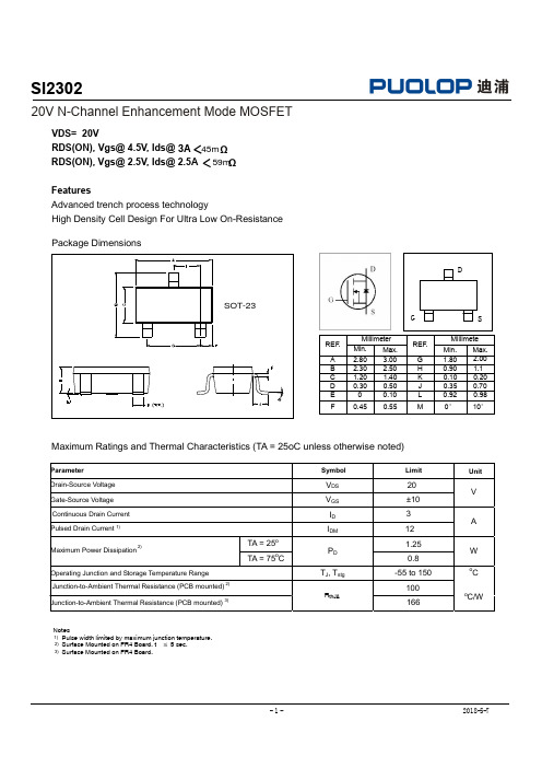
si2302中文资料_数据手册_参数
Unit
V
A
W oC oC/W
- 1-
2018-5-7
SI2302
ELECTRICAL CHARACTERISTICS
Parameter
Symbol
Test Condition
Static
Drain-Source Breakdown Voltage Drain-Source On-State Resistance 1)
Vdd
Rl
Vin
D
Vout
Vgs
Rgen
G
S
td(on)
VOUT
VIN
10%
ton
toff
tr
td(off)
tf
90%
INVERTED
10%
90% 10%
90%
50%
50%
PULSE WIDTH
Figure 1:Switching Test Circuit
Figure 2:Switching Waveforms
SOT-23
D
G
S
REF.
A B C D E
F
Millimeter
Min. Max.
2.80 3.00
2.30 2.50
1.20 1.40
0.30 0.50
0
0.10
0.45 0.55
REF.
G H K J L
M
Millimeter
Min. Max. 1.80 2.00 0.90 1.1 0.10 0.20 0.35 0.70 0.92 0.98
TA = 25o TA = 75oC
Symbol
VDS VGS ID IDM
第三代半导体驱动芯片的测试验证项目
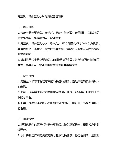
第三代半导体驱动芯片的测试验证项目一、项目背景1. 传统半导体驱动芯片在功耗、稳定性等方面存在局限性,难以满足未来高性能、高效能的电子设备需求。
2. 第三代半导体驱动芯片以碳化硅(SiC)和氮化镓(GaN)为代表,具有功耗小、速度快、稳定性高等优点,被视为未来半导体技术发展的重要方向。
3. 针对第三代半导体驱动芯片的测试验证项目,旨在验证其性能和可靠性,为其在电子设备中的应用提供可靠数据支持。
二、项目目标1. 对第三代半导体驱动芯片的功耗进行测试,验证其在高负载情况下的表现。
2. 对第三代半导体驱动芯片的稳定性进行测试,验证其在长时间工作下的可靠性。
3. 对第三代半导体驱动芯片的速度进行测试,验证其在高频率操作下的性能。
三、测试方案1. 选取代表性的第三代半导体驱动芯片作为测试样本,搭建相应的测试评台。
2. 设计并制定详细的测试方案,包括功耗测试、稳定性测试、速度测试等内容。
3. 针对每个测试项,明确测试指标和测试条件,确保测试结果的客观性和可比性。
4. 使用专业的测试设备和仪器,进行全面、系统的测试。
四、测试过程1. 在功耗测试中,通过在不同工作状态下测量功耗,分析芯片在不同负载下的功耗曲线和功耗特性。
2. 在稳定性测试中,对芯片进行长时间工作,观察其在恶劣环境下的稳定性表现,如温度变化、电压波动等情况。
3. 在速度测试中,通过在不同频率下进行操作,测量其响应速度和运行效率,分析其在高频率下的性能表现。
五、测试结果1. 通过测试,获得了第三代半导体驱动芯片在功耗、稳定性、速度等方面的详细测试数据。
2. 结果显示,该芯片在高负载下的功耗控制能力良好,稳定性在恶劣环境下表现出色,高频率下的运行效率也十分高。
3. 测试结果表明,第三代半导体驱动芯片具有优秀的性能和可靠性,适合应用于未来的高性能、高效能电子设备中。
六、项目意义1. 该测试验证项目为第三代半导体驱动芯片的性能和可靠性提供了客观、权威的数据支持,为其在电子设备中的应用提供了重要参考。
- 1、下载文档前请自行甄别文档内容的完整性,平台不提供额外的编辑、内容补充、找答案等附加服务。
- 2、"仅部分预览"的文档,不可在线预览部分如存在完整性等问题,可反馈申请退款(可完整预览的文档不适用该条件!)。
- 3、如文档侵犯您的权益,请联系客服反馈,我们会尽快为您处理(人工客服工作时间:9:00-18:30)。
DESCRIPTIONThe is a monolithic step-down switch mode converter with a built in internal power MOSFET. It achieves 2A continuous output cur-rent over a wide input supply range with excel-lent load and line regulation.The requires a minimum number ofreadily available standard external components. Current mode operation provides fast transient response and eases loop stabilization. shutdown mode the regulator draws 25µA of supply current.FEATURES●2A Output Current● 0.22Ω Internal Power MOSFET Switch ● Stable with Low ESR Output CeramicCapacitors ● Up to 95% Efficiency ● 25µA Shutdown Mode ●● Thermal Shutdown ● Cycle-by-Cycle Over Current Protection ● Wide 4.75 to 32V Operating InputRange ● Output Adjustable from 1.22V to 21VPACKAGE REFERENCEPart number Package Temperature–40°C to +125°CSOIC-8EL TM2302TM2302TM2302TM2302Fixed 420KHz Frequency Fault condition protection includes cycle-by-cycle current limiting and thermal shutdown. InMar.2009 Rev.1.1APPLICATIONS• Automotive Power Adapters• PDA and Cellular Phone Battery Chargers • Distributed Power Systems • Automotive Aftermarket Electronics2A 32V Step - DownABSOLUTE MAXIMUM RATINGS (1)Supply Voltage (V IN ) ........................................... 35V Switch Voltage (V SW ) .............................. –1V to V IN + 1V Bootstrap Voltage (V BS ) …............ Vsw-0.3V to V SW + 6V Enable/UVLO Voltage (V EN ) .................... –0.3V to +6VComp Voltage (V COMP )............................. –0.3V to +6V Feedback Voltage (V FB ) .......................... –0.3V to +6V Junction Temperature ................................. +150°C Lead Temperature ........................................ +260°C Storage Temperature ...................... –65°C to + 150°CRecommended Operating Conditions (2)Input Voltage (V IN ) ....................... 4.75V to 32VOperating Temperature ................. –40°C to + 125°CThermal Resistance (3) θJA θJCSOIC8EL .................................... 105 .. 50... °C/WNotes:1) Exceeding these ratings may damage the device. 2) The device is not guaranteed to function outside of its operating conditions.3) Measured on approximately 1” square of 1 oz copper.ELECTRICAL CHARACTERISTICSV IN = 12V, V EN = 5V,T A = +25°C, unless otherwise noted.ParameterCondition Min Typ Max Units Feedback Voltage4.75V ≤V IN ≤32V1.1841.230 1.258V Upper Switch-On Resistance 0.22 ΩLower Switch-On Resistance10ΩUpper Switch Leakage V EN = 0V, V SW = 0V10µA Current Limit2.5A Oscillator Frequency380420500KHz Short Circuit Frequency V FB = 0V 42 KHz Maximum Duty Cycle V FB = 1 .0V 90%Minimum Duty CycleV FB = 1 .5V0 %EN Shutdown Threshold Voltage I CC > 100µA 2.0 2.5 V EN UVLO Threshold Rising V EN Rising2.02.53.0V EN UVLO Threshold Hysteresis200mV Enable Pull-Up Current V EN = 0V 2µA Supply Current (Shutdown) V EN ≤0.4V 2550 µA Supply Current (Quiescent) V EN ≥2.6V, V FB = 1 .4V 1.0 1.5mAThermal Shutdown160°CTM23022A 32V Step - DownMar.2009 Rev.1.1PIN FUNCTIONSPin # Name Description1BSHigh-Side Gate Drive Boost Input. BS supplies the drive for the high-side N-channel MOSFET switch. Connect a 10nF or greater capacitor from SW to BS to power the switch.2 INPower Input. IN supplies the power to the IC, as well as the step-down converter switch. Drive In with a 4.75 to 35V power source. Bypass IN to GND with a suitably large capaci-tor to eliminate noise on the input to the IC. See Input Capacitor.Power Switching Output. SW is the switching node that supplies power to the output. Connect the output LC filter from SW to the output load. Note that a capacitor is required from SW to BS to power the high-side switch.5 GND Ground.Feedback Input. FB senses the output voltage to regulate that voltage. Drive FB with aresistive voltage divider from the output voltage. The feedback threshold is 1 .230V. See Setting the Output Voltage. Compensation Node. (optional)Enable Input. EN is a digital input that turns the regulator on or off. Drive EN high to turnon the regulator, low to turn it off. For automatic startup, leave EN unconnected.TM23023.4SW6FB7NC 8EN2A 32V Step - DownAPPLICATION INFORMATION COMPONENT SELECTIONSetting the Output VoltageThe output voltage is set using a resistive volt-age divider from the output voltage to FB (see Typical Application circuit on page 1). The volt-age divider divides the output voltage down bythe ratio:Where V FB is the feedback voltage and V OUT is the output voltage.Thus the output voltage is:R2 can be as high as 100kQ, but a typical value is 10k Ω. Using that value, R1 is determined by:For example, for a 3.3V output voltage, R2 is 10k Ω, and R1 is 16.9k Ω.InductorThe inductor is required to supply constant cur-rent to the output load while being driven by the switched input voltage. A larger value inductor results in less ripple current that results in lower output ripple voltage. However, the larger value inductor has a larger physical size, higher series resistance and/or lower saturation current. Choose an inductor that does not saturate under the worst-case load conditions. A good rule for determining the inductance is to allow the peak-to-peak ripple current in the inductor to be ap-proximately 30% of the maximum load current. Also, make sure that the peak inductor current (the load current plus half the peak-to-peak in-ductor ripple current) is below the 2.4A minimum current limit.The inductance value can be calculated by theequation:Where V IN is the input voltage, f is the switching frequency, and Äl is the peak-to-peak inductor ripple current.Table 1 lists a number of suitable inductors from vari-ous manufacturers. Table 1—Inductor Selection Guide Vendor/ Model Core Type Core Ma- terial Package Dimensions (mm)W L HSumidaCR75 Open Ferrite 7.0 7.8 5.5CDH74 Open Ferrite 7.3 8.0 5.2CDRH5D28 Shielded Ferrite 5.5 5.7 5.5CDRH5D28 Shielded Ferrite 5.5 5.7 5.5CDRH6D28 Shielded Ferrite 6.7 6.7 3.0CDRH104R Shielded Ferrite 10.1 10.0 3.0TokoD53LC Type A Shielded Ferrite 5.0 5.0 3.0D75C Shielded Ferrite 7.6 7.6 5.1D104C Shielded Ferrite 10.0 10.0 4.3D10FL Open Ferrite 9.7 1.5 4.0CoilcraftDO3308 Open Ferrite 9.4 13.03.0D03316 Open Ferrite 9.4 13.05.1Input CapacitorThe input current to the step-down converter is dis-continuous, and therefore an input capacitor C1 is required to supply the AC current to the step-down converter while maintaining the DC input voltage. A low ESR capacitor is required to keep the noise at the IC to a minimum. Ceramic capacitors are preferred, but tantalum or low-ESR electrolytic capacitors may also suffice.The input capacitor value should be greater than 10uF. The capacitor can be electrolytic, tantalum or ceramic. However, since it absorbs the input switch-ing current it requires an adequate ripple current rat-ing. Its RMS current rating should be greater than ap-proximately 1/2 of the DC load current.For insuring stable operation, C2 should be placed as close to the IC as possible. Alternately a smaller high quality ceramic 0.1 uF capacitor may be placed closer to the IC and a larger capacitor placed further away. If using this technique, it is recommended that the lar-ger capacitor be a tantalum or electrolytic type. All ceramic capacitors should be placed close to theTM2302.TM23022A 32V Step - DownChoose a rectifier the maximum reverse voltage rat-ing of which is greater than the maximum input volt-age, and has a current rating greater than the maxi-mum load current. CompensationThe system stability is controlled through the COMP pin. COMP is the output of the internal transconduc-tance error amplifier. A series capacitor-resistor combination sets a pole-zero combination to control the characteristics of the control system.The DC loop gain is:Where A VEA is the transconductance error amplifier voltage gain (400V/V), Gcs is the current sense gain (roughly the output current divided by the voltage at COMP) equal to 1.95 A/V and R LOAD is the load resis-tance (V OUT / I OU T where I 0UT is the output load cur-rent). The system has two poles of importance, one is due to the compensation capacitor (C3), and the other is due to the output capacitor (C2). These are:Where P1 is the first pole and G EA is the error ampli-fier transconductance (770uA/V). The other pole is: The system has one zero of importance, due to thecompensation capacitor (C3) and the compensation resistor (R3). The zero is:If a large value capacitor (C2) with relatively high equivalent-series-resistance (ESR) is used, the zero due to the capacitance and ESR of the output capaci-tor can be compensated by a third pole set by R3 and C6:The system crossover frequency (the frequency where the loop gain drops to 1 or O dB) is important. A good rule of thumb is to set the crossover fre-quency to approximately 1/10 of the switching fre-quency. In this case, the switching frequency is 420KHz. Therefore, use a crossover frequency (fc) of 40KHz. Lower crossover frequencies result in slower response and worse transient load recovery. Higher crossover frequencies can result in instability.Output CapacitorThe output capacitor is required to maintain the DC output voltage. Low ESR capacitors are preferred to keep the output voltage ripple low. The characteristics of the output capacitor also affect the stability of the regulation control sys-tem. Ceramic, tantalum or low ESR electrolytic capacitors are recommended. In the case of ceramic capacitors, the impedance at the switching frequency is dominated by the capaci-tance and so the output voltage ripple is mostly independent of the ESR. The output voltage ripple is estimated to be:In the case of tantalum or low-ESR electrolytic capacitors, the ESR dominates the impedance at the switching frequency, and so the output ripple is calculated as:V RIPPLE ؆ ∆I X R ESROutput Rectifier DiodeThe output rectifier diode supplies the current to the inductor when the high-side switch is off. Toreduce losses due to the diode forward voltage and recovery times, use a Schottky rectifier.Table 2 provides the Schottky rectifier partnumbers based on the maximum input voltageand current rating. TM23022A 32V Step - DownPACKAGE INFORMATIONTM2302 2A 32V Step - Down。