Interfacial characterization of resistance spot welded joint of steel and aluminum alloy
现代材料分析方法(英文)
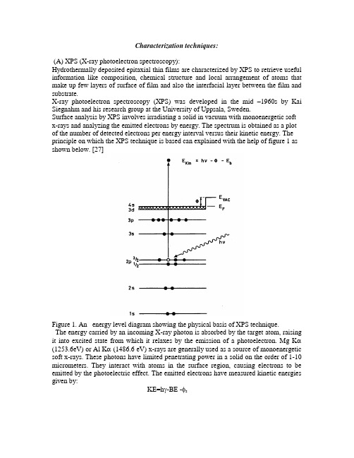
Characterization techniques:(A) XPS (X-ray photoelectron spectroscopy):Hydrothermally deposited epitaxial thin films are characterized by XPS to retrieve useful information like composition, chemical structure and local arrangement of atoms that make up few layers of surface of film and also the interfacial layer between the film and substrate.X-ray photoelectron spectroscopy (XPS) was developed in the mid –1960s by Kai Siegnahm and his research group at the University of Uppsala, Sweden.Surface analysis by XPS involves irradiating a solid in vacuum with monoenergetic soft x-rays and analyzing the emitted electrons by energy. The spectrum is obtained as a plot of the number of detected electrons per energy interval versus their kinetic energy. The principle on which the XPS technique is based can explained with the help of figure 1 as shown below. [27]Figure 1. An energy level diagram showing the physical basis of XPS technique.The energy carried by an incoming X-ray photon is absorbed by the target atom, raising it into excited state from which it relaxes by the emission of a photoelectron. Mg Kα(1253.6eV) or Al Kα (1486.6 eV) x-rays are generally used as a source of monoenergetic soft x-rays. These photons have limited penetrating power in a solid on the order of 1-10 micrometers. They interact with atoms in the surface region, causing electrons to be emitted by the photoelectric effect. The emitted electrons have measured kinetic energies given by:KE=hγ-BE -φsWhere hγ is the energy of the photon, BE is the binding energy of the atomic orbital from which the electron originates and φs is the spectrometer work function. The binding energy may be regarded as the energy difference between the initial and final states after the photoelectron has left the atom. Because there are a variety of possible final states of the ions from each type of atom, there is corresponding variety of kinetic energies of the emitted electrons. Photoelectrons are emitted from all energy levels of the target atom and hence the electron energy spectrum is characteristic of the emitting atom type and may be thought as its XPS fingerprint. Each element has unique spectrum .The spectrum from a mixture of elements is approximately the sum of peaks of the individual constituents. Because the mean free path of electrons in the solids is very small, the detected electrons originate from only the top few atomic layers making XPS a unique surface sensitive technique for chemical analysis. Quantitative data can be obtained from peak heights or peak areas and identification of chemical states often can be made from exact measurement of peak positions and separations as well from certain spectral features.The line lengths indicate the relative probabilities of the various ionization processes. The p,d and f levels split upon ionization leading to vacancies in the p1/2,p3/2,d3/2,d5/2,f5/2 and f7/2.The spin orbit splitting ratio is 1:2 for p levels ,2:3 for d levels and 3:4 for f levels .Because each element has a unique set of binding energies, XPS can be used to identify and determine the concentration of the elements in the surface. Variations in the elemental binding energies (the chemical shifts) arise from the differences in the chemical potential and polarizibilty of compounds. These chemical shifts can be analyzed to identify the chemical state of the materials being analyzed.The electrons leaving sample are detected by an electron spectrometer according to their kinetic energy. The analyzer is usually operated as an energy window, referred to as pass energy. To maintain a constant energy resolution, the pass energy is fixed. Incoming electrons are adjusted the pass energy before entering the energy analyzer. Scanning for different energies is accomplished by applying a variable electrostatic field before the analyzer. This retardation voltage may be varied from zero upto and beyond the photon energy. Electrons are detected as discrete events, and the number of electrons for the given detection time. And energy is stored and displayed.In general, the interpretation of the XPS spectrum is most readily accomplished first by identifying the lines that almost always present (specifically those of C and O), then by identifying major lines and associated weaker lines.(B) Auger electron spectroscopy:Auger electron spectroscopy is a very useful technique in elemental characterization of thin films. In the current project this technique has been utilized not only for elemental compositional analysis but also for understanding nucleation and growth mechanism. Auger electron effect is named after the French physicist Pierre Auger who described the process involved in 1925.Auger is process is bit more complicated than the XPS process.The Auger process occurs in three stages. First one being atomic ionization. Second being electron emission (Auger emission) and third being analysis of emitted auger electrons .The source of radiation used is electrons that strike in the range of 2 to 10 kev. The interatomic process resulting in the production of an Auger electron is shown in figure 2 below.Figure 2 showing the interatomic process resulting in production of the Auger electrons. One electron falls a higher level to fill an initial core hole in the k-shell and the energy liberated in this process is given to second electron ,fraction of this energy is retained by auger electron as kinetic energy.X-ray nomenclature is used for the energy levels involved and the auger electron is described as originating from for example ,an ABC auger transition where A is the level of the original core hole,B is the level from which core hole was filled and C is the level from which auger electron was emitted. In above figure 2 shown above the auger transition is described as L3M1M2, 3.The calculation of energies of the lines in the Auger electron spectrum is complicated by the fact that emission occurs from an atom in an excited state and consequently the energies of the levels involved are difficult to define precisely.Each element in a sample being studied gives rise to characteristic spectrum of peaks at various kinetic energies. Area generally scanned is 1 mm2.To understand the variation in the concentration with the distance from the surface depth profiling can also be carried out. For depth profiling the surface has to be etched away by using argon beam.The principle advantage that AES hold over XPS is that the source of excitation in case of AES is electrons which allows it to take a spectra from micro-regions as small as 100 nm diameters or less instead of averaging over the whole of the surface of the sample as is done generally in XPS.(C) Atomic force Microscope:Atomic Force Microscope (AFM ) is being used to solve processing and materials problems in a wide range of technologies affecting the electronics, telecommunications, biological, chemical, automotive, aerospace, and energy industries. The materials being investigating include thin and thick film coatings, ceramics, composites, glasses, synthetic and biological membranes, metals, polymers, and semiconductors.In the current work AFM was used to understand the nucleation and growth mechanism of the epitaxial thin films and to understand the surface morphology of totally grown films in terms of surface coverage and surface roughness.In the fall of 1985 Gerd Binnig and Christoph Gerber used the cantilever to examine insulating surfaces. A small hook at the end of the cantilever was pressed against the surface while the sample was scanned beneath the tip. The force between tip and sample was measured by tracking the deflection of the cantilever. This was done by monitoring the tunneling current to a second tip positioned above the cantilever. They were able to delineate lateral features as small as 300 Å. This is the way force microscope was developed. Albrecht, a fresh graduate student, who fabricated the first silicon microcantilever and measured the atomic structure of boron nitride. The tip-cantilever assembly typically is microfabricated from Si or Si3N4. The force between the tip and the sample surface is very small, usually less than 10-9 N.According to the interaction of the tip and the sample surface, the AFM is classified as repulsive or Contact mode and attractive or Noncontact mode. In contact mode the topography is measured by sliding the probe tip across the sample surface. In noncontact mode, topography is measured by sensing Van de Waals forces between the surface and probe tip. Held above the surface. The tapping mode which has now become more popular measures topography by tapping the surface with an oscillating probe tip which eliminates shear forces which can damage soft samples and reduce image resolution. 1. Laser2. Mirror3. Photo detector4. Amplifier5. Register6. Sample7. Probe8. CantileverFigure 3 showing a schematic diagram of the principle of AFM.Compared with Optical Interferometric Microscope (optical profiles), the AFM provides unambiguous measurement of step heights, independent of reflectivity differences between materials. Compared with Scanning Electron Microscope, AFM provides extraordinary topographic contrast direct height measurements and unobscured views of surface features (no coating is necessary). One of the advantages of the technique being that it can be applied to insulating samples as well. Compared with Transmission Electron Microscopes, three dimensional AFM images are obtained without expensive sample preparation and yield far more complete information than the two dimensional profiles available from cross-sectioned samples.(D) Fourier Transform Infrared Spectroscopy:Infrared spectroscopy is widely used chemical analysis tool which in addition to providing information on chemical structures also can give quantitative information such as concentration of molecules in a sample.The development in FTIR started with use of Michelson interferometer an optical device invented in 1880 by Albert Abraham Michelson. After many years of difficultiesin working out with time consuming calculations required for conversion intereferogram into spectrum, the first FTIR was manufactured by the Digilab in Cambridge Massachusetts in 1960s .These FTIR machines stared using computers for calculating fourier transforms faster.The set up consists of a source, a sample and a detector and it is possible to send all the source energy through an interferometer and onto the sample. In every scan, all source radiation gets to the sample. The interferometer is a fundamentally different piece of equipment than a monochromater. The light passes through a beamsplitter, which sends the light in two directions at right angles. One beam goes to a stationary mirror then back to the beamsplitter. The other goes to a moving mirror. The motion of the mirror makes the total path length variable versus that taken by the stationary-mirror beam. When the two meet up again at the beamsplitter, they recombine, but the difference in path lengths creates constructive and destructive interference: an interferogram:The recombined beam passes through the sample. The sample absorbs all the different wavelengths characteristic of its spectrum, and this subtracts specific wavelengths from the interferogram. The detector reports variation in energy versus time for all wavelengths simultaneously. A laser beam is superimposed to provide a reference for the instrument operation.Energy versus time was an odd way to record a spectrum, until the point it was recognized that there is reciprocal relationship between time and frequency. A Fourier transform allows to convert an intensity-vs.-time spectrum into an intensity-vs.-frequency spectrum.The advantages of FTIR are that all of the source energy gets to the sample, improving the inherent signal-to-noise ratio. Resolution is limited by the design of the interferometer. The longer the path of the moving mirror, the higher the resolution.One minor drawback is that the FT instrument is inherently a single-beam instrument and the result is that IR-active atmospheric components (CO2, H2O) appear in the spectrum. Usually, a "Background" spectrum is run, and then automatically subtracted from every spectrum.(E) Scanning Electron Microscopy:Scanning electron microscopy is one the most versatile characterization techniques that can give detailed information interms of topography, morphology, composition and crystallography. This has made it widely useful in thin film characterization.The scanning electron microscope is similar to its optical counterparts except that it uses focused beam of electrons instead of light to image the specimen to gain information about the structure and composition.A stream electron is accelerated towards positive electrical potential. This stream is confined and focused using metal apertures and magnetic lenses into a thin, focused, monochromatic beam. This beam is focused onto the sample using a magnetic lens. Interactions occur inside the irradiated sample, affecting the electron beam. These interactions and effects are detected and transformed into an image. The electron detector collects the electrons and then image is created. Scanning with SEM is accomplished bytwo pairs of electromagnetic coils located within the objective lens, one pair deflects the beam in x-direction across the sample and the other pair deflects it in the y direction. Scanning is controlled by applying an electric signal to one pair of scan coils such that the electron beam strikes the sample to one side of theFigure 4 Schematic view of a SEM instrument.center axis of the lens system. By varying the electrical signal to this pair of coils as a function of time, the electron beam is moved in a straight line across the sample and then returned to its original position. Thus by rapidly moving the beam the entire sample surface can be irradiated with the electron beam. The output signal consists of backscattered and secondary electrons which generally serve as basis of scanning electron microscope and whereas the x-ray emission serves as the basis of the energy dispersive spectroscopy as shown in figure 4.Figure 5.Schematic presentation of the interaction of the electron with the sample.Energy dispersive spectroscopy is analytical method which is used in determination of elemental composition of the specimen.EDS uses the electrons generated characteristic x-radiation to determine elemental composition. The SEM/EDS combination is a powerful tool in inorganic microanalysis, providing the chemical composition of volumes as small as 3 m3.(F) Transmission Electron microscopy:Transmission electron microscopy was used to analyze the interface between the BaTiO3 on SrTiO3 single crystals.For TEM specimen must be specially prepared to thicknesses which allow electrons to transmit through the sample, much like light is transmitted through materials in conventional optical microscopy. Because the wavelength of electrons is much smaller than that of light, the optimal resolution attainable for TEM images is many orders of magnitude better than that from a light microscope. Thus, TEMs can reveal the finest details of internal structure - in some cases as small as individual atoms. Magnifications of 350,000 times can be routinely obtained for many materials, whilst in special circumstances; atoms can be imaged at magnifications greater than 15 million timesThe energy of the electrons in the TEM determine the relative degree of penetration of electrons in a specific sample, or alternatively, influence the thickness of material from which useful information may be obtained.Cross-sectional specimens for TEM observation of the interface between the film and the substrate were prepared by conventional techniques employing mechanical polishing, dimpling and ion beam milling.TEM column is shown in figure 6 consists of gun chamber on the top to the camera at the bottom everything is placed under vacuum.Figure 6. Main components of TEM system. [28]At the top of the TEM column is the filament assembly, which is connected to thehigh voltage supply by insulated cable. In standard TEM, normal accelerating voltagesranges from 20,000 to 100,000V.Intermediate-voltage and high voltage TEMs may use accelerating voltages of 200,000 V to 1000000 V.The higher the accelerating voltage, the greater the theoretical resolution. Below the filament tip and above it the anode is a beam volume called crossover. In this area of the filament chamber, the electron beam volume iscondensed to its highest density. There are more electrons per unit area at the cross over than at any other place in the microscope. Crossover is the effective electron source for image formation. In a TEM, the diameter of the electron beam at crossover is approximately 50 μm.The anode or positively charged plate, is below the filament assembly.Electron beam then travels to the condenser –lens system.TEMs has two condensers lenses. Condenser system lens system controls electron illumination on the specimen and on the viewing screen for such functions as viewing, focusing and photography. Condenserlenses are fitted with apertures which are usually small platinum disks or molybdenum strips with holes of various sizes ranging from 100 to 400 μm and it protects specimen from too many stray electrons which can contribute to excessive heat and limit X-ray production farther down the columnObjective lens is the first magnifying lens and the specimen is inserted into the objective lens, which must be designed so that the specimen can be moved in both X and Y directions and have tilting and rotating capabilities. As the electron beam interacts with the specimen, a number of signals useful in the formation of the TEM image occur: absorption, diffraction, elastic scattering and inelastic scattering.(H) X-ray Diffraction (XRD):X-ray diffraction is the most commonly known technique which I used to determination of the phase formed in films and also to assess texture and crystallinity.X-rays were discovered in 1895 by the German physicist Wilhelm Conrad Röntgen - in some languages x-rays are called Röntgen-rays - and x-ray diffraction was discovered in 1912.The X-rays used in diffraction experiments all have a wavelength of 0.5-2.5 Å. The intensity of a beam of x-rays is the rate of transport of energy flow through a unit area perpendicular to the direction of propagation. To produce x-rays, a source of electrons, a high accelerating voltage and a target are needed. To get the voltage, the metal target is grounded and a cathode is at 30-50 kV. To get the electrons a metal filament is resistively heated (the tube is called a filament tube). The filament current is 3-5 amps. The cathode and the filament is one and the same thing and surrounding the target and the filament is an air evacuated envelope.The electrons from the filament are accelerated towards the target. They bombard the target in a rectangular shaped area called the focal spot. From there the x-rays are emitted in all directions. The walls of the tube are impenetrable for the x-rays except where beryllium windows are inserted. Beryllium has a very low absorption coefficient for the x-rays.The amount of x-rays produced depends on the number of electrons emitted and their energy when they reach the target. The number of electrons in turn depends on the filament temperature, and thus the filament current. The current of electrons from the filament to the target is measurable and usually 25-55 mA. This current can be chosen freely as a feedback loop will feed the filament with the current needed. The energy ofthe electrons depend on the accelerating voltage. Thus the total intensity emitted by thex-ray tube depends on both the operating voltage and the tube current.In general, diffraction is possible when the length of the wave is of the same order of magnitude as the distance between the regularly spaced scattering objectsTwo scattered rays are in phase, if their path difference is equal to a whole number n of wavelengths. Scattered rays emerging from a plane surface as a result of a beam incident on that surface, have a path difference equal to a whole number of wavelengths, if n l = 2 d' sinq (The Bragg Law),where d' is the distance between the diffracting planes in the crystal and q is the angle between the incident beam and the surface. n is the order of reflection and n can be any integral number as long as sin q < 1. n is also equal to the number of wavelengths in the path difference of two rays scattered from adjacent planes (e.g. If n = 2 then a ray scattered from one plane will have a path that is two wavelengths shorter than a ray scattered from a deeper lying neighbor plane).The basis for phase analysis is that the crystal of a certain phase will have interatomic distances peculiar to that phase and these different distances will cause a series of reflections as the detector are shifted through 2theta.Two phases can have similar or almost similar structures and hence interatomic distances. This makes identifying phases in an unknown sample very difficult, but knowing what elements are present in the sample will narrow the possibilities down quite a bit. Also crystallite size using XRD .X-ray pole figure measurements are used to characterize the film with respect to any preferred orientation with which growth has taken place. Rocking curve is another application to characterize the film with respect to its quality ofcrystallinity comparing to the single crystals or polycrystalline materials.。
Materials Characterization

Materials Characterization Materials characterization is a crucial aspect of scientific research and development. It involves the study and analysis of the physical, chemical, and mechanical properties of materials. By understanding these properties, scientists and engineers can design materials with specific characteristics and improve existing materials for various applications. In this response, I will discuss the importance of materials characterization from multiple perspectives, including scientific, engineering, and industrial. From a scientific perspective, materials characterization plays a vital role in advancing our understanding of the fundamental properties of matter. By studying the structure and composition of materials at the atomic and molecular level, scientists can gain insights into the behavior and properties of different materials. For example, techniques such as X-ray diffraction and electron microscopy can provide information about the crystal structure and morphology of materials, helping scientists understand how these factors influence material properties. This knowledge is essential for developing new materials with tailored properties for specific applications. From an engineering perspective, materials characterization is essential for designing and selecting materials that can withstand specific conditions and perform optimally in different applications. For instance, in the aerospace industry, materials used in aircraft components need to have high strength, low weight, and resistance to high temperatures. By characterizing the mechanical properties of different materials, engineers can determine which materials are suitable for specific applications. This ensures the safety and reliability of engineering structures and devices. From an industrial perspective, materials characterization iscrucial for quality control and product development. Manufacturers need to ensure that their materials meet certain specifications and standards to guarantee the performance and durability of their products. By characterizing the properties of materials, such as hardness, tensile strength, and corrosion resistance, manufacturers can assess the suitability of materials for different applications. This helps in improving product quality and reducing the risk of failure or malfunction. Moreover, materials characterization also plays a significant role in the field of nanotechnology. As materials are miniaturized to the nanoscale,their properties can change drastically. Therefore, it is essential to characterize the size, shape, and composition of nanoparticles accurately. This information is crucial for understanding their behavior and interactions with other materials. Nanoparticles find applications in various fields, such as electronics, medicine, and energy, and their properties need to be thoroughly characterized to ensure their safe and effective use. In addition to scientific, engineering, and industrial perspectives, materials characterization also has societal implications. For instance, the development of new materials with improved properties can lead to technological advancements that benefit society. Materials with higher strength and lighter weight can contribute to the development of more fuel-efficient vehicles, reducing carbon emissions and combating climate change. Similarly, the development of materials with enhanced electrical conductivity can lead to the production of more efficient electronic devices, improving communication and connectivity. In conclusion, materials characterization is of utmost importance from multiple perspectives. It enables scientists to understand the fundamental properties of matter, engineers to design and select materials for specific applications, and manufacturers to ensure product quality. Moreover, materials characterization plays a significant role in the field of nanotechnology and has societal implications, contributing to technological advancements and addressing global challenges. Therefore, continued research and development in materials characterization are crucial for the progress of science, engineering, and society as a whole.。
原位表征,co2还原,研究进展

原位表征,co2还原,研究进展英文回答:In situ characterization of CO2 reduction has emerged as a powerful tool to elucidate the complex mechanisms and dynamics of this promising electrochemical process. By utilizing advanced analytical techniques, researchers can probe the surface and interfacial phenomena that govern the catalytic activity and selectivity of CO2 reduction catalysts. This article reviews the recent progress in in situ characterization of CO2 reduction, highlighting various experimental approaches and their contributions to our understanding of the underlying mechanisms.Operando X-ray absorption spectroscopy (XAS) has been widely employed to identify and quantify the active species and intermediates involved in CO2 reduction. XAS provides information on the oxidation state, coordination environment, and electronic structure of metal centers, enabling researchers to track the evolution of the catalystduring the reaction. In situ X-ray diffraction (XRD) can complement XAS by providing structural information, such as crystal structure, phase transitions, and surface reconstructions. These techniques together provide a comprehensive picture of the catalyst's structure and dynamics under reaction conditions.In situ scanning tunneling microscopy (STM) and atomic force microscopy (AFM) offer atomic-scale imaging of the catalyst surface, revealing the morphology, defects, and surface intermediates. These techniques can probe the surface reactivity and uncover the mechanisms of CO2 activation and product formation. In situ electrochemical microscopy (ECM) combines electrochemical measurements with optical microscopy, allowing for real-time visualization of the electrochemical processes occurring at the catalyst surface. This approach provides insights into the spatial distribution of catalytic activity and the influence of local surface features.Electrochemical impedance spectroscopy (EIS) and other electrochemical techniques provide complementaryinformation about the electrical properties of the catalyst and the electrode-electrolyte interface. These techniques can probe the charge transfer kinetics, double-layer capacitance, and other electrochemical parameters, which are crucial for understanding the efficiency andselectivity of CO2 reduction.In addition to these experimental approaches, theoretical modeling and simulations have played an important role in understanding the mechanisms of CO2 reduction. Density functional theory (DFT) calculations can provide insights into the energetics and reaction pathways of CO2 reduction, complementing the experimental observations.By combining these in situ characterization techniques with theoretical modeling, researchers have madesignificant progress in understanding the complex mechanisms of CO2 reduction. This knowledge has guided the development of more efficient and selective catalysts, paving the way for the practical implementation of CO2 reduction technologies.中文回答:原位表征在 CO2 还原研究中的进展。
pp的论文
Characterization of the interfacial properties of modified Polypropylene改进的聚丙烯界面属性的描述JochenFrank,Frank Simon and Franz-Josef Schmitt*Institute of Polymer Research Dresden,PO Box 120411,D-01005 Dresden,Germany.E-mail:schmfj@ipfdd.deReceived 26th April 1999,Accepted 25th June 1999The interfacial Properties of a rubber blended polypropylene were investigated by the combination of complementary techniques in order to characterize the effects of different surfacetreatments.The wettability was investigated by contact angle measurements with water,streaming potential measurements indicated the Bronsted acidity/basicity of the surfaces,and X-ray photoelectron spectroscopy(XPS)identified the chemical elements,which were incorporated by the various treatments.The topography and the roughness of the samples were quantitatively analyzed by scanning force microscopy(SFM).Direct force measurements showed the possibility of changing the sign of the surface charge by choosing suitable buffer solutions,leading to attraction and repulsion to the Si3N4 tip,respectively.In the case of technical-type polymer samples used in this study,direct force measurements are in exact agreement with the streaming potential measurements and offer avaluable tool for interface characterization.通过化合反应,聚丙烯混合的橡胶界面性能被研究是为了描述不同界面方法的影响。
2题名+单位英文名

当有介词by时, 应保留investigation 之类 的词。
Investigation of phase behavior of polymer blends by thermal methods. A study of rate constants for two-phase electron-transfer reaction by A.C. impedance → A.C. impedance study of rate constants for two-phase electron-transfer reaction
The synthesis of a novel alcoholsoluble polyamide resin → Synthesis of a novel alcoholsoluble polyamide resin
• Avoid nonquantitative , meaningless words like “rapid” and “new”
“Speciation”(鉴别 分类)含义已经包括物质 的 各 种 化 学 形 态 、 形 态 分 析 。 “Chemical”、“Analysis”应删去。
举例
在三个升温速率下用热天平研究 煤的热解及其反应动力学 → 煤的热解及其反应动力学 PES/PC 共混体系的研究 → PES/PC 共混体系的力学性能; PES/PC 共混体系的相容性与力学性能
• In most cases, omit “the” at beginning of the title
The microstructure of microcrystalline cellulose → Microsபைடு நூலகம்ructure of microcrystalline cellulose
中英文催化剂的制备与表征(catalysis and physical properties)

Introduction to this subject
➢ Preparation, characterization and application of a catalyst is crucial to innovate a novel catalyst.是发明一个新催化剂的关键。
➢ Catalyst is usually not the same with other chemicals, especially pure chemicals.催化剂一般与其他化学品一样,特别是纯化学品。
Definition of Catalyst
➢ Ostwald (德国)的观点 催化剂是一种能够改变化学反应的速度,而它本身又不 参与最终产物的 物质。 (流行)
➢ IUPAC定义: 催化剂能够加速反应速率而不改变反应的标准Gibbs自 有焓变化。
➢ 国内新近定义 催化时加速反应速度、控制反应方向或产物构成,而不 影响化学平衡的一类作用。起这种作用的物质称为催化 剂,它不在主反应的化 学计量式中反映出来,即在反应 中不被消耗。
Ideal surface is not perfect
理想的表面是不完美的
扭结
阶梯空位
阶梯位
台阶吸附的原子 台阶空位
球的堆积模型表示不完美表面
Heterogeneous Catalyst
* Metals (Transition metals, IB metals);金属
Fe Co Ni Ru Rh Cu Ag Au Pd Os Ir Pt
Mechanism for heterogeneous Catalysis
Heterogeneous Catalysis
➢ Heterogeneous mechanism is difficult to investigated in the laboratory. Disappearance of reactants and appearance of products are easily followed, but important features such as the rates and energetic of adsorption, structure of active sites, the nature of active intermediates, require separate experimentation using a constantly changing arsenal of techniques. 非均相机理的实验室研究非常困难。反应物的消耗和产物的生成比 较容易追踪,但许多重要的因素比如速度和吸附能,活性位结构、 活性中间体特点等需要通过大量的单因素实验来得出。
合材料的拉伸损伤演变过程和微观结构特征
梅辉等:2D C/SiC复合材料的拉伸损伤演变过程和微观结构特征· 137 ·第35卷第2期2维C/SiC复合材料的拉伸损伤演变过程和微观结构特征梅辉,成来飞,张立同,徐永东,孟志新,刘持栋(西北工业大学,超高温结构复合材料国防科技重点实验室,西安 710072)摘要:通过单向拉伸和分段式加载–卸载实验,研究了二维编织C/SiC复合材料的宏观力学特性和损伤的变化过程。
用扫描电镜对样品进行微观结构分析,并监测了载荷作用下复合材料的声发射行为。
结果表明:在拉伸应力低于50MPa时,复合材料的应力–应变为线弹性;随着应力的增加,材料模量减小,非弹性应变变大,复合材料的应力–应变行为表现为非线性直至断裂。
复合材料的平均断裂强度和断裂应变分别为234.26MPa和0.6%。
拉伸破坏损伤表现为:基体开裂,横向纤维束开裂,界面层脱粘,纤维断裂,层间剥离和纤维束断裂。
损伤累积后最终导致复合材料交叉编织节点处纤维束逐层断裂和拔出,形成斜口断裂和平口断裂。
关键词:陶瓷基复合材料;碳纤维/碳化硅复合材料;力学性能;微结构中图分类号:TB332文献标识码:A文章编号:0454–5648(2007)02–0137–07DAMAGE EVOLUTION AND MICROSTRUCTURAL CHARACTERIZATION OF ACROSS-WOVEN C/SiC COMPOSITE UNDER TENSILE LOADINGMEI Hui,CHENG Laifei,ZHANG Litong,XU Yongdong,MENG Zhixin,LIU Chidong(National Key Laboratory of Thermostructure Composite Materials, Northwestern Polytechnical University, Xi′an 710072, China)Abstract: The damage evolution and the associated mechanical response of a 2 dimensional C/SiC composite were investigated under monotonic and stepwise incremental loadings and unloadings. The microstructures of the samples were observed by scanning electron microscopy and the damage behavior under mechanical loading was monitored by the acoustic emission technique. The results show that the stress-strain of the composite is linear at stress below 50MPa. The modulus of the material decreases and the inelastic strain increases with the increase of tension stress, and the composite exhibits a largely non-linear stress-strain behavior up to rupture. The mean fracture strength and failure strain of the composite are 234.26MPa and 0.6%, respectively. The tensile damage behavior in-volves: matrix microcracking, transverse bundle cracking, interfacial debonding, fiber fracture, ply delamination and bundle splitting. The damage accumulation eventually results in splitting and pull-outs of the fibers at the crossovers between the bundles, leading to two major rupture modes of the oblique and plain sections.Key words: ceramic matrix composites; carbon fiber/silicon carbide composite; mechanical properties; microstructure连续碳纤维增强碳化硅陶瓷基复合材料(carbon fiber reinforced silicon carbide, C/SiC)具有高强度、高硬度、耐高温、低密度等一系列优异性能,已成为航空航天领域极具发展前景的新一代高温热结构材料[1]。
交流阻抗分析
Ling Chunxian Zouz and Christopher Hunt
National Physical Laboratory, Teddington, Middlesex TW11 0LW, United Kingdom
The reliability impact of flux residues on electronic assemblies has been traditionally evaluated using surface insulation resistance ͑SIR͒ measurement with dc voltages. An ac impedance technique has been investigated to provide detailed information on the conduction mechanisms and electrode reactions in the presence of flux residues on electronic boards. By evaluating different fluxes using a standard comb pattern the relative applicability of the ac impedance and SIR techniques has been made in terms of assessing the reliability of electronic boards. Impedance values at low frequencies, Ͻ1 Hz, are close to the SIR results and hence produce similar predictions of reliability. More importantly, the ac impedance spectrum can be used to predict dendrite formation, although the technique itself does not actually promote dendrites. The ac impedance method can distinguish between ionic solution resistance of the thin water layer and impedance from interfacial electrochemical processes. At low contamination levels the solution resistance, between the copper-comb electrodes, dominates the overall impedance. At high contamination levels the impedance from interfacial electrochemical processes becomes significant and increases the potential of dendrite formation. This predictive capability could be developed into a nondestructive test method to provide a more detailed electrochemical characterization and indication of future reliability. © 2008 The Electrochemical Society. ͓DOI: 10.1149/1.3005563͔ All rights reserved.
三点弯疲劳英语
三点弯疲劳英语Three-Point Bending FatigueFatigue is a critical consideration in the design and analysis of engineering structures and components that are subjected to cyclic or repeated loading conditions. One of the most common experimental methods used to evaluate the fatigue behavior of materials is the three-point bending fatigue test. This test provides valuable information about the material's resistance to crack initiation and propagation under cyclic stresses.In a three-point bending fatigue test, a specimen is supported at two points and a cyclic load is applied at the midpoint of the specimen. The cyclic load induces alternating tensile and compressive stresses in the material, which can eventually lead to the initiation and growth of cracks. By monitoring the number of cycles required to cause failure, researchers can determine the material's fatigue life and establish S-N curves, which relate the stress amplitude to the number of cycles to failure.The three-point bending fatigue test is particularly useful for evaluating the fatigue behavior of materials that are subjected to bending stresses in service, such as beams, shafts, and structural members. The test can be performed on a variety of materials, including metals, polymers, and composites, and can be used to investigate the effects of different factors on fatigue life, such as stress amplitude, mean stress, surface finish, and environmental conditions.One of the key advantages of the three-point bending fatigue test is its simplicity and versatility. The test setup is relatively straightforward, and the specimen geometry is easy to fabricate. Additionally, the test can be performed on a wide range of specimen sizes, allowing for the evaluation of both small-scale laboratory specimens and larger-scale components.Despite its simplicity, the three-point bending fatigue test can provide valuable insights into the underlying mechanisms of fatigue failure. By analyzing the crack initiation and propagation behavior, researchers can gain a better understanding of the material's microstructural and mechanical properties that govern its fatigue resistance.For example, in the case of metallic materials, the three-point bending fatigue test can be used to investigate the role of grain size,crystal structure, and the presence of defects or inclusions on the material's fatigue life. Similarly, for polymer and composite materials, the test can be used to study the influence of fiber orientation, matrix properties, and interfacial bonding on the fatigue behavior.In addition to providing information about the material's fatigue life, the three-point bending fatigue test can also be used to evaluate the effects of various surface treatments and coatings on the material's resistance to fatigue failure. For instance, the test can be used to assess the effectiveness of shot peening, nitriding, or carburizing processes in improving the fatigue life of metal components.Furthermore, the three-point bending fatigue test can be coupled with advanced characterization techniques, such as digital image correlation (DIC) and acoustic emission monitoring, to gain a more detailed understanding of the deformation and damage mechanisms occurring during the fatigue process. These techniques can provide valuable insights into the localized strain distributions, crack initiation sites, and energy dissipation within the material.One of the challenges associated with the three-point bending fatigue test is the accurate measurement and control of the applied cyclic loads and displacements. Factors such as specimen alignment, load train stiffness, and the presence of friction or misalignment can all influence the stress and strain distributions within the specimen,which can ultimately affect the measured fatigue life.To address these challenges, researchers have developed various experimental setups and data analysis techniques to improve the reliability and repeatability of the three-point bending fatigue test. For example, the use of servo-hydraulic or electromechanical testing machines with precise load and displacement control, as well as the implementation of advanced data acquisition and signal processing methods, can help to minimize the impact of these experimental factors.Additionally, the development of computational models, such as finite element analysis (FEA), can provide valuable insights into the stress and strain distributions within the specimen during the three-point bending fatigue test. These models can be used to optimize the test setup, interpret the experimental data, and predict the fatigue behavior of the material under different loading conditions.In conclusion, the three-point bending fatigue test is a widely used and versatile experimental technique for evaluating the fatigue behavior of materials. By providing information about the material's resistance to crack initiation and propagation under cyclic bending stresses, this test can contribute to the design and development of more reliable and durable engineering structures and components. As research in this field continues to evolve, the three-point bendingfatigue test will remain an essential tool for understanding and predicting the fatigue performance of a wide range of materials.。
PCB油墨综述
PCB油墨综述曾鹏摘要:本文介绍了PCB制造过程中所用阻焊油墨的研究现状及其发展趋势,重点介绍了可喷墨打印阻焊油墨、柔性电路板用阻焊油墨、水溶性碱显影感光阻焊油墨和LED 封装用白色阻焊油墨的研究现状及趋势。
关键词:阻焊油墨;超支化树脂;喷墨打印;感光显影印制线路板(PCB)在生产过程中,为了提高焊接效率、避免不需要焊接的部位受到破坏,需要对这些部位用阻焊油墨加以保护,阻焊油墨经过丝网印刷、凹版印刷、喷墨打印的方法涂布在PCB表面,经过固化处理即可形成阻焊膜。
印制电路用阻焊油墨经过了四个阶段的发展,从早期的干膜型和热固性逐渐发展为紫外(UV)光固型,进而出现感光显影型阻焊油墨。
阻焊油墨的发展历程与设备工艺、焊接条件以及线路要求密不可分。
随着PCB进一步高密度化以及无铅焊接工艺的出现,对于稀释剂调节油墨黏度,使其满足喷墨打印黏阻焊油墨也提出了新的要求,如更高的分辨率、更细的线宽,以及更高的耐热温度等[1-5]。
本文按照阻焊油墨的实施工艺和方法,介绍了以喷墨打印为主要技术手段的加成法用阻焊油墨,兼有加成法工艺和减成法工艺的柔性电路板用阻焊油墨,以及目前硬板大量使用的传统感光显影型阻焊油墨的研究现状及存在的问题,也探讨了LED封装用高反射率的白色阻焊剂的研究进展,拓展了阻焊剂的应用领域,希望能对今后的工作有一定的指导作用。
1、低黏度可喷墨阻焊油墨随着电子工业的发展,一种采用加成法的全印制电子技术应运而生,加成法工艺具有节约材料、保护环境、简化工序等优点,目前被认为是未来电子行业发展的新趋势[6]。
但由于其采用喷墨打印作为主要技术手段,对油墨以及本体材料的性质有新的要求,主要表现为:(1)控制油墨黏度,使其保证能通过喷嘴连续喷出,防止其堵塞碰头;(2)控制固化反应速度,实现快速初固,防止油墨在基板因浸润而散开;(3)调节油墨触变性,确保打印线路质量及可重复性[7-10]。
对于低黏度阻焊油墨的研制,主要采用对传统阻焊材料的改性,辅以活性或非活性度要求。