海力士NANDFlash选型
HY27UF081G2A_NAND_Flash数据手册
This document is a general product description and is subject to change without notice. Hynix does not assume any responsibility for use of circuits described. No patent licenses are implied.Rev 0.4 / Jun. 2007 1HY27UF(08/16)1G2A Series1Gbit (128Mx8bit / 64Mx16bit) NAND Flash1Gb NAND FLASHHY27UF081G2A HY27UF161G2ARev 0.4 / Jun. 200721Gbit (128Mx8bit / 64Mx16bit) NAND FlashDocument Title1Gbit (128Mx8bit / 64Mx16bit) NAND Flash Memory Revision HistoryRevision No.History Draft DateRemark0.01Initial Draft.Dec. 28. 2005Preliminary0.11) Change NOP2) Change AC CharacteristicsMay. 18. 2006Preliminary0.21) Delete Memory array map 2) Change AC Characteristics3) Correct copy back function Oct. 02. 2006Preliminary0.31) Change 1Gb Package Type- FBGA package is added - Figure & dimension are changed 2) Delet PreliminaryNov. 23. 20060.41) Correct figure 19Jun. 11. 2007tOH Before 12After10tCStCEA tREA Before 253525After202520Rev 0.4 / Jun. 200731Gbit (128Mx8bit / 64Mx16bit) NAND FlashFEATURES SUMMARYHIGH DENSITY NAND FLASH MEMORIES - Cost effective solutions for mass storage applications NAND INTERFACE - x8 or x16 bus width.- Multiplexed Address/ Data- Pinout compatibility for all densitiesSUPPLY VOLTAGE- VCC = 2.7 to 3.6V : HY27UFxx1G2A Memory Cell Array= (2K+64) Bytes x 64 Pages x 1,024 Blocks = (1K+32) Bytes x 64 Pages x 1,024 BlocksPAGE SIZE- x8 device : (2K+64 spare) Bytes : HY27UF081G2A - x16 device : (1K+32 spare) Bytes : HY27UF161G2ABLOCK SIZE- x8 device: (128K + 4K spare) Bytes - x16 device: (64K + 2K spare) Words PAGE READ / PROGRAM - Random access: 25us (max.) - Sequential access: 30ns (min.) - Page program time: 200us (typ.)COPY BACK PROGRAM MODE- Fast page copy without external bufferingCACHE PROGRAM- Internal (2048+64) Byte buffer to improve the program throughputFAST BLOCK ERASE- Block erase time: 2ms (Typ.)STATUS REGISTER ELECTRONIC SIGNATURE - 1st cycle: Manufacturer Code - 2nd cycle: Device Code- 3rd cycle: Internal chip number , Cell Type, Number of Simultaneously Programmed Pages.- 4th cycle: Page size, Block size, Organization, Spare sizeSERIAL NUMBER OPTION CHIP ENABLE DON’T CARE - Simple interface sith microcontrollerDATA RETENTION- 100,000 Program/Erase cycles (with 1bit/528byte ECC) - 10 years Data RetentionPACKAGE- HY27UF(08/16)1G2A-T(P): 48-Pin TSOP1 (12 x 20 x 1.2 mm)- HY27UF(08/16)1G2A-T (Lead)- HY27UF(08/16)1G2A-TP (Lead Free)- HY27UF081G2A-S(P): 48-Pin USOP1 (12 x 17 x 0.65 mm)- HY27UF081G2A-S (Lead)- HY27UF081G2A-SP (Lead Free) - HY27UF081G2A-F(P): 63-Ball FBGA (9 x 11 x 1.0 mm)- HY27UF081G2A-F (Lead)- HY27UF081G2A-FP (Lead Free)Rev 0.4 / Jun. 200741Gbit (128Mx8bit / 64Mx16bit) NAND Flash1. SUMMARY DESCRIPTIONThe Hynix HY27UF(08/16)1G2A series is a 128Mx8bit with spare 4Mx8 bit capacity. The device is offered in 3.3V Vcc Power Supply.Its NAND cell provides the most cost-effective solution for the solid state mass storage market. The memory is divided into blocks that can be erased independently so it is possible to preserve valid data while old data is erased.The device contains 1024 blocks, composed by 64 pages consisting in two NAND structures of 32 series connected Flash cells.A program operation allows to write the 2112-byte page in typical 200us and an erase operation can be performed in typical 2ms on a 128K-byte(X8 device) block.Data in the page can be read out at 30ns cycle time per byte. The I/O pins serve as the ports for address and data input/output as well as command input. This interface allows a reduced pin count and easy migration towards different densities, without any rearrangement of footprint.Commands, Data and Addresses are synchronously introduced using CE, WE, ALE and CLE input pin. The on-chip Pro-gram/Erase Controller automates all program and erase functions including pulse repetition, where required, and inter-nal verification and margining of data.The modify operations can be locked using the WP input pin or using the extended lock block feature described later .The output pin R/B (open drain buffer) signals the status of the device during each operation. In a system with multi-ple memories the R/B pins can be connected all together to provide a global status signal.Even the write-intensive systems can take advantage of the HY27UF(08/16)1G2A extended reliability of 100K pro-gram/erase cycles by providing ECC (Error Correcting Code) with real time mapping-out algorithm.The chip could be offered with the CE don’t care function. This function allows the direct download of the code from the NAND Flash memory device by a microcontroller , since the CE transitions do not stop the read operation.The copy back function allows the optimization of defective blocks management: when a page program operation fails the data can be directly programmed in another page inside the same array section without the time consuming serial data insertion phase.The cache program feature allows the data insertion in the cache register while the data register is copied into the flash array. This pipelined program operation improves the program throughput when long files are written inside the memory. A cache read feature is also implemented. This feature allows to dramatically improve the read throughput when consecutive pages have to be streamed out.The HYNIX HY27UF(08/16)1G2A series is available in 48 - TSOP1 12 x 20 mm, 48 - USOP 12 x 17 mmm, FBGA 9 x 11 mm.1.1 Product ListPART NUMBER ORIZATIONVCC RANGE PACKAGEHY27UF081G2A x8 2.7V - 3.6 Volt63FBGA / 48TSOP1 / 48USOP1HY27UF161G2Ax1648TSOP1Rev 0.4 / Jun. 200751Gbit (128Mx8bit / 64Mx16bit) NAND FlashIO15 - IO8Data Input / Outputs (x16 only)IO7 - IO0Data Inputs / Outputs CLE Command latch enable ALE Address latch enable CE Chip Enable RE Read Enable WE Write Enable WP Write Protect R/B Ready / Busy Vcc Power Supply Vss Ground NCNo ConnectionTable 1: Signal NamesRev 0.4 / Jun. 200761Gbit (128Mx8bit / 64Mx16bit) NAND FlashFigure 2. 48TSOP1 Contactions, x8 and x16 DeviceFigure 3. 48USOP1 Contactions, x8Rev 0.4 / Jun. 200771Gbit (128Mx8bit / 64Mx16bit) NAND FlashFigure 4. 63FBGA Contactions, x8 Device (Top view through package)Rev 0.4 / Jun. 200781Gbit (128Mx8bit / 64Mx16bit) NAND Flash1.2 PIN DESCRIPTIONPin Name DescriptionIO0-IO7IO8-IO15(1)DATA INPUTS/OUTPUTSThe IO pins allow to input command, address and data and to output data during read / program operations. The inputs are latched on the rising edge of Write Enable (WE). The I/O buffer float to High-Z when the device is deselected or the outputs are disabled.CLECOMMAND LATCH ENABLEThis input activates the latching of the IO inputs inside the Command Register on the Rising edge of Write Enable (WE).ALEADDRESS LATCH ENABLEThis input activates the latching of the IO inputs inside the Address Register on the Rising edge of Write Enable (WE).CECHIP ENABLEThis input controls the selection of the device. When the device is busy CE low does not deselect the memory.WEWRITE ENABLEThis input acts as clock to latch Command, Address and Data. The IO inputs are latched on the rise edge of WE.REREAD ENABLEThe RE input is the serial data-out control, and when active drives the data onto the I/O bus. Data is valid tREA after the falling edge of RE which also increments the internal column address counter by one.WP WRITE PROTECTThe WP pin, when Low, provides an Hardware protection against undesired modify (program / erase)operations.R/B READY BUSYThe Ready/Busy output is an Open Drain pin that signals the state of the memory.VCC SUPPLY VOLTAGEThe VCC supplies the power for all the operations (Read, Write, Erase). VSS GROUNDNCNO CONNECTIONTable 2: Pin DescriptionNOTE:1. A 0.1uF capacitor should be connected between the Vcc Supply Voltage pin and the Vss Ground pin to decouple the current surges from the power supply. The PCB track widths must be sufficient to carry the currents required during program and erase operations.Rev 0.4 / Jun. 200791Gbit (128Mx8bit / 64Mx16bit) NAND FlashIO0IO1IO2IO3IO4IO5IO6IO71st Cycle A0A1A2A3A4A5A6A72nd Cycle A8A9A10A11L (1)L (1)L (1)L (1)3rd Cycle A12A13A14A15A16A17A18A194th CycleA20A21A22A23A24A25A26A27Table 3: Address Cycle Map(x8)NOTE:1. L must be set to Low.IO0IO1IO2IO3IO4IO5IO6IO7IO8-IO151st Cycle A0A1A2A3A4A5A6A7L (1)2nd Cycle A8A9A10L (1)L (1)L (1)L (1)L (1)L (1)3rd Cycle A11A12A13A14A15A16A17A18L (1)4th CycleA19A20A21A22A23A24A25A26L (1)Table 4: Address Cycle Map(x16)NOTE:1. L must be set to Low.FUNCTION1st CYCLE2nd CYCLE3rd CYCLE4th CYCLEAcceptable commandduring busyREAD 100h 30h --READ FOR COPY-BACK 00h 35h --READ ID 90h ---RESETFFh ---YesPAGE PROGRAM 80h 10h --COPY BACK PGM 85h 10h --BLOCK ERASE60h D0h --READ STATUS REGISTER 70h ---YesCACHE PROGRAM 80h 15h --RANDOM DATA INPUT 85h ---RAMDOM DATA OUTPUT 05h E0h --CACHE READ START 00h 31h --CACHE READ EXIT34h---Table 5: Command SetRev 0.4 / Jun. 2007101Gbit (128Mx8bit / 64Mx16bit) NAND FlashCLE ALE CE WE RE WP MODE H L L Rising H X Read ModeCommand Input L H L Rising H X Address Input(4 cycles)H L L Rising H H Write ModeCommand Input L H L Rising H HAddress Input(4 cycles)L L L Rising H H Data Input L L L (1)H Falling X Sequential Read and Data Output L L L H H X During Read (Busy)X X X X X H During Program (Busy)X X X X X HDuring Erase (Busy)X X X X X L Write Protect XXHXX0V/Vcc Stand ByTable 6: Mode SelectionNOTE:1. With the CE high during latency time does not stop the read operationRev 0.4 / Jun. 2007111Gbit (128Mx8bit / 64Mx16bit) NAND Flash2. BUS OPERATIONThere are six standard bus operations that control the device. These are Command Input, Address Input, Data Input, Data Output, Write Protect, and Standby.Typically glitches less than 5 ns on Chip Enable, Write Enable and Read Enable are ignored by the memory and do not affect bus operations.2.1 Command Input.Command Input bus operation is used to give a command to the memory device. Command are accepted with Chip Enable low, Command Latch Enable High, Address Latch Enable low and Read Enable High and latched on the rising edge of Write Enable. Moreover for commands that starts a modify operation (write/erase) the Write Protect pin must be high. See figure 6 and table 13 for details of the timings requirements. Command codes are always applied on IO7:0, disregarding the bus configuration (X8/X16).2.2 Address Input.Address Input bus operation allows the insertion of the memory address. To insert the 28 addresses needed to access the 1Gbit 4 clock cycles (x8 version) are needed. Addresses are accepted with Chip Enable low, Address Latch Enable High, Command Latch Enable low and Read Enable High and latched on the rising edge of Write Enable. Moreover for commands that starts a modify operation (write/erase) the Write Protect pin must be high. See figure 7 and table 16 for details of the timings requirements. Addresses are always applied on IO7:0, disregarding the bus configuration (X8/X16).2.3 Data Input.Data Input bus operation allows to feed to the device the data to be programmed. The data insertion is serially and timed by the Write Enable cycles. Data are accepted only with Chip Enable low, Address Latch Enable low, Command Latch Enable low, Read Enable High, and Write Protect High and latched on the rising edge of Write Enable. See figure 8 and table 13 for details of the timings requirements.2.4 Data Output.Data Output bus operation allows to read data from the memory array and to check the status register content, the lock status and the ID data. Data can be serially shifted out toggling the Read Enable pin with Chip Enable low, Write Enable High, Address Latch Enable low, and Command Latch Enable low. See figures 9,10,12,13 and table 13 for details of the timings requirements.2.5 Write Protect.Hardware Write Protection is activated when the Write Protect pin is low. In this condition modify operation do not start and the content of the memory is not altered. Write Protect pin is not latched by Write Enable to ensure the pro-tection even during the power up.2.6 Standby.In Standby mode the device is deselected, outputs are disabled and Power Consumption is reduced.Rev 0.4 / Jun. 2007121Gbit (128Mx8bit / 64Mx16bit) NAND Flash3. DEVICE OPERATION3.1 Page Read.Upon initial device power up, the device defaults to Read mode. This operation is also initiated by writing 00h and 30h to the command register along with four address cycles. In two consecutive read operations, the second one does need 00h command, which four address cycles and 30h command initiates that operation. Second read operation always requires setup command if first read operation was executed using also random data out command.Two types of operations are available: random read. The random read mode is enabled when the page address is changed. The 2112 bytes (X8 device) or 1056 words (X16 device) of data within the selected page are transferred to the data registers in less than 25us(tR). The system controller may detect the completion of this data transfer (tR) by analyzing the output of R/B pin. Once the data in a page is loaded into the data registers, they may be read out in 30ns cycle time (3.3V device) by sequentially pulsing RE. The repetitive high to low transitions of the RE clock make the device output the data starting from the selected column address up to the last column address.The device may output random data in a page instead of the consecutive sequential data by writing randomdata output command. The column address of next data, which is going to be out, may be changed to the address which follows random data output command.Random data output can be operated multiple times regardless of how many times it is done in a page.Random data output is not available in cache read.3.2 Page Program.The device is programmed basically by page, but it does allow multiple partial page programming of a word or consec-utive bytes up to 2112 (X8 device) or words up to 1056 (X16 device), in a single page program cycle.The number of consecutive partial page programming operation within the same page without an intervening erase operation must not exceed 8; for example, 4 times for main array (X8 device:1time/512byte, X16 device:1time 256word) and 4 times for spare array (X8 device:1time/16byte ,X16 device:1time/8word).The addressing should be done in sequential order in a block. A page program cycle consists of a serial data loading period in which up to 2112 bytes (X8 device) or 1056 words (X16 device) of data may be loaded into the data register , followed by a non-volatile programming period where the loaded data is programmed into the appropriate cell.The serial data loading period begins by inputting the Serial Data Input command (80h), followed by the four cycle address inputs and then serial data. The words other than those to be programmed do not need to be loaded. The device supports random data input in a page. The column address of next data, which will be entered, may bechanged to the address which follows random data input command (85h). Random data input may be operated multi-ple times regardless of how many times it is done in a page.The Page Program confirm command (10h) initiates the programming process. Writing 10h alone without previously entering the serial data will not initiate the programming process. The P/E/R controller automatically executes the algorithms and timings necessary for program and verify, thereby freeing the system controller for other tasks. Once . The system controller can detect the completion of a program cycle by monitoring the R/B output, or the Status bit (I/O 6) of the Status Register . Only the Read Status command and Reset command are valid while programming is in progress. When the Page Program is complete, the Write Status Bit (I/O 0) may be checked. The internal write verify detects only errors for "1"s that are not successfully programmed to "0"s. The command register remains in Read Status command mode until another valid command is written to the command register . Figure 14 details the sequence.Rev 0.4 / Jun. 2007131Gbit (128Mx8bit / 64Mx16bit) NAND Flash3.3 Block Erase.The Erase operation is done on a block basis. Block address loading is accomplished in two cycles initiated by an Erase Setup command (60h). Only address A18 to A27 (X8) or A17 to A26 (X16) is valid while A12 to A17 (X8) or A11 to A16 (X16) are ignored. The Erase Confirm command (D0h) following the block address loading initiates the internal erasing process. This two-step sequence of setup followed by execution command ensures that memory contents are not acci-dentally erased due to external noise conditions. At the rising edge of WE after the erase confirm command input, the P/E/R controller handles erase and erase-verify. Once the erase process starts, the Read Status Register command may be entered to read the status register . The system controller can detect the completion of an erase by monitoring the R/B output, or the Status bit (I/O 6) of the Status Register . Only the Read Status command and Reset command are valid while erasing is in progress. When the erase operation is completed, the Write Status Bit (I/O 0) may be checked. Figure 18 details the sequence.3.4 Copy-Back Program.The copy-back program is configured to quickly and efficiently rewrite data stored in one page without utilizing an exter-nal memory. Since the time-consuming cycles of serial access and re-loading cycles are removed, the system perfor-mance is improved. The benefit is especially obvious when a portion of a block is updated and the rest of the block also need to be copied to the newly assigned free block. The operation for performing a copy-back program is a sequential execution of page-read without serial access and copyingprogram with the address of destination page. A read opera-tion with "35h" command and the address of the source page moves the whole 2112byte (X8 device) or 1056word (X16 device) data into the internal data buffer .As soon as the device returns to Ready state, Copy Back command (85h) with the address cycles of destination page may be written. The Program Confirm command (10h) is required to actually begin the programming operation. Data input cycle for modifying a portion or multiple distant portions of the source page is allowed as shown in Figure 16."When there is a program-failure at Copy-Back operation, error is reported by pass/fail status. But, if Copy-Back operations are accumulated over time, bit error due to charge loss is not checked by external error detection/correction scheme. For this reason, two bit error correction is recommended for the use of Copy-Back operation."Figure 16 shows the command sequence for the copy-back operation.The Copy Back Program operation requires three steps:1. The source page must be read using the Read A command (one bus write cycle to setup the command and then 4 bus write cycles to input the source page address). This operation copies all 2KBytes from the page into the Page Buffer .2. When the device returns to the ready state (Ready/Busy High), the second bus write cycle of the command is given with the 4bus cycles to input the target page address.3. Then the confirm command is issued to start the P/E/R Controller .Note:1. On the same plane.2. It’s prohibited to operate copy-back program from an odd address page (source page) to an even address page (target page) or from an even address page (source page) to an odd address page (target page). Therefore, the copy-back program is permitted just between odd address pages or even address pages.Rev 0.4 / Jun. 2007141Gbit (128Mx8bit / 64Mx16bit) NAND Flash3.5 Read Status Register.The device contains a Status Register which may be read to find out whether read, program or erase operation is com-pleted, and whether the program or erase operation is completed successfully. After writing 70h command to the com-mand register , a read cycle outputs the content of the Status Register to the I/O pins on the falling edge of CE or RE, whichever occurs last. This two line control allows the system to poll the progress of each device in multiple memory connections even when R/B pins are common-wired. RE or CE does not need to be toggled for updated status. Refer to Table 14 for specific Status Register definitions, and Figure 10 for specific timings requirements . The command reg-ister remains in Status Read mode until further commands are issued to it. Therefore, if the status register is read dur-ing a random read cycle, the read command (00h) should be given before starting read cycles.3.6 Read ID.The device contains a product identification mode, initiated by writing 90h to the command register , followed by an address input of 00h. Four read cycles sequentially output the 1st cycle (ADh), and 2nd cycle (the device code) and 3rd cycle ID, 4th cycle ID, respectively. The command register remains in Read ID mode until further commands are issued to it. Figure 19 shows the operation sequence, while Tables 16 explain the byte meaning.3.7 Reset.The device offers a reset feature, executed by writing FFh to the command register . When the device is in Busy state during random read, program or erase mode, the reset operation will abort these operations. The contents of memory cells being altered are no longer valid, as the data will be partially programmed or erased.The command register is cleared to wait for the next command, and the Status Register is cleared to value E0h when WP is high. Refer to table 14 for device status after reset operation. If the device is already in reset state a new reset command will not be accepted by the command register . The R/B pin transitions to low for tRST after the Reset com-mand is written.Rev 0.4 / Jun. 2007151Gbit (128Mx8bit / 64Mx16bit) NAND Flash3.8 Cache programCache Program is an extension of Page Program, which is executed with 2112byte (X8 device) or 1056word (X16 device) data registers, and is available only within a block. Since the device has 1 page of cache memory, serial data input may be executed while data stored in data register are programmed into memory cell. After writing the first set of data up to 2112byte (X8 device) or 1056word (X16 device) into the selected cache registers, Cache Program com-mand (15h) instead of actual Page Program (10h) is input to make cache registers free and to start internal program operation. To transfer data from cache registers to data registers, the device remains in Busy state for a short period of time (tCBSY) and has its cache registers ready for the next data-input while the internal programming gets started with the data loaded into data registers. Read Status command (70h) may be issued to find out when cache registers become ready by polling the Cache- Busy status bit (I/O 6). Pass/fail status of only the previous page is available upon the return to Ready state.When the next set of data is input with the Cache Program command, tCBSY is affected by the progress of pending internal programming. The programming of the cache registers is initiated only when the pending program cycle is finished and the data registers are available for the transfer of data from cache registers. The status bit (I/O5) for internal Ready/Busy may be polled to identify the completion of internal programming.If the system monitors the progress of programming only with R/B, the last page of the target programming sequence must be programmed with actual Page Program command (10h). If the Cache Program command (15h) is used instead, status bit (I/O5) must be polled to find out when the last programming is actually finished before starting other operations such as read. Pass/fail status is available in two steps. I/O 1 returns with the status of the previous page upon Ready or I/O6 status bit changing to "1", and later I/O 0 with the status of current page upon true Ready (returning from internal programming) or I/O 5 status bit changing to "1". I/O 1 may be read together when I/O 0 is checked. See Fig. 18 for more details.NOTE : Since programming the last page does not employ caching, the program time has to be that of Page Program. However , if the previous program cycle with the cache data has not finished, the actual program cycle of the last page is initiated only after completion of the previous cycle, which can be expressed as the following formula.tPROG=Program time for the last page + Program time for the (last-1)page - (Program command cycle time + Last page data loading time)Rev 0.4 / Jun. 2007161Gbit (128Mx8bit / 64Mx16bit) NAND Flash3.9 Cache ReadCache read operation allows automatic download of consecutive pages, up to the whole device. Immediately after 1st latency end, while user can start reading out data, device internally starts reading following page.Start address of 1st page must be at page start (A<10:0>=00h) : in this way after 1st latency time (tr) , automatic data download will be uninterrupted. In fact latency time is 25us, while download of a page require at least 100us for x8 device (50us for x16 device).Cache read operation command is like standard read, except for confirm code (30h for standard read, 31h for cache read) user can check operation status using :- R/B ( ‘0’ means latency ongoing, download not possible, ‘1’ means download of n page possible, even if device in ternally is active on n+1 page- Status register (SR<6> behave like R/B, SR<5> is ‘0’ when device is internally reading and ‘1’ when device is idle)To exit cache read operation, a cache read exit command (34h) must be issued. This command can be given any time (both device idle and reading).If device is active (SR<5>=0) it will go idle within 5us, while if it is not active, device itself will go busy for a time shorter then tCBSY before becoming again idle and ready to accept any further commands. Figure 17 describes how to handle Cache Read through Status register .If user reads last byte/word of the memory array, then he has to stop by giving a cache read exit command. In general,if user wants to terminate a cache read, then he must give a cache read exit command (or reset command) before starting any new operation.Random data output is not available in cache read.Cache read operation must be done only block by block if system needs to avoid reading also from invalid blocks.Rev 0.4 / Jun. 2007171Gbit (128Mx8bit / 64Mx16bit) NAND Flash4. OTHER FEATURES4.1 Data Protection for Power on/off SequenceThe device is designed to offer protection from any involuntary program/erase during power-transitions. An internal voltage detector disables all functions whenever Vcc is below about 2.0V (3.3V version). WP pin provides hardware protection and is recommended to be kept at VIL during power-up and power-down. A recovery time of minimum 10us is required before internal circuit gets ready for any command sequences as shown in Figure 24. The two-step com-mand sequence for program/erase provides additional software protection.If the power is dropped during the ready read/write/erase operation, Power protection function may not guaranteed the data. Power protection function is only available during the power on/off sequence.4.2 Ready/Busy.The device has a Ready/Busy output that provides method of indicating the completion of a page program, erase, copy-back, cache program and random read completion. The R/B pin is normally high and goes to low when the device is busy (after a reset, read, program, erase operation). It returns to high when the P/E/R controller has finished the operation. The pin is an open-drain driver thereby allowing two or more R/B outputs to be Or-tied. Because pull-up resistor value is related to tr(R/B) and current drain during busy (Ibusy), an appropriate value can be obtained with the following reference chart (Figure 25). Its value can be determined by the following guidance.。
NAND FLASH 各厂家容量区分
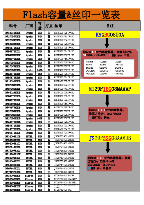
料号厂商容量打点丝印BF16G32YH0B Hynix 2GB 白H27UAG8T2BTR-BC BF27UBG5H0B Hynix 4GB 蓝H27UBG8U5ATR-BC BF27UCG5H0B Hynix 8GB 黄H27UCG8VFATR-BC BF64G26YH0B Hynix 8GB 黄H27UCG8T2MYR-BC BFBG8T25H0F Hynix 4GB 蓝H27UBG8T2BTR-BC BFBG8T25X02Hynix 4GB 蓝H27UBG8T2ATR-BC BFBG8U55H0F Hynix 4GB 蓝H27UBG8U5MTR-BC BFCG8V5MH0B Hynix 8GB 黄H27UCG8V5MTR-BC BK27UBG9H0B Hynix 4GB 蓝H27UBG8T2MYR-BC BK27UCG9H0B Hynix 8GB 黄H27UCG8UDMYR-BC BK27UDG5H0B Hynix 16GB 红H27UDG8VEMYR-BC BKAG8T25H0F Hynix 2GB 白H27UAG8T2MTR-BC BKBG8T25H1B Hynix 4GB 蓝H27UBG8T2ATR-BC BF16G32YH0B Hynix 2GB 白H27UAG8T2BTR-BC BF27UBG5H0B Hynix 4GB 蓝H27UBG8U5ATR-BC BF27UCG5H0B Hynix 8GB 黄H27UCG8VFATR-BC BF64G26YH0B Hynix 8GB 黄H27UCG8T2MYR-BC BFBG8T25H0B Hynix 4GB 蓝H27UBG8T2BTR-BC BFBG8T25X02Hynix 4GB 蓝H27UBG8T2ATR-BC BFBG8U55H0B Hynix 4GB 蓝H27UBG8U5MTR-BC BFCG8V5MH0B Hynix 8GB 黄H27UCG8V5MTR-BC BK27UBG9H0B Hynix 4GB 蓝H27UBG8T2MYR-BC BK27UCG9H0B Hynix 8GB 黄H27UCG8UDMYR-BC BK27UDG5H0B Hynix 16GB 红H27UDG8VEMYR-BC BKAG8T25H0B Hynix 2GB 白H27UAG8T2MTR-BC BKBG8T25H1B Hynix 4GB 蓝H27UBG8T2ATR-BC BNAG8T25H0B Hynix 2GB 白H27UAG8T2ATR-BC BNBG8T25H0B Hynix 4GB 蓝H27UBG8T2AYR-BC BF32G08520B INTEL 4GB 蓝JS29F32G08AAME1BF32G08DX02INTEL 4GB 蓝JS29F32G08AAMDB BF64G085202INTEL 8GB 黄JS29F64G08AAME1BF9F64G5X02INTEL 8GB 黄JS29F64G08CAMDB BFJS29F5202INTEL 2GB 白JS29F16B08CAME1BF16B08520F INTEL 2GB 白JS29F16B08JAMDB BF32G085202INTEL 4GB 蓝JS29F32G08AAME1BF32G08DX02INTEL 4GB 蓝JS29F32G08AAMDB BF64G085202INTEL 8GB 黄JS29F64G08AAME1BF9F64G5X02INTEL 8GB 黄JS29F64G08CAMDB BFJS29F5202INTEL 2GB 白JS29F16B08CAME1BF16G085M0B Micron 2GB 白MT29F16G08MAAWP BF32G083M02Micron 4GB 蓝MT29F32G08CBACAWP BF64G089M0B Micron 8GB 黄MT29F64G08CECBBH1BF64G089X0F Micron 8GB 黄MT29F64G08EBAAAB74A3WC1BK32G085M0B Micron 4GB 蓝MT29F32G08QAA BK64G085M0BMicron8GB黄MT29F64G08TAAK9G BG 08U0AFlash容量&丝印一览表备注MT 29F 16G 08MAAWPJS 29F 32G 08AAMDB标识点6.7.8位为容量换算,换算方法为:32Gb/8=4GB 16Gb=2GB 68Gb=8GB标识点4.5位为容量换算,换算方法为:BG (32Gb )/8=4GB K9指厂商:三星标识点6.7.8位为容量换算,换算方法为:16Gb/8=2GB MT 指厂商:镁光80:8M 1G:1G 2G:2G 4G:4G 8G:8G AG:16G BG:32G CG:64G ZG:48G DG:128G EG:256G GG:384G HG:512G LG:24G NG:96GBN128G8YM02Micron16GB红MT29F128G08CFAAAWP BN32G085M0B Micron4GB蓝MT29F32G08CBAAAWC BN32G085M1B Micron4GB蓝MT29F32G08CBABAWP BN32G085M2B Micron4GB蓝MT29F32G08CBACAWP BN64G085M0B Micron8GB黄MT29F64G08CFAAAWC BN64G085M12Micron8GB黄MT29F64G08CBAAAWP BN64G085M1B Micron8GB黄MT29F64G08CBAAAWP BN64G08YM0B Micron8GB黄MT29F64G08CEAAAC5 BF0GD8U5S02samsung8GB黄K9ACGD8U0MBF1G08U5S0B samsung128MB无点K9F1G08U0CBF1G08U5S0F samsung128MB无点K9F1G08U0CBF4G08U9S0F samsung512MB无点K9F4G08U0BBF8G08UDS0B samsung1GB绿K9K8G08U1DBFAG08UDS0B samsung2GB白K9FAG08U0MBFBG08U5S0B samsung4GB蓝K9GBG08U0ABFBG08U9S02samsung4GB蓝K9ABG08U0ABFG08U05X1B samsung2GB白K9GAG08U0EBFG08U05X1F samsung2GB白K9GAG08U0DBFK9ABG5S0B samsung4GB蓝K9ABGD8U0BBFK9BCGYS02samsung8GB黄K9BCG08U1ABKBG08U9S0B samsung4GB蓝K9ABG08U0ABKCG08U9S0F samsung8GB黄K9BCG08U1ABKDG08U9S0B samsung16GB红K9CDG08U5ABN04G085S0F samsung512MB无点K9F4G08U0ABNAG08UDS0B samsung2GB白K9GAG08U0MBNF2G085S0B samsung256MB无点K9F2G08U0BBNF8G085S0B samsung1GB绿K9F8G08U0M BNG4G085S0B samsung512MB无点K9G4G08U0B BNK8G08DS0B samsung1GB绿K9K8G08U0B BNKAG085S0B samsung2GB白K9KAG08U0M BF1G08U5S0B samsung128MB无点K9F1G08U0C BF4G08U9S0F samsung512MB无点K9F4G08U0B BF8G08UDS0B samsung1GB绿K9K8G08U1D BFAG08UDS0B samsung2GB白K9FAG08U0M BFBG08U5S0B samsung4GB蓝K9GBG08U0A BFBG08U9S02samsung4GB蓝K9ABG08U0A BFG08U05X1B samsung2GB白K9GAG08U0E BFG08U05X1F samsung2GB白K9GAG08U0D BFK9ABG5S02samsung4GB蓝K9ABGD8U0B BFK9BCGYS02samsung8GB黄K9BCG08U1A BKBG08U9S0B samsung4GB蓝K9ABG08U0A BKCG08U9S0B samsung8GB黄K9BCG08U1A BKDG08U9S0F samsung16GB红K9CDG08U5A BN04G085S0F samsung512MB无点K9F4G08U0A BN0K9GB5X0B samsung4GB蓝K9GBG08U0A BN0K9GB5X0B samsung4GB蓝K9GBG08U0AH27U BG8T2BTR-BC标识点5.6位为容量换算,换算方法为:BG(32Gb)/8=4GBH指厂商:海力士1G=128MB2G=256MB4G=512MB8G=1GBAG(16G)=2GBBG(32G)=4GBCG(64G)=8GBDG(128G)=16GBEG(256G)=32GBGG(384G)=48GBHG(512G)=64GBLG(24G)=3GBNG(96G)=12GBZG(48G)=6GB64:64Mb 12:128Mb25:256Mb 51:512Mb 1G:1G2G:2G 4G:4G 8G:8GAG:16G BG:32G CG:64GDG:128G EG:256G容量换算信息:。
HY27UF081G2A NAND Flash数据手册

This document is a general product description and is subject to change without notice. Hynix does not assume any responsibility for use of circuits described. No patent licenses are implied.Rev 0.4 / Jun. 2007 1HY27UF(08/16)1G2A Series1Gbit (128Mx8bit / 64Mx16bit) NAND Flash1Gb NAND FLASHHY27UF081G2A HY27UF161G2ARev 0.4 / Jun. 200721Gbit (128Mx8bit / 64Mx16bit) NAND FlashDocument Title1Gbit (128Mx8bit / 64Mx16bit) NAND Flash Memory Revision HistoryRevision No.History Draft DateRemark0.01Initial Draft.Dec. 28. 2005Preliminary0.11) Change NOP2) Change AC CharacteristicsMay. 18. 2006Preliminary0.21) Delete Memory array map 2) Change AC Characteristics3) Correct copy back function Oct. 02. 2006Preliminary0.31) Change 1Gb Package Type- FBGA package is added - Figure & dimension are changed 2) Delet PreliminaryNov. 23. 20060.41) Correct figure 19Jun. 11. 2007tOH Before 12After10tCStCEA tREA Before 253525After202520Rev 0.4 / Jun. 200731Gbit (128Mx8bit / 64Mx16bit) NAND FlashFEATURES SUMMARYHIGH DENSITY NAND FLASH MEMORIES - Cost effective solutions for mass storage applications NAND INTERFACE - x8 or x16 bus width.- Multiplexed Address/ Data- Pinout compatibility for all densitiesSUPPLY VOLTAGE- VCC = 2.7 to 3.6V : HY27UFxx1G2A Memory Cell Array= (2K+64) Bytes x 64 Pages x 1,024 Blocks = (1K+32) Bytes x 64 Pages x 1,024 BlocksPAGE SIZE- x8 device : (2K+64 spare) Bytes : HY27UF081G2A - x16 device : (1K+32 spare) Bytes : HY27UF161G2ABLOCK SIZE- x8 device: (128K + 4K spare) Bytes - x16 device: (64K + 2K spare) Words PAGE READ / PROGRAM - Random access: 25us (max.) - Sequential access: 30ns (min.) - Page program time: 200us (typ.)COPY BACK PROGRAM MODE- Fast page copy without external bufferingCACHE PROGRAM- Internal (2048+64) Byte buffer to improve the program throughputFAST BLOCK ERASE- Block erase time: 2ms (Typ.)STATUS REGISTER ELECTRONIC SIGNATURE - 1st cycle: Manufacturer Code - 2nd cycle: Device Code- 3rd cycle: Internal chip number , Cell Type, Number of Simultaneously Programmed Pages.- 4th cycle: Page size, Block size, Organization, Spare sizeSERIAL NUMBER OPTION CHIP ENABLE DON’T CARE - Simple interface sith microcontrollerDATA RETENTION- 100,000 Program/Erase cycles (with 1bit/528byte ECC) - 10 years Data RetentionPACKAGE- HY27UF(08/16)1G2A-T(P): 48-Pin TSOP1 (12 x 20 x 1.2 mm)- HY27UF(08/16)1G2A-T (Lead)- HY27UF(08/16)1G2A-TP (Lead Free)- HY27UF081G2A-S(P): 48-Pin USOP1 (12 x 17 x 0.65 mm)- HY27UF081G2A-S (Lead)- HY27UF081G2A-SP (Lead Free) - HY27UF081G2A-F(P): 63-Ball FBGA (9 x 11 x 1.0 mm)- HY27UF081G2A-F (Lead)- HY27UF081G2A-FP (Lead Free)Rev 0.4 / Jun. 200741Gbit (128Mx8bit / 64Mx16bit) NAND Flash1. SUMMARY DESCRIPTIONThe Hynix HY27UF(08/16)1G2A series is a 128Mx8bit with spare 4Mx8 bit capacity. The device is offered in 3.3V Vcc Power Supply.Its NAND cell provides the most cost-effective solution for the solid state mass storage market. The memory is divided into blocks that can be erased independently so it is possible to preserve valid data while old data is erased.The device contains 1024 blocks, composed by 64 pages consisting in two NAND structures of 32 series connected Flash cells.A program operation allows to write the 2112-byte page in typical 200us and an erase operation can be performed in typical 2ms on a 128K-byte(X8 device) block.Data in the page can be read out at 30ns cycle time per byte. The I/O pins serve as the ports for address and data input/output as well as command input. This interface allows a reduced pin count and easy migration towards different densities, without any rearrangement of footprint.Commands, Data and Addresses are synchronously introduced using CE, WE, ALE and CLE input pin. The on-chip Pro-gram/Erase Controller automates all program and erase functions including pulse repetition, where required, and inter-nal verification and margining of data.The modify operations can be locked using the WP input pin or using the extended lock block feature described later .The output pin R/B (open drain buffer) signals the status of the device during each operation. In a system with multi-ple memories the R/B pins can be connected all together to provide a global status signal.Even the write-intensive systems can take advantage of the HY27UF(08/16)1G2A extended reliability of 100K pro-gram/erase cycles by providing ECC (Error Correcting Code) with real time mapping-out algorithm.The chip could be offered with the CE don’t care function. This function allows the direct download of the code from the NAND Flash memory device by a microcontroller , since the CE transitions do not stop the read operation.The copy back function allows the optimization of defective blocks management: when a page program operation fails the data can be directly programmed in another page inside the same array section without the time consuming serial data insertion phase.The cache program feature allows the data insertion in the cache register while the data register is copied into the flash array. This pipelined program operation improves the program throughput when long files are written inside the memory. A cache read feature is also implemented. This feature allows to dramatically improve the read throughput when consecutive pages have to be streamed out.The HYNIX HY27UF(08/16)1G2A series is available in 48 - TSOP1 12 x 20 mm, 48 - USOP 12 x 17 mmm, FBGA 9 x 11 mm.1.1 Product ListPART NUMBER ORIZATIONVCC RANGE PACKAGEHY27UF081G2A x8 2.7V - 3.6 Volt63FBGA / 48TSOP1 / 48USOP1HY27UF161G2Ax1648TSOP1Rev 0.4 / Jun. 200751Gbit (128Mx8bit / 64Mx16bit) NAND FlashIO15 - IO8Data Input / Outputs (x16 only)IO7 - IO0Data Inputs / Outputs CLE Command latch enable ALE Address latch enable CE Chip Enable RE Read Enable WE Write Enable WP Write Protect R/B Ready / Busy Vcc Power Supply Vss Ground NCNo ConnectionTable 1: Signal NamesRev 0.4 / Jun. 200761Gbit (128Mx8bit / 64Mx16bit) NAND FlashFigure 2. 48TSOP1 Contactions, x8 and x16 DeviceFigure 3. 48USOP1 Contactions, x8Rev 0.4 / Jun. 200771Gbit (128Mx8bit / 64Mx16bit) NAND FlashFigure 4. 63FBGA Contactions, x8 Device (Top view through package)Rev 0.4 / Jun. 200781Gbit (128Mx8bit / 64Mx16bit) NAND Flash1.2 PIN DESCRIPTIONPin Name DescriptionIO0-IO7IO8-IO15(1)DATA INPUTS/OUTPUTSThe IO pins allow to input command, address and data and to output data during read / program operations. The inputs are latched on the rising edge of Write Enable (WE). The I/O buffer float to High-Z when the device is deselected or the outputs are disabled.CLECOMMAND LATCH ENABLEThis input activates the latching of the IO inputs inside the Command Register on the Rising edge of Write Enable (WE).ALEADDRESS LATCH ENABLEThis input activates the latching of the IO inputs inside the Address Register on the Rising edge of Write Enable (WE).CECHIP ENABLEThis input controls the selection of the device. When the device is busy CE low does not deselect the memory.WEWRITE ENABLEThis input acts as clock to latch Command, Address and Data. The IO inputs are latched on the rise edge of WE.REREAD ENABLEThe RE input is the serial data-out control, and when active drives the data onto the I/O bus. Data is valid tREA after the falling edge of RE which also increments the internal column address counter by one.WP WRITE PROTECTThe WP pin, when Low, provides an Hardware protection against undesired modify (program / erase)operations.R/B READY BUSYThe Ready/Busy output is an Open Drain pin that signals the state of the memory.VCC SUPPLY VOLTAGEThe VCC supplies the power for all the operations (Read, Write, Erase). VSS GROUNDNCNO CONNECTIONTable 2: Pin DescriptionNOTE:1. A 0.1uF capacitor should be connected between the Vcc Supply Voltage pin and the Vss Ground pin to decouple the current surges from the power supply. The PCB track widths must be sufficient to carry the currents required during program and erase operations.Rev 0.4 / Jun. 200791Gbit (128Mx8bit / 64Mx16bit) NAND FlashIO0IO1IO2IO3IO4IO5IO6IO71st Cycle A0A1A2A3A4A5A6A72nd Cycle A8A9A10A11L (1)L (1)L (1)L (1)3rd Cycle A12A13A14A15A16A17A18A194th CycleA20A21A22A23A24A25A26A27Table 3: Address Cycle Map(x8)NOTE:1. L must be set to Low.IO0IO1IO2IO3IO4IO5IO6IO7IO8-IO151st Cycle A0A1A2A3A4A5A6A7L (1)2nd Cycle A8A9A10L (1)L (1)L (1)L (1)L (1)L (1)3rd Cycle A11A12A13A14A15A16A17A18L (1)4th CycleA19A20A21A22A23A24A25A26L (1)Table 4: Address Cycle Map(x16)NOTE:1. L must be set to Low.FUNCTION1st CYCLE2nd CYCLE3rd CYCLE4th CYCLEAcceptable commandduring busyREAD 100h 30h --READ FOR COPY-BACK 00h 35h --READ ID 90h ---RESETFFh ---YesPAGE PROGRAM 80h 10h --COPY BACK PGM 85h 10h --BLOCK ERASE60h D0h --READ STATUS REGISTER 70h ---YesCACHE PROGRAM 80h 15h --RANDOM DATA INPUT 85h ---RAMDOM DATA OUTPUT 05h E0h --CACHE READ START 00h 31h --CACHE READ EXIT34h---Table 5: Command SetRev 0.4 / Jun. 2007101Gbit (128Mx8bit / 64Mx16bit) NAND FlashCLE ALE CE WE RE WP MODE H L L Rising H X Read ModeCommand Input L H L Rising H X Address Input(4 cycles)H L L Rising H H Write ModeCommand Input L H L Rising H HAddress Input(4 cycles)L L L Rising H H Data Input L L L (1)H Falling X Sequential Read and Data Output L L L H H X During Read (Busy)X X X X X H During Program (Busy)X X X X X HDuring Erase (Busy)X X X X X L Write Protect XXHXX0V/Vcc Stand ByTable 6: Mode SelectionNOTE:1. With the CE high during latency time does not stop the read operationRev 0.4 / Jun. 2007111Gbit (128Mx8bit / 64Mx16bit) NAND Flash2. BUS OPERATIONThere are six standard bus operations that control the device. These are Command Input, Address Input, Data Input, Data Output, Write Protect, and Standby.Typically glitches less than 5 ns on Chip Enable, Write Enable and Read Enable are ignored by the memory and do not affect bus operations.2.1 Command Input.Command Input bus operation is used to give a command to the memory device. Command are accepted with Chip Enable low, Command Latch Enable High, Address Latch Enable low and Read Enable High and latched on the rising edge of Write Enable. Moreover for commands that starts a modify operation (write/erase) the Write Protect pin must be high. See figure 6 and table 13 for details of the timings requirements. Command codes are always applied on IO7:0, disregarding the bus configuration (X8/X16).2.2 Address Input.Address Input bus operation allows the insertion of the memory address. To insert the 28 addresses needed to access the 1Gbit 4 clock cycles (x8 version) are needed. Addresses are accepted with Chip Enable low, Address Latch Enable High, Command Latch Enable low and Read Enable High and latched on the rising edge of Write Enable. Moreover for commands that starts a modify operation (write/erase) the Write Protect pin must be high. See figure 7 and table 16 for details of the timings requirements. Addresses are always applied on IO7:0, disregarding the bus configuration (X8/X16).2.3 Data Input.Data Input bus operation allows to feed to the device the data to be programmed. The data insertion is serially and timed by the Write Enable cycles. Data are accepted only with Chip Enable low, Address Latch Enable low, Command Latch Enable low, Read Enable High, and Write Protect High and latched on the rising edge of Write Enable. See figure 8 and table 13 for details of the timings requirements.2.4 Data Output.Data Output bus operation allows to read data from the memory array and to check the status register content, the lock status and the ID data. Data can be serially shifted out toggling the Read Enable pin with Chip Enable low, Write Enable High, Address Latch Enable low, and Command Latch Enable low. See figures 9,10,12,13 and table 13 for details of the timings requirements.2.5 Write Protect.Hardware Write Protection is activated when the Write Protect pin is low. In this condition modify operation do not start and the content of the memory is not altered. Write Protect pin is not latched by Write Enable to ensure the pro-tection even during the power up.2.6 Standby.In Standby mode the device is deselected, outputs are disabled and Power Consumption is reduced.Rev 0.4 / Jun. 2007121Gbit (128Mx8bit / 64Mx16bit) NAND Flash3. DEVICE OPERATION3.1 Page Read.Upon initial device power up, the device defaults to Read mode. This operation is also initiated by writing 00h and 30h to the command register along with four address cycles. In two consecutive read operations, the second one does need 00h command, which four address cycles and 30h command initiates that operation. Second read operation always requires setup command if first read operation was executed using also random data out command.Two types of operations are available: random read. The random read mode is enabled when the page address is changed. The 2112 bytes (X8 device) or 1056 words (X16 device) of data within the selected page are transferred to the data registers in less than 25us(tR). The system controller may detect the completion of this data transfer (tR) by analyzing the output of R/B pin. Once the data in a page is loaded into the data registers, they may be read out in 30ns cycle time (3.3V device) by sequentially pulsing RE. The repetitive high to low transitions of the RE clock make the device output the data starting from the selected column address up to the last column address.The device may output random data in a page instead of the consecutive sequential data by writing randomdata output command. The column address of next data, which is going to be out, may be changed to the address which follows random data output command.Random data output can be operated multiple times regardless of how many times it is done in a page.Random data output is not available in cache read.3.2 Page Program.The device is programmed basically by page, but it does allow multiple partial page programming of a word or consec-utive bytes up to 2112 (X8 device) or words up to 1056 (X16 device), in a single page program cycle.The number of consecutive partial page programming operation within the same page without an intervening erase operation must not exceed 8; for example, 4 times for main array (X8 device:1time/512byte, X16 device:1time 256word) and 4 times for spare array (X8 device:1time/16byte ,X16 device:1time/8word).The addressing should be done in sequential order in a block. A page program cycle consists of a serial data loading period in which up to 2112 bytes (X8 device) or 1056 words (X16 device) of data may be loaded into the data register , followed by a non-volatile programming period where the loaded data is programmed into the appropriate cell.The serial data loading period begins by inputting the Serial Data Input command (80h), followed by the four cycle address inputs and then serial data. The words other than those to be programmed do not need to be loaded. The device supports random data input in a page. The column address of next data, which will be entered, may bechanged to the address which follows random data input command (85h). Random data input may be operated multi-ple times regardless of how many times it is done in a page.The Page Program confirm command (10h) initiates the programming process. Writing 10h alone without previously entering the serial data will not initiate the programming process. The P/E/R controller automatically executes the algorithms and timings necessary for program and verify, thereby freeing the system controller for other tasks. Once the program process starts, the Read Status Register command may be entered to read the status register . The system controller can detect the completion of a program cycle by monitoring the R/B output, or the Status bit (I/O 6) of the Status Register . Only the Read Status command and Reset command are valid while programming is in progress. When the Page Program is complete, the Write Status Bit (I/O 0) may be checked. The internal write verify detects only errors for "1"s that are not successfully programmed to "0"s. The command register remains in Read Status command mode until another valid command is written to the command register . Figure 14 details the sequence.Rev 0.4 / Jun. 2007131Gbit (128Mx8bit / 64Mx16bit) NAND Flash3.3 Block Erase.The Erase operation is done on a block basis. Block address loading is accomplished in two cycles initiated by an Erase Setup command (60h). Only address A18 to A27 (X8) or A17 to A26 (X16) is valid while A12 to A17 (X8) or A11 to A16 (X16) are ignored. The Erase Confirm command (D0h) following the block address loading initiates the internal erasing process. This two-step sequence of setup followed by execution command ensures that memory contents are not acci-dentally erased due to external noise conditions. At the rising edge of WE after the erase confirm command input, the P/E/R controller handles erase and erase-verify. Once the erase process starts, the Read Status Register command may be entered to read the status register . The system controller can detect the completion of an erase by monitoring the R/B output, or the Status bit (I/O 6) of the Status Register . Only the Read Status command and Reset command are valid while erasing is in progress. When the erase operation is completed, the Write Status Bit (I/O 0) may be checked. Figure 18 details the sequence.3.4 Copy-Back Program.The copy-back program is configured to quickly and efficiently rewrite data stored in one page without utilizing an exter-nal memory. Since the time-consuming cycles of serial access and re-loading cycles are removed, the system perfor-mance is improved. The benefit is especially obvious when a portion of a block is updated and the rest of the block also need to be copied to the newly assigned free block. The operation for performing a copy-back program is a sequential execution of page-read without serial access and copyingprogram with the address of destination page. A read opera-tion with "35h" command and the address of the source page moves the whole 2112byte (X8 device) or 1056word (X16 device) data into the internal data buffer .As soon as the device returns to Ready state, Copy Back command (85h) with the address cycles of destination page may be written. The Program Confirm command (10h) is required to actually begin the programming operation. Data input cycle for modifying a portion or multiple distant portions of the source page is allowed as shown in Figure 16."When there is a program-failure at Copy-Back operation, error is reported by pass/fail status. But, if Copy-Back operations are accumulated over time, bit error due to charge loss is not checked by external error detection/correction scheme. For this reason, two bit error correction is recommended for the use of Copy-Back operation."Figure 16 shows the command sequence for the copy-back operation.The Copy Back Program operation requires three steps:1. The source page must be read using the Read A command (one bus write cycle to setup the command and then 4 bus write cycles to input the source page address). This operation copies all 2KBytes from the page into the Page Buffer .2. When the device returns to the ready state (Ready/Busy High), the second bus write cycle of the command is given with the 4bus cycles to input the target page address.3. Then the confirm command is issued to start the P/E/R Controller .Note:1. On the same plane.2. It’s prohibited to operate copy-back program from an odd address page (source page) to an even address page (target page) or from an even address page (source page) to an odd address page (target page). Therefore, the copy-back program is permitted just between odd address pages or even address pages.Rev 0.4 / Jun. 2007141Gbit (128Mx8bit / 64Mx16bit) NAND Flash3.5 Read Status Register.The device contains a Status Register which may be read to find out whether read, program or erase operation is com-pleted, and whether the program or erase operation is completed successfully. After writing 70h command to the com-mand register , a read cycle outputs the content of the Status Register to the I/O pins on the falling edge of CE or RE, whichever occurs last. This two line control allows the system to poll the progress of each device in multiple memory connections even when R/B pins are common-wired. RE or CE does not need to be toggled for updated status. Refer to Table 14 for specific Status Register definitions, and Figure 10 for specific timings requirements . The command reg-ister remains in Status Read mode until further commands are issued to it. Therefore, if the status register is read dur-ing a random read cycle, the read command (00h) should be given before starting read cycles.3.6 Read ID.The device contains a product identification mode, initiated by writing 90h to the command register , followed by an address input of 00h. Four read cycles sequentially output the 1st cycle (ADh), and 2nd cycle (the device code) and 3rd cycle ID, 4th cycle ID, respectively. The command register remains in Read ID mode until further commands are issued to it. Figure 19 shows the operation sequence, while Tables 16 explain the byte meaning.3.7 Reset.The device offers a reset feature, executed by writing FFh to the command register . When the device is in Busy state during random read, program or erase mode, the reset operation will abort these operations. The contents of memory cells being altered are no longer valid, as the data will be partially programmed or erased.The command register is cleared to wait for the next command, and the Status Register is cleared to value E0h when WP is high. Refer to table 14 for device status after reset operation. If the device is already in reset state a new reset command will not be accepted by the command register . The R/B pin transitions to low for tRST after the Reset com-mand is written.Rev 0.4 / Jun. 2007151Gbit (128Mx8bit / 64Mx16bit) NAND Flash3.8 Cache programCache Program is an extension of Page Program, which is executed with 2112byte (X8 device) or 1056word (X16 device) data registers, and is available only within a block. Since the device has 1 page of cache memory, serial data input may be executed while data stored in data register are programmed into memory cell. After writing the first set of data up to 2112byte (X8 device) or 1056word (X16 device) into the selected cache registers, Cache Program com-mand (15h) instead of actual Page Program (10h) is input to make cache registers free and to start internal program operation. To transfer data from cache registers to data registers, the device remains in Busy state for a short period of time (tCBSY) and has its cache registers ready for the next data-input while the internal programming gets started with the data loaded into data registers. Read Status command (70h) may be issued to find out when cache registers become ready by polling the Cache- Busy status bit (I/O 6). Pass/fail status of only the previous page is available upon the return to Ready state.When the next set of data is input with the Cache Program command, tCBSY is affected by the progress of pending internal programming. The programming of the cache registers is initiated only when the pending program cycle is finished and the data registers are available for the transfer of data from cache registers. The status bit (I/O5) for internal Ready/Busy may be polled to identify the completion of internal programming.If the system monitors the progress of programming only with R/B, the last page of the target programming sequence must be programmed with actual Page Program command (10h). If the Cache Program command (15h) is used instead, status bit (I/O5) must be polled to find out when the last programming is actually finished before starting other operations such as read. Pass/fail status is available in two steps. I/O 1 returns with the status of the previous page upon Ready or I/O6 status bit changing to "1", and later I/O 0 with the status of current page upon true Ready (returning from internal programming) or I/O 5 status bit changing to "1". I/O 1 may be read together when I/O 0 is checked. See Fig. 18 for more details.NOTE : Since programming the last page does not employ caching, the program time has to be that of Page Program. However , if the previous program cycle with the cache data has not finished, the actual program cycle of the last page is initiated only after completion of the previous cycle, which can be expressed as the following formula.tPROG=Program time for the last page + Program time for the (last-1)page - (Program command cycle time + Last page data loading time)Rev 0.4 / Jun. 2007161Gbit (128Mx8bit / 64Mx16bit) NAND Flash3.9 Cache ReadCache read operation allows automatic download of consecutive pages, up to the whole device. Immediately after 1st latency end, while user can start reading out data, device internally starts reading following page.Start address of 1st page must be at page start (A<10:0>=00h) : in this way after 1st latency time (tr) , automatic data download will be uninterrupted. In fact latency time is 25us, while download of a page require at least 100us for x8 device (50us for x16 device).Cache read operation command is like standard read, except for confirm code (30h for standard read, 31h for cache read) user can check operation status using :- R/B ( ‘0’ means latency ongoing, download not possible, ‘1’ means download of n page possible, even if device in ternally is active on n+1 page- Status register (SR<6> behave like R/B, SR<5> is ‘0’ when device is internally reading and ‘1’ when device is idle)To exit cache read operation, a cache read exit command (34h) must be issued. This command can be given any time (both device idle and reading).If device is active (SR<5>=0) it will go idle within 5us, while if it is not active, device itself will go busy for a time shorter then tCBSY before becoming again idle and ready to accept any further commands. Figure 17 describes how to handle Cache Read through Status register .If user reads last byte/word of the memory array, then he has to stop by giving a cache read exit command. In general,if user wants to terminate a cache read, then he must give a cache read exit command (or reset command) before starting any new operation.Random data output is not available in cache read.Cache read operation must be done only block by block if system needs to avoid reading also from invalid blocks.Rev 0.4 / Jun. 2007171Gbit (128Mx8bit / 64Mx16bit) NAND Flash4. OTHER FEATURES4.1 Data Protection for Power on/off SequenceThe device is designed to offer protection from any involuntary program/erase during power-transitions. An internal voltage detector disables all functions whenever Vcc is below about 2.0V (3.3V version). WP pin provides hardware protection and is recommended to be kept at VIL during power-up and power-down. A recovery time of minimum 10us is required before internal circuit gets ready for any command sequences as shown in Figure 24. The two-step com-mand sequence for program/erase provides additional software protection.If the power is dropped during the ready read/write/erase operation, Power protection function may not guaranteed the data. Power protection function is only available during the power on/off sequence.4.2 Ready/Busy.The device has a Ready/Busy output that provides method of indicating the completion of a page program, erase, copy-back, cache program and random read completion. The R/B pin is normally high and goes to low when the device is busy (after a reset, read, program, erase operation). It returns to high when the P/E/R controller has finished the operation. The pin is an open-drain driver thereby allowing two or more R/B outputs to be Or-tied. Because pull-up resistor value is related to tr(R/B) and current drain during busy (Ibusy), an appropriate value can be obtained with the following reference chart (Figure 25). Its value can be determined by the following guidance.。
flash芯片选型
flash芯片选型Flash芯片是一种常见的存储器件,它可以在断电后仍然保持数据的存储状态。
在现代电子产品中,Flash芯片几乎无处不在,用于存储各种程序、文件和数据。
选择合适的Flash芯片对于设计电子产品至关重要,关系到产品的性能、稳定性和成本。
以下是一些选型Flash芯片的要点,以帮助您做出明智的选择。
1.存储容量:根据产品的需求确定所需的存储容量。
不同的应用场景可能需要不同容量的存储空间。
注意,Flash芯片的存储容量通常以字节(B)计算,常见的容量有128MB、256MB、512MB、1GB、2GB等。
2.接口类型:根据产品的主控芯片确定所需的接口类型。
常见的接口类型有SPI、SDIO、NAND、NOR等。
SPI接口适用于小容量的应用,SDIO接口适用于需要高速数据传输的应用,NAND接口适用于大容量存储器,NOR接口适用于需要较高可靠性和速度的应用。
3.速度等级:根据产品对读写速度的要求确定所需的速度等级。
速度等级通常以MHz表示,常见的等级有25MHz、50MHz、100MHz等。
较高的速度等级可以提高数据传输速度,但也可能导致产品成本的增加。
4.工作电压:根据产品对工作电压的要求确定所需的工作电压范围。
常见的工作电压范围有1.8V、3.3V等。
选择适合产品的工作电压范围可以保证产品的稳定性和可靠性。
5.数据保持能力:Flash芯片的数据保持能力是指在断电情况下,数据可以保持的时间。
根据产品的需求确定所需的数据保持能力。
一般来说,数据保持能力越长,产品的可靠性就越高。
6.耐用性和擦写次数:Flash芯片通常具有一定的擦写次数限制。
根据产品的需求确定所需的耐用性和擦写次数。
对于需要频繁写入和擦除数据的应用,选择具有更高耐用性和擦写次数的Flash芯片可以延长产品的使用寿命。
7.成本:根据产品的预算确定所需的成本范围。
不同品牌和型号的Flash芯片价格差异很大,根据产品需求在合适的价格范围内选购Flash芯片。
各家存储器性能比较

CSF 16MBit
-
64MBit-1GBit
三星samsung
现代Hynix STC ST ISSI蕊盛 旺宏 SST超捷 Ramtron intel
RAM DDR SDRAM
DDR2 SDRAM
SDR SDRAM
128MBit-2GBit
256MBit-1GBit
128MBit-1GBit
1GBit-16GBit
-
-
STC
-
-
-
ST ISSI蕊盛 旺宏 SST超捷
128MBit-1GBit
4MBit
-
-
-
-
-
-
1MBit-64MBit(Industry-Standard Flash)
512KBit-64MBit(Serial Flash)
MTP 64KBit-4MBit MPF 512KBit-64MBit MPF+
32Kit-1MBit
-
36MBit
-
256KBit-32MBit -
2MBit-72MBit -
256KBit-16MBit 1MBit-36MBit -
1MBit-4MBit -
64KBit-18MBit -
MCP
128MBit+64MBit-256MBit+128MBit NOR Only
256MBit+256MBit-2GBit+1GBit NAND Only
16MBit-1GBit
16MBit-4GBit
-
-
-
-
4MBit-256MBit
-
-
nandflash及闪存命名规则大全(三星,海力士,美光等)U盘存储技术

nandflash及闪存命名规则大全(三星,海力士,美光等)U盘存储技术nandflash命名规则大全(三星,海力士,美光等)今天找三星闪存资料,发现了他的命名规则,发上来与大家分享下.三星的pure nand flash(就是不带其他模块只是nand flash存储芯片)的命名规则如下:1. Memory (K)2. NAND Flash : 93. Small Classification(SLC : Single Level Cell, MLC : Multi Level Cell,SM : SmartMedia, S/B : Small Block)1 : SLC 1 Chip XD Card2 : SLC 2 Chip XD Card4 : SLC 4 Chip XD CardA : SLC + Muxed I/ F ChipB : Muxed I/ F ChipD : SLC Dual SME : SLC DUAL (S/ B)F : SLC NormalG : MLC NormalH : MLC QDPJ : Non-Muxed OneNandK : SLC Die StackL : MLC DDPM : MLC DSPN : SLC DSPQ : 4CHIP SMR : SLC 4DIE STACK (S/ B)S : SLC Single SMT : SLC SINGLE (S/ B)U : 2 STACK MSPV : 4 STACK MSPW : SLC 4 Die Stack4~5. Density(注:实际单位应该是bit,而不是Byte)12 : 512M16 : 16M28 : 128M32 : 32M40 : 4M56 : 256M64 : 64M80 : 8M1G : 1G2G : 2G4G : 4G8G : 8GAG : 16GBG : 32GCG : 64GDG : 128G00 : NONE6~7. organization00 : NONE08 : x816 : x168. VccA : 1.65V~3.6VB : 2.7V (2.5V~2.9V)C : 5.0V (4.5V~5.5V)D : 2.65V (2.4V ~ 2.9V)E : 2.3V~3.6VR : 1.8V (1.65V~1.95V)Q : 1.8V (1.7V ~ 1.95V)T : 2.4V~3.0VU : 2.7V~3.6VV : 3.3V (3.0V~3.6V)W : 2.7V~5.5V, 3.0V~5.5V0 : NONE9. Mode0 : Normal1 : Dual nCE & Dual R/ nB4 : Quad nCE & Single R/ nB5 : Quad nCE & Quad R/ nB9 : 1st block OTPA : Mask Option 1L : Low grade10. GenerationM : 1st GenerationA : 2nd GenerationB : 3rd GenerationC : 4th GenerationD : 5th Generation11. "─"12. PackageA : COBB : TBGAC : CHIP BIZD : 63-TBGAE : TSOP1 (Lead-Free, 1217)F : WSOP (Lead-Free)G : FBGAH : TBGA (Lead-Free)I : ULGA (Lead-Free)J : FBGA (Lead-Free)K : TSOP1 (1217)L : LGAM : TLGAN : TLGA2P : TSOP1 (Lead-Free)Q : TSOP2 (Lead-Free)R : TSOP2-RS : SMART MEDIAT : TSOP2U : COB (MMC)V : WSOPW : WAFERY : TSOP113. TempC : CommercialI : IndustrialS : SmartMediaB : SmartMedia BLUE0 : NONE (Containing Wafer, CHIP, BIZ, Exception handling code)3 : Wafer Level 314. Bad BlockA : Apple Bad BlockB : Include Bad BlockD : Daisychain SampleK : Sandisk BinL : 1~5 Bad BlockN : ini. 0 blk, add. 10 blkS : All Good Block0 : NONE (Containing Wafer, CHIP, BIZ, Exceptionhandling code)15. NAND-Reserved0 : Reserved16. Packing Type- Common to all products, except of Mask ROM- Divided into TAPE & REEL(In Mask ROM, divided into TRAY, AMMO Packing Separately)【举例说明】K 9 G A G 0 8 U 0 M - P C B 01 2 3 4 5 6 7 8 9 10 11 12 13 14 1 5 16 17 18K9GAG08U0M 详细信息如下:1. Memory (K)2. NAND Flash : 93. Small Classification(SLC : Single Level Cell, MLC : Multi Level Cell,SM : SmartMedia, S/B : Small Block)G : MLC Normal4~5. DensityAG : 16G (Note: 这里单位是bit而不是byte,因此实际大小是16Gb=2GB)6. Technology0 : Normal (x8)7. Organization0 : NONE 8 : x88. VccU : 2.7V~3.6V9. Mode0 : Normal10. GenerationM : 1st Generation11. "─"12. PackageP : TSOP1 (Lead-Free)13. TempC : Commercial14. Customer Bad BlockB : Include Bad Block15. Pre-Program Version0 : None整体描述就是:K9GAG08U0M是,三星的MLC Nand Flash,工作电压为2.7V~3.6V,x8(即I/O是8位),大小是2GB(16Gb),TSOP1封装。
Hynix NAND flash型号指南
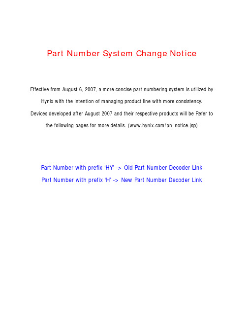
Part Number System Change NoticeEffective from August 6, 2007, a more concise part numbering system is utilized by Hynix with the intention of managing product line with more consistency. Devices developed after August 2007 and their respective products will be Refer to the following pages for more details. (/pn_notice.jsp)Part Number with prefix ‘HY’ -> Old Part Number Decoder LinkPart Number with prefix ‘H’ -> New Part Number Decoder LinkH 2 7 X X X X X X X X X - X X(1) HYNIX(2) PRODUCT FAMILY(4) POWER SUPPLY(V CC )(8) NAND CLASSIFICATION(7) ORGANIZATION(14) BAD BLOCK(11) PACKAGE TYPE2: FlashS A B F G H J K T U V W Y : SLC + Single Die + Small Block : SLC + Double Die + Small Block : SLC + Quadruple Die + Small Block : SLC + Single Die + Large Block : SLC + Double Die + Large Block : SLC + Quadruple Die + Large Block : SLC + ODP + Large Block : SLC + DSP + Large Block: MLC + Single Die + Large Block : MLC + Double Die + Large Block : MLC + Quadruple Die + Large Block : MLC + DSP + Large Block : MLC + ODP + Large BlockC E M IB S P : Included Bad Block: 1~5 Bad Block Included : All Good BlockT V S N F X M Y U W C K D : TSOP1: WSOP : USOP : LSOP1: FBGA : LGA : WLGA : VLGA : ULGA : Wafer: PGD1 (chip): KGD : PGD2: 1st : 2nd : 3rd : 4thM A B C (5), (6) DENSITY1245D F : 1 nCE & 1 R/nB; Sequential Row Read Enable : 1 nCE & 1 R/nB; Sequential Row Read Disable : 2 nCE & 2 R/nB; Sequential Row Read Enable : 2 nCE & 2 R/nB; Sequential Row Read Disable : Dual Interface; Sequential Row Read Disable : 4 nCE & 4 R/nB ; Sequential Row Read Disable(12) PACKAGE MATERIALA P L R : Wafer : Lead Free : Leaded: Lead & Halogen Free(1)(4)(2)(3)(5)(7)(6)(9)(15)NAND Flash PART NUMBERING(8)(10)(11)(12)(14)(13)(3) PRODUCT MODE7: NAND FlashU L S : 2.7V~3.6V : 2.7V : 1.8V64251G 4G AG CG : 64Mb : 256Mb : 1Gb : 4Gb : 16Gb : 64Gb12512G 8G BG DG: 128Mb : 512Mb : 2Gb : 8Gb : 32Gb : 128Gb86: x8: x16(10) DIE GENERATION(9) FUNCTION MODE: Commercial (0℃~70℃): Extended (-25℃~85℃): Mobile (-30℃~85℃): Industrial (-40℃~85℃)(13) - d“ - ”(15) OPERATIONTEMPERATUREHY XX X X XX XX X X - X (X) (X) (X) (X)(1) HYNIX MEMORY(2) COMPONENT GROUP(3) POWER SUPPLY(V CC )(4) CLASSIFICATION(5) BIT ORGANIZATION(11) OPERATING TEMPERATURE(12) BAD BLOCK(9) PACKAGE TYPE(8) VERSION: 2.7V~3.6V : 2.7V : 1.8V27: NAND FlashU L S S A B F G H K T U V W : SLC + Single Die + S/B : SLC + Double Die + S/B : SLC + Quadruple Die + S/B : SLC + Single Die + L/B : SLC + Double Die + L/B : SLC + Quadruple Die + L/B : SLC + DSP + L/B: MLC + Single Die + L/B : MLC + Double Die + L/B : MLC + Quadruple Die + L/B : MLC + DSP + L/B081632: x8: x16: x32Blank C E M I: Wafer , Chip : 0℃~70℃: -25℃~85℃: -30℃~85℃: -40℃~85℃Blank B S P : Wafer: Included Bad Block : 1~5 Bad Block : All Good BlockT V S E F B G H U Y M W C K D : TSOP1: WSOP : USOP : WELP: FBGA(63ball): FBGA(107ball): FBGA(149ball): TBGA : ULGA : VLGA : WLGA : Wafer : Chip : KGD : PGD2: 1st Gen.: 2nd Gen.: 3rd Gen.: 4th Gen.: Down Density(1st): Down Density(2nd)M A B C 12(6) DENSITY64561G 4G AG CG ZG : 64Mb : 256Mb : 1Gb : 4Gb : 16Gb : 64Gb : 48Gb(7) MODE12456789D F T : 1 nCE & 1 R/nB; Sequential Row Read Enable : 1 nCE & 1 R/nB; Sequential Row Read Disable : 2 nCE & 2 R/nB; Sequential Row Read Enable : 2 nCE & 2 R/nB; Sequential Row Read Disable: 1 nCE & 1 R/nB; Sequential Row Read Enable & Auto Read Page 0: 2 nCE & 2 R/nB; Sequential Row Read Enable & Auto Read Page 0: 1 nCE & 1 R/nB; Sequential Row Read Disable & Auto Read Page 0: 2 nCE & 2 R/nB; Sequential Row Read Disable & Auto Read Page 0: Dual Interface; Sequential Row Read Disable : 4 nCE & 4 R/nB ; Sequential Row Read Disable : 3 nCE & 3 R/nB ; Sequential Row Read Disable(13) OPTION(CUSTOMER)Customer Initial Option(10) PACKAGE MATERIALBlank P H R : Normal, Wafer , Chip, KGD : Lead Free : Halogen Free: Lead & Halogen Free(1)(3)(2)(4)(6)(5)(7)(9)(8)(11)(10)(12)(13)NAND Flash PART NUMBERING28122G 8G BG DG : 128Mb : 512Mb : 2Gb : 8Gb : 32Gb : 128Gb。
NandFlash和NorFlash详解
Flash Nor Nand闪存简介:闪存是可通过电擦写和重编程的非挥发性计算机存储器。
闪存技术主要应用在计算机和其他数字设备间传输数据的存储卡和USB盘上。
它是一种可用大块擦写和重编程技术访问的特殊类型的EEPROM (Electrically Erasable Programmable Read-Only Memory)。
闪存不需要电源维持芯片内保存的数据。
另外闪存相比硬盘有数倍的访问速度并且更抗震动。
它可以经受很大的压力,极端的温度,甚至可以浸泡在水中仍然保持可用。
FLASH MEMORY主要采用两种规格的技术:NAND和NOR。
NOR型与NAND型闪存的区别很大,打个比方说,NOR型闪存更像内存,有独立的地址线和数据线,但价格比较贵,容量比较小;而NAND型更像硬盘,地址线和数据线是共用的I/O线,类似硬盘的所有信息都通过一条硬盘线传送一般,而且NAND型与NOR型闪存相比,成本要低一些,而容量大得多。
因此,NOR型闪存比较适合频繁随机读写的场合,通常用于存储程序代码并直接在闪存内运行,手机就是使用NOR型闪存的大户,所以手机的“内存”容量通常不大;NAND型闪存主要用来存储资料,我们常用的闪存产品,如闪存盘、数码存储卡都是用NAND型闪存。
在大部分应用中都采用NAND FLASH,以下的芯片选型都是关于NAND FLASH。
NAND型闪存的技术特点:内存和NOR型闪存的基本存储单元是bit,用户可以随机访问任何一个bit的信息。
而NAND型闪存的基本存储单元是页(Page)(可以看到,NAND型闪存的页就类似硬盘的扇区,硬盘的一个扇区也为512字节)。
每一页的有效容量是512字节的倍数。
所谓的有效容量是指用于数据存储的部分,实际上还要加上16字节的校验信息,因此我们可以在闪存厂商的技术资料当中看到“(512+16)Byte”的表示方式。
目前2Gb以下容量的NAND型闪存绝大多数是(512+16)字节的页面容量,2Gb以上容量的NAND型闪存则将页容量扩大到(2048+64)字节。
- 1、下载文档前请自行甄别文档内容的完整性,平台不提供额外的编辑、内容补充、找答案等附加服务。
- 2、"仅部分预览"的文档,不可在线预览部分如存在完整性等问题,可反馈申请退款(可完整预览的文档不适用该条件!)。
- 3、如文档侵犯您的权益,请联系客服反馈,我们会尽快为您处理(人工客服工作时间:9:00-18:30)。
Q1’2011 DATABOOKRev 0.1NAND Flash –SLC / MLC / TLCAND FlashNNAND Flash SLC COMPONENTProduct Tech Density Block Size Stack Vcc/Org Package AvailabilityRemarkHY27US08281A 90nm 128Mb 16KB Mono 3.3v/X8TSOP/USOP Now HY27US08561A 90nm 256Mb 16KB Mono 3.3v/X8TSOP/USOP/FBGA Now HY27US08121B 70nm 512Mb 16KB Mono 3.3v/X8TSOP/USOP/FBGANow H27U518S2C 57nm 512Mb 16KB Mono 3.3v/X8TSOP Now HY27US081G1M 70nm 1Gb 16KB Mono 3.3v/X8USOPNow HY27UF081G2A 70nm 1Gb 128KB Mono 3.3v/X8TSOP/USOP/FBGANow HY27US081G2A 70nm 1Gb 128KB Mono 1.8v/X8FBGA Now H27U1G8F2B 48nm 1Gb 128KB Mono 3.3v/X8TSOP,FBGA Now H27U1G8F2B 48nm 1Gb 128KB Mono 1.8v/X8FBGA Now H27U1G8F2CTR 32nm 1Gb 128KB Mono 1.8v/X8TSOP Q4 '11H27U1G8F2CFR 32nm 1Gb 128KB Mono 1.8v/X8FBGA Q4 '11HY27UF082G2B 57nm 2Gb 128KB Mono 3.3v/X8TSOP,FBGA, LGANow H27U2G8F2C 41nm 2Gb 128KB Mono 3.3v/X8TSOP Now HY27UF084G2B 57nm 4Gb 128KB Mono 3.3v/X8TSOP Now H27U4G8F2D 41nm 4Gb 128KB Mono 3.3v/X8TSOP Now HY27UG088G5(D)B 57nm 8Gb 128KB DDP 3.3v/X8TSOP Now 2CE/Dual CH.H27U8G8G5D 41nm 8Gb 128KB Mono 3.3v/X8TSOP Now H27QBG8GDAIR-BCB 32nm 32Gb 512KB DDP 1.8v/x8VFBGA Now 2CE/Dual CH.H27QCG8HEAIR-BCB 32nm 64Gb 512KB QDP 1.8v/x8VFBGA Now 4CE/Dual CH.H27QDG8JEAJR-BCB32nm128Gb512KBODP1.8v/x8JFBGAFeb. '114CE/Dual CH.NAND Flash MLC COMPONENTProduct Tech Density Block Size Stack Vcc/Org Package AvailabilityRemarkH27U8G8T2B 48nm 8Gb 512KB Mono 3.3v/X8TSOP Now H27UAG8T2M 48nm 16Gb 512KB(4KB Page)Mono 3.3v/X8TSOP/VLGA Now H27UAG8T2A 41nm 16Gb 512KB(4KB Page)Mono 3.3v/X8TSOP Now H27UBG8U5A 41nm 32Gb 512KB(4KB Page)DDP 3.3v/X8TSOP Now H27UBG8T2M 41nm 32Gb 512KB(4KB Page)Mono 3.3v/X8VLGA Now H27UBG8T2A 32nm 32Gb 2MB(8KB Page)SDP 3.3v/x8TSOP / VLGANow H27UCG8VFA 41nm 64Gb 512KB(4KB Page)QDP 3.3v/X8TSOP Now H27UCG8UDM 41nm 64Gb 512KB(4KB Page)DDP 3.3v/X8VLGA Now Dual CH.H27UCG8U5(D)A 32nm 64Gb 2MB(8KB Page)DDP 3.3v/x8TSOP / VLGANow Dual CH. LGA H27UCG8T2M 26nm 64Gb 2MB(8KB Page)SDP 3.3v/x8VLGA Now H27UDG8VEM 41nm 128Gb 512KB(4KB Page)QDP 3.3v/X8VLGA Now 4CE,Dual CH.H27UDG8V5(E)A 32nm 128Gb 2MB(8KB Page)QDP 3.3v/x8TSOP / VLGANow 4CE,Dual CH.H27UEG8YEA 32nm 256Gb 2MB(8KB Page)ODP 3.3v/x8VLGA Now 4CE,Dual CH.H27UAG8T2B 32nm 16Gb 2MB(8KB Page)SDP 3.3v/x8TSOP Now H27UBG8T2B 26nm 32Gb 2MB(8KB Page)SDP 3.3v/x8TSOP Now Legacy H27UCG8U2B 26nm 64Gb 2MB(8KB Page)DDP 3.3v/x8TSOP Jan. '11Legacy H27UDG8V2B 26nm 128Gb 2MB(8KB Page)QDP 3.3v/x8FBGA-100Feb. '11HS(ONFi2.2)H27UEG8Y2B26nm256Gb2MB(8KB Page)ODP3.3v/x8FBGA-100Mar. '11HS(ONFi2.2)NAND Flash TLC COMPONENTProduct Tech Density Block Size Stack Vcc/Org Package AvailabilityRemarkH27UAG8M2M 41nm 16Gb 768KB (4KB page)SDP 3.3V/x8VLGA Now H27UBG8M2A32nm32Gb1MB (4KB page)SDP3.3V/x8VLGANoweNANDAND FlashNProductDensityBase ComponentVcc/OrgVersionAvailabilityTech.Density Stack H26M21001DAR 2GB 41nm 16Gb 1 3.3V/x8/x4MMC4.3Now H26M21001ECR 2GB 32nm 16Gb 1 3.3V/x8/x4MMC4.41Now H26M32001DAR 4GB 41nm 16Gb 2 3.3V/x8/x4MMC4.3Now H26M32001EFR 4GB 32nm 32Gb 1 3.3V/x8/x4MMC4.41Now H26M44001CAR 8GB 41nm 16Gb 4 3.3V/x8/x4MMC4.3Now H26M42001EFR 8GB 32nm 32Gb 2 3.3V/x8/x4MMC4.41Now H26M44001ECR 8GB 32nm 16Gb 4 3.3V/x8/x4MMC4.41Now H26M54001AJR 16GB 41nm 32Gb 4 3.3V/x8/x4MMC4.3Now H26M54001BKR 16GB 32nm 32Gb 4 3.3V/x8/x4MMC4.41Now H26M54001BFR 16GB 32nm 32Gb 4 3.3V/x8/x4MMC4.41Now H26M52001CKR 16GB 26nm 64Gb 2 3.3V/x8/x4MMC4.41Now H26M68001MNR 32GB 41nm 32Gb 8 3.3V/x8/x4MMC4.3Now H26M68001ANR 32GB 32nm 32Gb 8 3.3V/x8/x4MMC4.41Now H26M64001BNR 32GB 26nm 64Gb 4 3.3V/x8/x4MMC4.41Now H26M78001ANR64GB26nm64Gb83.3V/x8/x4MMC4.41NowuSDAND FlashNProductDensityBase ComponentVcc/BusVersionAvailabilityTech.DensityStackH24U1GTM3ARH 1GB 48nm 8Gb 1 3.3v/x4Class-4NowH24U2GTM1BRH 2GB 41nm 16Gb 1 3.3v/x4Class-4NowH24U4GUM1ARH 4GB 41nm 16Gb 2 3.3v/x4Class-6NowH24U8GVM1MRH 8GB 41nm 16Gb 4 3.3v/x4Class-6NowH24UAGYM1MRH 16GB 41nm 16Gb 8 3.3v/x4Class-6NowH24U2GTM1DRH 2GB 32nm 16Gb 1 3.3v/x4Class-6NowE2NAND2.0AND FlashNProductTechDensityBlock SizeStackVcc/OrgPackageAvailabilityRemarkH2DUDG8VD1MYR 32nm 128Gb 2MB(8KB Page)4 3.3v/X8VLGA Now VccQ=3.3VH2DUEG8VD1MYR 32nm 256Gb 2MB(8KB Page)8 3.3v/X8VLGA Now VccQ=3.3VH2DQDG8UD1MYR 26nm 128Gb 2MB(8KB Page)2 3.3v/X8VLGA NowH2DQEG8VD1MYR 26nm 256Gb 2MB(8KB Page)4 3.3v/X8VLGA NowH2DQFG8YD1MYR 26nm 512Gb 2MB(8KB Page)8 3.3v/X8VLGA Feb. '11。