UC3843AN中文资料
UC3843中文资料
UC3843固定频率电流模式控制器型号:UC3843A封装:DIP8主要应用:开关电源UC3842 、UC3843 是高性能固定频率电流模式控制器专为离线和直流至直流变换器应用而设计,为设计人员提供只需最少外部元件就能获得成本效益高的解决方案。
这些集成电路具有可微调的振荡器、能进行精确的占空比控制、温度补偿的参考、高增益误差放大器。
电流取样比较器和大电流图腾柱式输出,是驱动功率MOSFET的理想器件。
其它的保护特性包括输入和参考欠压锁定,各有滞后、逐周电流限制、可编程输出静区时间和单个脉冲测量锁存。
UC3842A 有16V(通)和10 伏(断)低压锁定门限,十分适合于离线变换器。
UC3843A是专为低压应用设计的,低压锁定门限为伏(通)和(断)。
特点:微调的振荡器放电电流,可精确控制占空比.电流模式工作到500KHZ自动前馈补偿锁存脉宽调制,可逐周限流内部微调的参考电压,带欠压锁定大电流图腾柱输出欠压锁定,带滞后低启动和工作电流直接与安森美半导体的SENSEFET产品接口引脚图引脚功能引脚功能说明8管脚14管脚11补偿该管脚为误差放大器输出,并可用于环路补偿。
23电压反馈该管脚是误差放大器的反相输入端,通常通过一个电阻分压器连至开关电源输出。
35电流取样一个正比于电感器电流的电压接至此输入,脉下图是一个显示器的UC3842应用电路图UC3842好坏的判断鉴别方法在国内电子设备当中,电源PWM控制电路最常用的集成电路型号就是UC3842(或KA3842)。
也就是因为常常遇到,对它也有一些之得,下面简单介绍一下UC3842好坏的判断方法:在更换完周边损坏的元件后,先不装开关管(MOSFET),加电测量UC3842的7脚电压,若电压在10-17V 间波动,其余各脚也分别有波动的电压,则说明电路已起振,UC3842基本正常;若7脚电压低,其余接脚无电压或不波动,则UC3842已损坏。
在UC3842的7、5脚间外加+17V左右的直流电压,若测8脚有+5V电压,1、2、4、6脚也有不同的电压,则UC3842基本正常,工作电流小,自身不易损坏.它损坏的最常见原因是电源开关管(MOSFET)短路后,高电压从G极加到其6脚而致使其烧毁.而有些机型中省去了G极接地的保护二极体,则电源开关管(MOSFET)损坏时,UC3842和G极外接的限流电阻必坏.此时直接更换即可。
uc3843中文资料 (2)

UC3843中文资料简介UC3843是一种高性能固定频率电流模式PWM控制器。
它是专为开关电源和DC-DC转换器设计的,可提供快速且精确的响应。
UC3843在广泛的电源和应用中得到了广泛的应用,具有可靠性高、性能优越等特点。
本文档将详细介绍UC3843的特性、应用领域、电路原理和参数规格等相关信息。
特性1.工作电压范围:8V - 35V2.最大输出频率:500kHz3.可调或固定输出电压4.可调或固定输出电流5.内部电流检测和保护功能6.过温度保护7.低功耗待机模式应用领域UC3843广泛应用于以下领域:1.开关电源2.DC-DC转换器3.逆变器4.电池充电器5.照明系统6.电动机驱动器电路原理UC3843采用了固定频率PWM控制方式,通过周期性的开关MOSFET来控制电源输出。
其基本电路原理如下:UC3843基本电路原理图•Vin为输入电源电压,通常为DC电压•Vref为参考电压,可以通过外部电路调整来控制输出电压或电流•COMP为比较器输入引脚,用于比较反馈信号和参考电压的大小•PWM为PWM信号输出引脚,用于控制开关MOSFET的开关状态•Feedback为反馈信号输入引脚,用于监测输出电压或电流UC3843通过不断比较反馈信号和参考电压的大小,动态调整PWM信号的占空比,以达到稳定输出的目的。
同时,UC3843还具有内部电流检测和保护功能,可以保护电源和负载免受过电流的影响。
参数规格UC3843的主要参数规格如下:参数典型值工作电压范围8V - 35V输出频率范围100kHz - 500kHz输出电压范围0V - 30V输出电流范围0A - 3A参考电压 2.5V最大工作温度125°C待机模式静态功耗(最大)5mA使用注意事项在使用UC3843时,应注意以下事项:1.请严格按照UC3843的电气参数和工作条件进行设计和使用,避免超过其额定数值范围。
2.请注意电路的散热和绝缘设计,确保电路稳定、安全。
uc3843中文资料 (4)

UC3843中文资料1. 简介UC3843是一款集成了PWM控制电路的高性能电源管理芯片。
它能够通过自身的内部反馈环路来实现稳定的输出电压,并且可调节输出电压范围。
这使得UC3843非常适用于开关电源和DC-DC转换应用中。
UC3843具有低启动电流、内部锁死和内部软启动功能,能够有效地降低功耗和延长系统寿命。
此外,它还具有短路保护、过温保护和欠压保护功能,确保了系统的安全性和可靠性。
2. 特点•集成了PWM控制电路,适用于开关电源和DC-DC转换应用。
•可调节的输出电压范围,能够满足不同应用的需求。
•低启动电流,节省功耗,提高系统效率。
•内部锁死和软启动功能,保护系统并延长使用寿命。
•短路保护、过温保护和欠压保护功能,确保系统安全可靠。
3. 参数规格以下是UC3843的主要参数规格:•输入电压范围:5V至25V•输出电压范围:0V至24V•最大输出电流:1A•工作频率:50kHz至500kHz•工作温度范围:-40°C至125°C•封装:DIP-8、SOP-84. 应用示例UC3843广泛应用于各种开关电源和DC-DC转换器设计中。
以下是一些应用示例:4.1 5V至12V降压转换器UC3843可以用于设计一个从5V输入降压到12V输出的DC-DC转换器。
通过调节内部反馈环路,可以使输出电压保持稳定在12V。
此外,UC3843的低启动电流和软启动功能确保了系统的正常启动和运行。
4.2 24V恒流LED驱动器UC3843还可以用于设计一个24V恒流LED驱动器。
通过控制PWM信号的占空比,可以调节LED的亮度,并通过反馈电路实现恒流驱动。
短路保护和过温保护功能能够保护LED和驱动器的安全性。
4.3 太阳能充电控制器由于UC3843具有广泛的输入电压范围和可调节的输出电压范围,因此非常适合用于设计太阳能充电控制器。
通过控制PWM信号,可以实现对充电电流的精确控制,并通过反馈电路实现恒压和恒流充电。
UC3843D中文资料

Description
The UC3842/UC3843/UC3844/UC3845 are fixed frequencycurrent-mode PWM controller. They are specially designed for Off-Line and DC to DC converter applications with minimum external components. These integrated circuits feature a trimmed oscillator for precise duty cycle control, a temperature compensated reference, high gain error amplifier, current sensing comparator and a high current totempole output for driving a Power MOSFET. The UC3842 and UC3844 have UVLO thresholds of 16V (on) and 10V (off). The UC3843 and UC3845 are 8.5V(on) and 7.9V (off). The UC3842 and UC3843 can operate within 100% duty cycle. The UC3844 and UC3845 can operate with 50% duty cycle.
8
VREF
COMP 1
14 VREF
VFB 2
7
VCC
N/C
2
13
N/C
CURRENT SENSE
UTCUC3843A中文资料
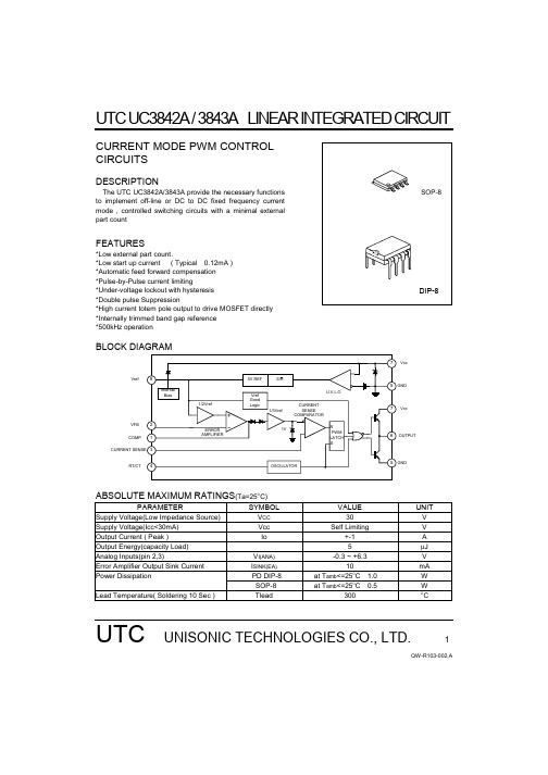
UTC UC3842A / 3843A LINEAR INTEGRATED CIRCUITUTC UNISONIC TECHNOLOGIES CO., LTD.1QW-R103-002,ACURRENT MODE PWM CONTROL CIRCUITSDESCRIPTIONThe UTC UC3842A/3843A provide the necessary functions to implement off-line or DC to DC fixed frequency current mode , controlled switching circuits with a minimal external part countFEATURES*Low external part count. *Low start up current ( Typical 0.12mA ) *Automatic feed forward compensation *Pulse-by-Pulse current limiting*Under-voltage lockout with hysteresis *Double pulse Suppression*High current totem pole output to drive MOSFET directly *Internally trimmed band gap reference *500kHz operationBLOCK DIAGRAMVref VFB COMPRT/CT VccOUTPUTVccABSOLUTE MAXIMUM RATINGS (Ta=25°C)PARAMETER SYMBOL VALUE UNITSupply Voltage(Low Impedance Source) V CC 30 VSupply Voltage(Icc<30mA) Vcc Self Limiting V Output Current ( Peak ) Io +-1 AOutput Energy(capacity Load) 5µJ Analog Inputs(pin 2,3) V I(ANA) -0.3 ~ +6.3 V Error Amplifier Output Sink Current I SINK(EA) 10 mAPower Dissipation PD DIP-8 at T amb <=25°C 1.0 W SOP-8 at T amb <=25°C 0.5 WLead Temperature( Soldering 10 Sec ) Tlead 300 °CUTC UC3842A / 3843A LINEAR INTEGRATED CIRCUITUTC UNISONIC TECHNOLOGIES CO., LTD.2QW-R103-002,A(continued)PARAMETRER SYMBOL VALUE UNITStorage Temperature Tstg -65 ~ +150°C Note 1: Ta>25°C, P D derated with 8mW/°C.ELECTRICAL CHARACTERISTICS (0°C <=Ta<=70°C,V CC =15V,R T =10k Ω,C T =3.3nF,unless otherwise specified)PARAMETER SYMBOL TEST CONDITIONS MIN TYP MAX UNITReference SectionOutput Voltage V REF Tj=25°C,Io=1mA 4.9 5 5.1 V Line Regulation ∆V REF 12<=V IN <=25V 6 20 mV Load Regulation ∆V REF1<=Io =20mA 6 25 mV Temperature Stability (Note 2) 0.2 0.4 mV/°CTotal Output Variation Line, Load, Temp(note 2) 4.82 5.18 V Output Noise Voltage Vosc 10Hz<=f<=10kHz,Tj=25°C (note 2) 50 uVLong Term Stability Ta=25°C,1000Hrs(note 2) 5 25 mV Output Short Circuit I SC -30-100 -180 mAOscillator Section Initial Accuracy f Tj=25°C 47 52 57 kHz Voltage Stability ∆f/∆Vcc 12<=Vcc<=25V 0.2 1 % Temperature Stability Tmin<=T A <=Tmax(note 2) 5 % Amplitude Vosc Vpin 4 peak to peak 1.7 VError Amplifier SectionInput Voltage V I(EA) Vpin 1=2.5V 2.42 2.50 2.58 V Input Bias Current I BIAS -0.3 -2 µA A VOL 2 <=Vo<=4V 60 90 dB Unity Gain Bandwidth Tj=25°C (note 2) 0.7 1 MHz PSRR I2<=Vcc<=25V 60 70 dB Output Sink Current Isink Vpin 2=2.7V,Vpin 1=1.1V 2 6 mA Output Source Current Isource Vpin 2=2.3V,Vpin 1=5V -0.5-0.8 mA Vout High V OH Vpin 2=2.3V, RL=15k Ω to GND 5 6 V Vout Low V OL Vpin 2=2.7V,Vpin 1=1.1V 0.7 1.1 VCurrent Sense sectionGain G V (note 3,4) 2.85 3 3.15 V/V Maximum Input signal V I(MAX)Vpin 1=5V( note 3) 0.9 1 1.1 V PSRR 12<=Vcc<=25V 70 dB Input Bias Current I BIAS -2 -10 µA Delay to Output Vpin 3=0 to 2V 150 300 nsOutput SectionOutput Low Level V OL Isink =20mA 0.1 0.4 VIsink =200mA 1.5 2.2 V Output High Level V OH Isource =20mA 13 13.5 V Isource =200mA 12 13.5 VRise Time t R Tj=25°C,C L =1nF(note 2)50 150 ns Fall Time t F Tj=25°C,C L =1nF(note 2)50 150 ns Under-Voltage Lockout Output SectionStart Threshold V TH(ST)UTC3842A 14.516 17.5 V UTC3843A 7.88.4 9 V Min. Operating Voltage V OPR(min)After Turn On UTC3842A8.510 11.5UTC3843A 7 7.6 8.2 VPWM SectionMaximum Duty Cycle D (MAX) 95 97 100 %UTC UC3842A / 3843A LINEAR INTEGRATED CIRCUITUTC UNISONIC TECHNOLOGIES CO., LTD.3QW-R103-002,APARAMETER SYMBOLTEST CONDITIONS MINTYP MAX UNITMinimum Duty CycleD (MIN)0 % Total Standby CurrentStart-up Current I ST 0.12 0.3 mAOperating Supply Current I CC(opr)Vpin 2=Vpin 3=0V 11 17 mA Vcc Zener Voltage Vz Icc=25mA 34 V note 2:These parameters, although guaranteed ,are not 100% tested in production. note 3:Parameters measured at trip point of latch with Vpin 2=0. note 4:Gain defined as:∆Vpin 1∆Vpin 3A=; 0<=Vpin3<=0.8Vnote 5:Adjust Vcc above the start threshold before setting at 15V.OPEN-LOOP LABORATORY TEST FIXTUREVrefVccAdjustHigh peak current associated with capacity loads necessitate careful grounding techniques. Timing and bypass capacitors should be connected close to pin 5 in single point GND. The transistor and 5k Ω potentio-meter are used to sample the oscillator waveform and apply an adjustable Ramp to Pin 3.UNDER-VOLTAGE LOCKOUTVonVoffVccDuring Under-Voltage Lockout, the output driver is biased to a high impedance state. Pin 6 should be shunt to GND with a bleeder resistor to prevent activating the power switch with output leakage currents.UTC UC3842A / 3843A LINEAR INTEGRATED CIRCUITUTC UNISONIC TECHNOLOGIES CO. LTD4QW-R103-002,AERROR AMPLIFIER CONFIGURATIONError amplifier can source or sink up to 0.5mACURRENT SENSE CIRCUITPeak current (Is) determined by the formula:Ismax=10V/Rs.A small RC filter be required to suppress switch transients.SLOPE COMPENSATIONA fraction of the oscillator ramp can be resistively summed with the current sense signal to provide slopecompensation for converts requiring duty cycles over 50%.Note that capacitor C, forms a filter with R2 to suppress the leading edge switch spikes.UTC UC3842A / 3843A LINEAR INTEGRATED CIRCUITUTC UNISONIC TECHNOLOGIES CO. LTD5QW-R103-002,AOSCILLATOR SECTIONLarge RT Small CTSmall RT Large CTV4V4INTERNAL CLOCKINTERNAL CLOCKDead time VS C T (R T >5k Ω) TimingResistance Vs Frequency 1101001101000.1td (µs)CT (nF)110RT (k ΩFrequency (Hz)SHUTDOWN TECHNIQUESShutdown UTC UC3842A can be accomplished by two methods; either raise pin 3 above 1V or pull Pin 1 below a voltage two diode drops above ground. Either method caused the output of PWM comparator to be high(refer to block diagram).The PWM latch is reset dominant so that the output will remain low until the next clock cycle after the shutdown condition at pins 1 and/or 3 is removed . In one example, an externally latched shut –down may be accomplished by adding an SCR which be reset by cycling Vcc below the lower UVLO threshold. At this point the reference turns off allowing the SCR to reset.UTC UC3842A / 3843A LINEAR INTEGRATED CIRCUITUTC UNISONIC TECHNOLOGIES CO. LTD6QW-R103-002,ATYPICAL PERFORMANCE CHARACTERISTICS0.010.1101234S a t u r a t i o n V o l t a g e (V )Output Current(Sourse or Sink Current) (A)7103106105104101021020406010080Frequency (Hz)V o l t a g e G a i n (d B )-180-135-90-45P H A S E (D e g r e e )Output Saturation Characteristics Error Amplifier Open-Loop Frequency ResponseUTC UC3842A / 3843A LINEAR INTEGRATED CIRCUITUTC UNISONIC TECHNOLOGIES CO. LTD7QW-R103-002,A-50-25255075100125150Vref (V)Temperature (°C)-50-250255075100125150I s t a r t (m A )Temperature (°C)-50-252550751001251509101112131415Icc (mA)Temperature (°C)Vref Temperature DriftIstart Temperature DriftIcc Temperature Drift。
UC3844中文资料

UC3844,UC3845中文资料UC3844 UC3845 是高性能固定频率电流模式控制器专为离线和直流至直流变换器应用而设计,为设计人员提供只需最少外部元件就能获得成本效益高的解决方案。
这些集成电路具有可微调的振荡器、能进行精确的占空比控制、温度补偿的参考、高增益误差放大器。
电流取样比较器和大电流图腾柱式输出,是驱动功率MOSFET的理想器件。
其它的保护特性包括输入和参考欠压锁定,各有滞后、逐周电流限制、可编程输出静区时间和单个脉冲测量锁存。
这些器件可提供8脚双列直插塑料封装和14脚塑料表面贴装封装(SO-14)。
SO-14封装的图腾柱式输出级有单独的电源和接地管脚。
UC3844 有16V(通)和10 伏(断)低压锁定门限,十分适合于离线变换器。
UC3845是专为低压应用设计的,低压锁定门限为8.5伏(通)和7.6V(断)。
UC3844,UC3845特点:自动前馈补偿锁存脉宽调制,可逐周限流内部微调的参考电压,带欠压锁定大电流图腾柱输出欠压锁定,带滞后低启动和工作电流直接与安森美半导体的SENSEFET产品接口电流模式工作到500KHZ输出静区时间从50%到70%可调UC3844 的振荡工作频率由引脚4 与引脚8 之间所接定时电阻RT、脚4 与地之间所接定时电容CT 设定。
计算公式为: f = 1/T = RTCT/0.55 = 1.72RTCT。
引脚2 是电压反馈端,将取样电压加至E/A 误差放大器的反相输入端,与同向输入端的2.5 V 基准电压进行比较,产生误差电压。
利用内部E/A 误差放大器可以构成电压环。
引脚3 是电流反馈端,电流取样电压由引脚3 输入到电流比较器。
当引脚3 电压大于1V 时,输出关闭。
利用引脚3 和电流比较器可以构成电流环。
引脚1 是补偿端,外接阻容元件以补偿误差放大器的频率特性。
引脚8 为5V 基准电压,带载能力50mA。
引脚6 为推挽输出端,有拉、灌电流的能力。
UC3843数据手册_引脚图_参数

Page
• Added Applications section, Device Information table, Pin Configuration and Functions section, Specifications section, Detailed Description section, Application and Implementation section, Power Supply Recommendations section, Layout section, Device and Documentation Support section, and Mechanical, Packaging, and Orderable Information section ................................................................................................................................................................. 1
4 Revision History
NOTE: Page numbers for previous revisions may differ from page numbers in the current version.
Changes from Revision D (July 2011) to Revision E
7.1 Absolute Maximum Ratings ...................................... 5 7.2 ESD Ratings.............................................................. 5 7.3 Recommended Operating Conditions....................... 5 7.4 Thermal Information .................................................. 6 7.5 Electrical Characteristics........................................... 6 7.6 Typical Characteristics .............................................. 8 8 Detailed Description .............................................. 9 8.1 Overview ................................................................... 9 8.2 Functional Block Diagram ......................................... 9 8.3 Feature Description................................................... 9 8.4 Device Functional Modes........................................ 12
UC3843开关电源
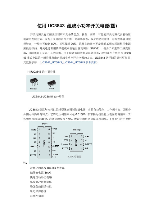
使用UC3843 组成小功率开关电源(图)开关电源具有工频变压器所不具备的优点,新型、高效、节能的开关电源代表着稳压电源的发展方向,因为开关电源内部工作于高频率状态,本身的功耗很低,电源效率就可做得较高,一般均可做到80%,甚至接近90%。
这样高的效率不是普通工频变压器稳压电源所能比拟的。
开关电源常用的单端或双端输出脉宽调制(PWM),省去了笨重的工频变压器,可制成几瓦至几千瓦的电源。
用于脉宽调制的集成电路很多,我们现在介绍的是UC38 43集成电路的一般特性及由它组成小功率开关电源的方法。
UC3843更详细的资料可参见其数据手册。
(UC3842_UC3843_UC3844_UC3845参考资料)[1].UC3843的主要特性UC3842-UC3845的外形图UC3843是近年来问世的新型脉宽调制集成电路,它具有功能全,工作频率高,引脚少外围元件简单等特点,它的电压调整率可达0.01%V,非常接近线性稳压电源的调整率。
工作频率可达500kHz,启动电流仅需1mA,所以它的启动电路非常简单。
下面是它的主要特性:最优化的离线DC-DC变换器低静态电流(1mA)快速自动补偿电路单步脉冲控制电路增强负载回馈特性断电停滞特性双脉冲抑制大电流标识输出内置能隙参考电压500kHz的工作频率低Ro过零放大器[2].UC3843的工作原理UC3843有4种封装形式,一种是14pin双列直插和SOP-14,另一种是8pin双列直插和SOP-8。
我们以最简的8pin封装简述其工作原理。
[IMG]20072289575883293.gif[/IM G] pin(1)是补偿端,外接电阻电容元件以补偿误差放大器的频率特性。
第(2)脚是反馈端,将取样电压加至误差放大器的反相输入端,再与同相输入端的基准电压进行比较,输出误差控制电压。
第(3)脚接过流检测电阻,组成过流保护电路。
RT/RC为锯齿波振荡器的定时电阻和电容的公共端,内部基准电压为VREF=5V。
- 1、下载文档前请自行甄别文档内容的完整性,平台不提供额外的编辑、内容补充、找答案等附加服务。
- 2、"仅部分预览"的文档,不可在线预览部分如存在完整性等问题,可反馈申请退款(可完整预览的文档不适用该条件!)。
- 3、如文档侵犯您的权益,请联系客服反馈,我们会尽快为您处理(人工客服工作时间:9:00-18:30)。
TJ = 25°C TA = Tlow to Thigh Frequency Change with Voltage (VCC = 12 V to 25 V) Frequency Change with Temperature TA = Tlow to Thigh
Vref Undervoltage
Lockout
Oscillator
+ − Error Amplifier
Latching PWM
GND 5(9) Pin numbers in parenthesis are for the D suffix SOIC−14 package.
VC
7(11) Output
These devices are available in an 8−pin dual−in−line plastic package as well as the 14−pin plastic surface mount (SOIC−14). The SOIC−14 package has separate power and ground pins for the totem pole output stage.
Operating Junction Temperature
Operating Ambient Temperature UC3842A, UC3843A UC2842A, UC2843A
Vin
− 0.3 to + 5.5 V
IO
10
mA
PD RqJA
PD RqJA
TJ TA
862 145
1.25 100 + 150
47
−
60
46
0.2
1.0
−
5.0
−
−
5.0
5.1
2.0
20
3.0
25
0.2
−
−
5.18
50
−
5.0
−
− 85 − 180
52
57
−
60
0.2
1.0
5.0
−
Oscillator Voltage Swing (Peak−to−Peak)
Discharge Current (Vosc = 2.0 V) TJ = 25°C TA = Tlow to Thigh
Also included are protective features consisting of input and reference undervoltage lockouts each with hysteresis, cycle−by−cycle current limiting, programmable output deadtime, and a latch for single pulse metering.
Current Sense 3 RT/CT 4
8 Vref 7 VCC 6 Output 5 GND
(Top View)
Compensation 1 NC 2
Voltage Feedback 3 NC 4
Current Sense 5 NC 6
RT/CT 7
14 Vref 13 NC 12 VCC 11 VC 10 Output 9 GND 8 Power Ground
UC3842A, UC3843A, UC2842A, UC2843A
High Performance Current Mode Controllers
The UC3842A, UC3843A series of high performance fixed frequency current mode controllers are specifically designed for off−line and DC−to−DC converter applications offering the designer a cost effective solution with minimal external components. These integrated circuits feature a trimmed oscillator for precise duty cycle control, a temperature compensated reference, high gain error amplifier, current sensing comparator, and a high current totem pole output ideally suited for driving a power MOSFET.
0 to + 70 − 25 to + 85
mW °C/W
W °C/W
°C °C
Storage Temperature Range
Tstg
− 65 to + 150 °C
Maximum ratings are those values beyond which device damage can occur. Maximum ratings applied to the device are individual stress limit values (not normal operating conditions) and are not valid simultaneously. If these limits are exceeded, device functional operation is not implied, damage may occur and reliability may be affected.
8 1
14 1
PDIP−8 N SUFFIX CASE 626
SOIC−14 D SUFFIX CASE 751A
8 1
SOIC−8 D1 SUFFIX Cቤተ መጻሕፍቲ ባይዱSE 751
PIN CONNECTIONS
Compensation 1 Voltage Feedback 2
(Top View)
© Semiconductor Components Industries, LLC, 2005
November, 2005 − Rev. 8
ORDERING INFORMATION
See detailed ordering and shipping information in the package dimensions section on page 15 of this data sheet.
UC284XA
UC384XA
Characteristics
Symbol Min
Typ
Max Min
Typ
Max
REFERENCE SECTION Reference Output Voltage (IO = 1.0 mA, TJ = 25°C) Line Regulation (VCC = 12 V to 25 V) Load Regulation (IO = 1.0 mA to 20 mA) Temperature Stability
6(10) Power Ground
5(8)
Current Sense 3(5) Input
Figure 1. Simplified Block Diagram
MAXIMUM RATINGS
Rating
Symbol
Value
Unit
Bias and Driver Voltages (Zero Series Impedance, see also Total Device spec) Total Power Supply and Zener Current Output Current, Source or Sink (Note 1) Output Energy (Capacitive Load per Cycle)
Vref Regline Regload
TS Vref Vn
S ISC
fosc
Dfosc/DV Dfosc/DT
4.95 − − − 4.9 −
− − 30
47 46 − −
5.0
5.05
4.9
2.0
20
−
3.0
25
−
0.2
−
−
−
5.1
4.82
50
−
−
5.0
−
−
− 85 − 180 − 30
52
57
The UCX842A has UYLO thresholds of 16 V (on) and 10 V (off), ideally suited for off−line converters. The UCX843A is tailored for lower voltage applications having UVLO thresholds of 8.5 V (on) and 7.6 V (off).
Total Output Variation over Line, Load, Temperature
Output Noise Voltage (f = 10 Hz to 10 kHz, TJ = 25°C) Long Term Stability (TA = 125°C for 1000 Hours) Output Short Circuit Current
VCC, VC
30
V
(ICC + IZ)
30
mA
IO
1.0
A
W
5.0