bq76PL536:电池管理集成电路
Injoinic IP5306 全集成电源管理芯片说明书

Fully-Integrated Power Bank System-On-Chip with2.1A charger, 2.4A dischargerFeatures•Switch buck charger and boost✧ 2.1A Synchronous switching charger and 5V2.4A boost converter✧Boost converter efficiency up to 92%✧Switching charger efficiency up to 91%✧Integrated power-path management,charging batteries and charging cellphonesat the same time•Charger✧Adaptive charging current control, excellentadapter compatibility✧Support 4.20/4.30/4.35/4.40V batteries •State of charge (SOC) indicator✧Integrated LED controller supports 4/3/2/1LEDs as the SOC indicator•Fully featured✧Key ON/OFF✧Integrated flashlight controller✧Integrated cellphone plug-in and plug-outdetector•Low power✧Smart load detector, switching to standbymode automatically✧<100 µA standby current•Ultra simplified BOM✧Integrated power FET, charging/boostingwith a single inductor•Multiple protections, high reliability✧Output over-current, over-voltage,short-circuit protection✧Input over-voltage, over-current, batteryover-charge, over-drain, over-currentprotection✧Thermal Shutdown✧ESD 4KVApplications•Power bank, Portable Charger•Mobile Phones, Smart Phones, Handheld Devices, Portable Media Player, TabletDescriptionIP5306 is a fully-integrated multi-function power management SoC. It integrates a boost converter, a Li battery charger management system and a battery state of charge indicate controller. It provides a turn-key solution for power bank and portable charger applications.IP5306’s high integration and rich features make the minimized component number in application. It can effectively downsize the application and lower the BOM cost.IP5306 only needs a single inductor to realize step-down and step-up which provides 2.4A output current.It can switch to standby mode at light load automaticallyIP5306’s synchronous s witching charger provides 2A charging current. Its efficiency is up to 91%. It regulates the charging current by IC temperature and input voltage.。
多节电池解决方案
3S~5S
6S~10S
9S~15S
16S
主动保护与电 主动保护与电 主动保护与电 主动保护与电
池平衡
池平衡
池平衡
池平衡
包含全面的保護 : OV, UV, OCD, SCD, OCC, OT-D, OT-C, UT. 低端 N-Mosfet , SMBus 通訊協定並且可讀取電池電壓、溫度、
電流。 支援黑盒子記錄功能。
• 20-pin SSOP
Notes: OV=过压, UV=欠压, OT=过温, SC=短路,OP=电池掉电检测, OCD=放电过电流, OCC=充电过电流, IT=阻抗追踪技术
Monitoring – Balancing – Protecting (2 /3 page )
bq77920
AFE FET Drive
,CS_N/S线的正常操作在通信期间即被置为有效状态(逻辑高电平),而堆栈中适 当的bq76PL536A将根据作为分组的一部分进行传输的地址做出响应。 当bq76PL536A复位时,DEVICE_STATUS[AR](地址请求)标记被清零,地址寄 存器被设定为0x00,且ALERT_S被置位并沿堆栈向下传递。 。在该状态中(地址 = 0x00),CS_N信号被强制为一种“解除有效”的状态(当 一个地址 = 0时,CS不向北传递)。这样,在一个复位之后,主机确信:在地址 0x00处的一个响应来自堆栈中的第一个物理器件。在当前器件的地址分配之后,主机 确信:地址0x00处的下一个响应来自堆栈中的下一个物理器件。 当给器件分配了一个有效地址后,CS_N信号正常做出响应,并跟随CS_H或CS_S信 号传播至堆栈中的下一个器件。 有效地址处于0x01至0x3e的范围内。0x00专留作复位之后的器件发现之用。0x3f 则专留作所有器件的一个广播地址。
XB5352G 贴片SOT23-5 单节锂电池充电保护芯片 电源管理IC
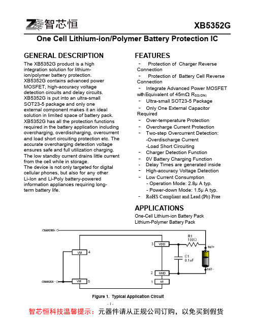
XB5352G ____________________________________________________________________________________________________________________________ One Cell Lithium-ion/Polymer Battery Protection ICGENERAL DESCRIPTIONThe XB5352G product is a high integration solution for lithium-ion/polymer battery protection.XB5352G contains advanced power MOSFET, high-accuracy voltage detection circuits and delay circuits.XB5352G is put into an ultra-smallSOT23-5 package and only oneexternal component makes it an ideal solution in limited space of battery pack. XB5352G has all the protection functions required in the battery application including overcharging, overdischarging, overcurrent and load short circuiting protection etc. The accurate overcharging detection voltage ensures safe and full utilization charging. The low standby current drains little current from the cell while in storage.The device is not only targeted for digital cellular phones, but also for any otherLi-Ion and Li-Poly battery-powered information appliances requiring long-term battery life. FEATURES·Protection of Charger Reverse Connection·Protection of Battery Cell Reverse Connection·Integrate Advanced Power MOSFET with Equivalent of 45mΩ R SS(ON)·Ultra-small SOT23-5 Package ·Only One External Capacitor Required·Over-temperature Protection ·Overcharge Current Protection ·Two-step Overcurrent Detection: -Overdischarge Current-Load Short Circuiting·Charger Detection Function·0V Battery Charging Function- Delay Times are generated inside ·High-accuracy Voltage Detection ·Low Current Consumption- Operation Mode: 2.8μA typ.- Power-down Mode: 1.5μA typ. ·RoHS Compliant and Lead (Pb) FreeAPPLICATIONSOne-Cell Lithium-ion Battery PackLithium-Polymer Battery PackFigure 1. Typical Application CircuitORDERING INFORMATIONNote: “YW” is manufacture date code, “Y” means the year, “W” means the weekPIN CONFIGURATIONFigure 2. PIN ConfigurationPIN DESCRIPTIONABSOLUTE MAXIMUM RATINGS(Note: Do not exceed these limits to prevent damage to the device. Exposure to absolute maximum rating conditions for long periods may affect device reliability.)ELECTRICAL CHARACTERISTICSTypicals and limits appearing in normal type apply for T A= 25o C, unless otherwise specifiedFigure 3. Functional Block Diagram FUNCTIONAL DESCRIPTIONThe XB5352G monitors the voltage and current of a battery and protects it from being damaged due to overcharge voltage, overdischarge voltage, overdischarge current, and short circuit conditions by disconnecting the battery from the load or charger. These functions are required in order to operate the battery cell within specified limits.The device requires only one external capacitor. The MOSFET is integrated andits R SS(ON) is as low as45mΩtypical. Normal operating modeIf no exception condition is detected, charging and discharging can be carried out freely. This condition is called the normal operating mode.Overcharge ConditionWhen the battery voltage becomes higher than the overcharge detection voltage (V CU) during charging under normal conditionand the state continues for the overcharge detection delay time (t CU) or longer, theXB5352G turns the charging control FEToff to stop charging. This condition is called the overcharge condition. The overcharge condition is released in the following two cases:1, When the battery voltage drops below the overcharge release voltage (V CL), the XB5352G turns the charging control FET on and returns to the normal condition.2, When a load is connected and discharging starts, the XB5352G turns the charging control FET on and returns to the normal condition. The release mechanism is as follows: the discharging current flows through an internal parasitic diode of the charging FET immediately after a load is connected and discharging starts, and the VM pin voltage increases about 0.7 V (forward voltage of the diode) from the GND pin voltage momentarily. TheXB5352G detects this voltage and releases the overcharge condition. Consequently, in the case that the battery voltage is equal to or lower than the overcharge detection voltage (V CU), the XB5352G returns to the normal condition immediately, but in the case the battery voltage is higher than the overcharge detection voltage (V CU),the chip does not return to the normal condition until the battery voltage drops below the overcharge detection voltage (V CU) even if the load is connected. In addition, if the VM pin voltage is equal to or lower than the overcurrent 1 detection voltage when a load is connected and discharging starts, the chip does not return to the normal condition.Remark If the battery is charged to a voltage higher than the overcharge detection voltage (V CU) and the battery voltage does not drops below the overcharge detection voltage (V CU) even when a heavy load, which causes an overcurrent, is connected, the overcurrent 1 and overcurrent 2 do not work until the battery voltage drops below the overcharge detection voltage (V CU). Since an actual battery has, however, an internal impedance of several dozens of mΩ, and the battery voltage drops immediately after a heavy load which causes an overcurrent is connected, the overcurrent 1 and overcurrent 2 work. Detection of load short-circuiting works regardless of the battery voltage.Overdischarge ConditionWhen the battery voltage drops below the overdischarge detection voltage (V DL) during discharging under normal condition and it continues for the overdischarge detection delay time (t DL) or longer, theXB5352G turns the discharging control FET off and stops discharging. This condition is called overdischarge condition. After the discharging control FET is turned off, the VM pin is pulled up by the R VMD resistorbetween VM and VDD in XB5352G. Meanwhile when VM is bigger than 1.5V (typ.) (the load short-circuiting detection voltage), the current of the chip is reduced to the power-down current (I PDN). This condition is called power-down condition. The VM and VDD pins are shorted by theR VMD resistor in the IC under the overdischarge and power-down conditions. The power-down condition is released when a charger is connected and the potential difference between VM and VDD becomes 1.3 V (typ.) or higher (load short-circuiting detection voltage). At this time, the FET is still off. When the battery voltage becomes the overdischarge detection voltage (V DL) or higher (see note), the XB5352G turns the FET on and changes to the normal condition from the overdischarge condition.Remark If the VM pin voltage is no less than the charger detection voltage (V CHA), when the battery under overdischarge condition is connected to a charger, the overdischarge condition is released (the discharging control FET is turned on) as usual, provided that the battery voltage reaches the overdischarge release voltage (V DU) or higher. Overcurrent ConditionWhen the discharging current becomes equal to or higher than a specified value (the VM pin voltage is equal to or higher than the overcurrent detection voltage)during discharging under normal condition and the state continues for the overcurrent detection delay time or longer, theXB5352G turns off the discharging control FET to stop discharging. This condition is called overcurrent condition. (The overcurrentincludes overcurrent, or load short-circuiting.)The VM and GND pins are shorted internally by the R VMS resistor under the overcurrent condition. When a load is connected, the VM pin voltage equals the VDD voltage due to the load.The overcurrent condition returns to the normal condition when the load is released and the impedance between the B+ and B- pins becomes higher than the automatic recoverable impedance. When the load is removed, the VM pin goes back to the GND potential since the VM pin is shorted the GND pin with the R VMS resistor. Detecting that the VM pin potential is lower than the overcurrent detection voltage(V IOV), the IC returns to the normal condition.Abnormal Charge Current DetectionIf the VM pin voltage drops below the charger detection voltage (V CHA) during charging under the normal condition and it continues for the overcharge detection delay time (t CU) or longer, the XB5352G turns the charging control FET off and stops charging. This action is called abnormal charge current detection. Abnormal charge current detection works when the discharging control FET is on and the VM pin voltage drops below the charger detection voltage (V CHA). When an abnormal charge current flows into a battery in the overdischarge condition, the XB5352G consequently turns the charging control FET off and stops charging after the battery voltage becomes the overdischarge detection voltage and the overcharge detection delay time (t CU) elapses.Abnormal charge current detection is released when the voltage difference between VM pin and GND pin becomes lower than the charger detection voltage (V CHA) by separating the charger. Since the 0 V battery charging function has higher priority than the abnormal charge current detection function, abnormal charge current may not be detected by the product with the 0 V battery charging function while the battery voltage is low.Load Short-circuiting conditionIf voltage of VM pin is equal or below short circuiting protection voltage (V SHORT), the XB5352G will stop discharging and battery is disconnected from load. The maximum delay time to switch current off is t SHORT. This status is released when voltage of VM pin is higher than short protection voltage (V SHORT), such as when disconnecting the load.Delay CircuitsThe detection delay time for overdischarge current 2 and load short-circuiting starts when overdischarge current 1 is detected. As soon as overdischarge current 2 or load short-circuiting is detected over detection delay time for overdischarge current 2 or load short- circuiting, the XB5352G stops discharging. When battery voltage falls below overdischarge detection voltage due to overdischarge current, the XB5352G stop discharging by overdischarge current detection. In this case the recovery of battery voltage is so slow that if battery voltage after overdischarge voltage detection delay time is still lower than overdischarge detection voltage, the XB5352G shifts to power-down.Figure 4. Overcurrent delay time0V Battery Charging Function (1) (2) (3) This function enables the charging of a connected battery whose voltage is 0 V by self-discharge. When a charger having 0 V battery start charging charger voltage(V0CHA) or higher is connected between B+ and B- pins, the charging control FET gate is fixed to VDD potential. When the voltage between the gate and the source of the charging control FET becomes equal to or higher than the turn-on voltage by the charger voltage, the charging control FET is turned on to start charging. At this time, the discharging control FET is off and the charging current flows through the internal parasitic diode in the discharging control FET. If the battery voltage becomes equal to or higher than the overdischarge release voltage (V DU), the normal condition returns. Note(1) Some battery providers do not recommend charging of completely discharged batteries. Please refer to battery providers before the selection of 0 V battery charging function.(2) The 0V battery charging function has higher priority than the abnormal charge current detection function. Consequently, a product with the 0 V battery charging function charges a battery and abnormal charge current cannot be detected during the battery voltage is low (at most 1.8 V or lower).(3) When a battery is connected to the IC for the first time, the IC may not enter the normal condition in which discharging is possible. In this case, set the VM pin voltage equal to the GND voltage (short the VM and GND pins or connect a charger) to enter the normal condition.TIMING CHART1.Overcharge and overdischarge detectionV V CU -V V DL +V V DL ONONCHARGEV DDV ov1V SS V VMFigure5-1 Overcharge and Overdischarge Voltage Detection2.Overdischarge current detectionV CU V CU -V HC V DL +V DH V DLONDISCHARGEOFFV DDV V ov2V ov1V SS(1)(4)(1)(1)(1)(4)(4)Figure5-2 Overdischarge Current DetectionRemark: (1) Normal condition (2) Overcharge voltage condition (3) Overdischarge voltage condition (4)Overcurrent condition3.Charger DetectionVV CU-VV DL+VV DLONV DDVMV SSVFigure5-3 Charger Detection4.Abnormal Charger DetectionVV CU-VV DL+VV DLONONCHARGEV DDVMV SSVFigure5-4 Abnormal Charger DetectionRemark: (1) Normal condition (2) Overcharge voltage condition (3) Overdischarge voltage condition (4)Overcurrent conditionTYPICAL CHARACTERISTICS(Test based on XB5352G version, V BAT = 3.6V, T A= 25 C unless otherwise specified)Internal FET On-Resistance vs. Junction TemperatureTYPICAL APPLICATIONAs shown in Figure 6, the bold line is the high density current path which must be kept as short as possible. For thermal management, ensure that these trace widths are adequate. C1 is a decoupling capacitor which should be placed as close as possible to XB5352G.Fig 6 XB5352G in a Typical Battery Protection CircuitPrecautions• Pay attention to the operating conditions for input/output voltage and load current so that the power loss in XB5352G does not exceed the power dissipation of the package.• Do not apply an el ectrostatic discharge to this XB5352G that exceeds the performance ratings of the built-in electrostatic protection circuit.XB5352G______________________________________ ____________________________________________________ ________ _________ ____________ - 11 -PACKAGE OUTLINESOT23-5 PACKAGE OUTLINE AND DIMENSIONS。
锂电池转1.5v专用充放电管理芯片
锂电池转1.5v专用充放电管理芯片1.引言概述部分的内容可以如下编写:1.1 概述随着现代电子产品的普及和多样化,锂电池作为一种理想的能源储备方式,得到了越来越广泛的应用。
然而,在许多消费电子设备中,如遥控器、手电筒等,依然需要使用1.5V电压的电池。
为了满足这些设备的需求,开发一种能够将锂电池的高电压转换为1.5V的专用充放电管理芯片变得非常重要。
本文将重点介绍一种专门设计用于锂电池转换为1.5V电压的充放电管理芯片。
通过这种管理芯片,用户可以更灵活地使用锂电池,以满足各种设备的能源需求。
同时,该管理芯片还能提供电池状态监测、充电保护等功能,增强了锂电池的安全性和可靠性。
在本文中,我们将详细介绍锂电池的特点以及1.5V专用充放电管理芯片的需求。
探讨锂电池的优势,讨论转换为1.5V电压对于电子设备的意义。
我们还将探讨该管理芯片的发展前景和应用前景,展望未来锂电池管理技术的发展方向。
通过本文的阐述,读者将能够了解到锂电池转换1.5V专用充放电管理芯片的重要性和优势,以及该技术的应用前景。
同时,读者也可以通过本文对相关技术的介绍,进一步了解锂电池的特点和在电子设备中的应用。
接下来的章节将逐一介绍锂电池的特点以及1.5V专用充放电管理芯片的需求,帮助读者全面了解该技术的背景和应用场景。
文章结构部分的内容可以如下编写:1.2 文章结构本文将围绕锂电池转1.5V专用充放电管理芯片展开讨论,共分为引言、正文和结论三个部分。
引言部分(Chapter 1)首先概述了本文的研究背景和目的,介绍了锂电池和1.5V专用充放电管理芯片的基本情况,并提出了文章的研究动机。
正文部分(Chapter 2)主要分为两个小节。
首先(Section 2.1),我们将详细探讨锂电池的特点,包括其优点和缺点,以及当前在各个领域的广泛应用。
其次(Section 2.2),我们将深入分析1.5V专用充放电管理芯片的需求,包括其功能和特性,以及应用领域和市场需求。
AD536(CN)(中文需参看英文图表)

RMS to DC转换AD536A功能:有效值到直流电平装换高精度激光微调技术0.2%最大误差(AD536AX)0.5%最大误差(AD536AJ)宽响应能力:能够计算AC和DC信号的RMS450KHz带宽:Vrms>100mV2MHz带宽:Vrms>1V信号的波峰因数当误差为1%时为7dB输出有60dB范围低功耗:1.2mA静态电流单、双端均可用整体集成电路-55℃ to 125℃(AD536AS)产品描述AD536A是一款RMS到直流转换的整体集成电路,它优于混合式或组合式的电路。
AD536A直接计算输入波形的RMS值,包括AC和DC组件。
有一个波峰因数补偿表,可以使波峰系数达到7的测量值只有1%的误差。
本器件能测量300K 带宽大于100mV的信号,误差在3dB范围内。
AD536A有一项重要的新功能,能够将rms电平转换成dB值输出。
信号rms的对数输出到独立的管脚进行dB转换,其范围有60dB。
利用一个外部的参考电流,用户能够很方便地设置0dB电平,能计算输入的任何0.1到2Vrms波形。
AD536A在晶圆级采用激光校准对输入输出补偿,正负波形平衡,7Vrms满量程精度。
因此,无需外部调整,即可达到额定精度。
输入输出均有完全保护,输入电平可超出供电电平。
输入连接失去供电不会损坏芯片。
输出有短路保护。
AD536A商用产品分两个精度级别(A,K)温度范围(0℃ to 70℃)和另一个超范围级别(S)温度范围-55℃ to 125℃。
AD536AK有最大±2mV±0.2%的读取误差,而AD536AJ和AD536AS有±5mV±0.5%的最大误差。
所有三种都可用14-DIP 或10to100脚金属封装。
AD536AS也有20脚无铅陶瓷封装。
产品特点1、AD536A计算输入的复合AC信号输出等效直流电平。
计算信号的rms值比信号电平均值更有用,因为rms反映了信号的功率,还反映了信号的标准偏差。
电源管理芯片目录大全
电源管理芯片目录大全1.高效3A开关稳压器AP15012.低噪声电荷泵DC-DC电源转换器AAT31143.高性能降压式DC-DC电源转换器ISL64204.高效率DC-DC电源转换控制器IRU30375.小功率极性反转电源转换器ICL76606.单片降压式开关稳压器L49607.1A高效率升压/降压式DC-DC电源转换器L59708.2A高效率单片开关稳压器L49789.大功率开关稳压器L4970A10.1.5A降压式开关稳压器L497111.高效率5A开关稳压器LM267812.3A降压开关稳压器LM259613.高效率1A降压单片开关稳压器LM1575/LM2575/LM2575HV14.3A降压单片开关稳压器LM2576/LM2576HV15.可调升压开关稳压器LM257716.低噪声升压式电源转换器LM275017.电流模式升压式电源转换器LM273318.小型75V降压式稳压器LM500719.升压式DC-DC电源转换器LM2703/LM270420.电流模式升压式电源转换器LM273321.低功耗升/降压式DC-DC电源转换器LT107322.升压式DC-DC电源转换器LT161523.隔离式开关稳压器LT172524.大电流高频降压式DC-DC电源转换器LT176525.低噪声高效率降压式电荷泵LTC191126.大电流升压转换器LT193527.高效升压式电荷泵LT193728.低噪声电荷泵LTC320029.微型低功耗电源转换器LTC175430.高压输入降压式电源转换器LT195631.1.5A升压式电源转换器LT196132.高压升/降压式电源转换器LT343333.单片3A升压式DC-DC电源转换器LT343634.通用升压式DC-DC电源转换器LT346035.高效率低功耗升压式电源转换器LT346436.1.1A升压式DC-DC电源转换器LT346737.大电流高效率升压式DC-DC电源转换器LT378238.1.5A单片同步降压式稳压器LTC187539.降压式同步DC-DC电源转换控制器LTC377040.无电感的降压式DC-DC电源转换器LTC325141.同步整流/升压式DC-DC电源转换器LTC340142.双2相DC-DC电源同步控制器LTC380243低功耗同步整流升压式DC-DC电源转换器LTC340244.同步整流降压式DC-DC电源转换器LTC340545.双路同步降压式DC-DC电源转换器LTC340746.高效率同步降压式DC-DC电源转换器LTC341647.微型2A升压式DC-DC电源转换器LTC342648.2A两相电流升压式DC-DC电源转换器LTC342849.单电感升/降压式DC-DC电源转换器LTC344050.大电流升/降压式DC-DC电源转换器LTC344251.1.4A同步升压式DC-DC电源转换器LTC345852.直流同步降压式DC-DC电源转换器LTC370353.双输出降压式同步DC-DC电源转换控制器LTC373654.高效率升压式DC-DC电源转换器MAX164255.驱动白光LED的升压式DC-DC电源转换器MAX158356.高性能升压式DC-DC电源转换器MAX151357.精简型升压式DC-DC电源转换器MAX1522/MAX1523/MAX152458.高效率40V升压式DC-DC电源转换器MAX1553/MAX155459.高效率升压式LED电压调节器MAX1561/MAX159960.高效率5路输出DC-DC电源转换器MAX156561.双输出升压式DC-DC电源转换器MAX158262.升/降压式电荷泵MAX175963.具有复位功能的升压式DC-DC电源转换器MAX194764.2A降压式开关稳压器MAX164465.高效率升压式DC-DC电源转换器MAX1674/MAX1675/MAX167666.高效率双输出DC-DC电源转换器MAX167767.低噪声1A降压式DC-DC电源转换器MAX1684/MAX168568.高效率升压式DC-DC电源转换器MAX169869.高效率双输出降压式DC-DC电源转换器MAX171570.小体积升压式DC-DC电源转换器MAX1722/MAX1723/MAX172471.输出电流为50mA的降压式电荷泵MAX173072.高效率PWM降压式稳压器MAX1992/MAX199373.低功耗升压或降压式DC-DC电源转换器MAX62974.3A同步整流降压式稳压型MAX1830/MAX183175.双输出开关式LCD电源控制器MAX187876.电流模式升压式DC-DC电源转换器MAX189677.PWM升压式DC-DC电源转换器MAX668/MAX66978.大电流PWM降压式开关稳压器MAX724/MAX72679.大电流输出升压式DC-DC电源转换器MAX61880.高效率升压式DC-DC电源转换器MAX756/MAX75781.隔离式DC-DC电源转换器MAX8515/MAX8515A82.高效率大电流DC-DC电源转换器MAX761/MAX76283.高性能24V升压式DC-DC电源转换器MAX872784.大电流高速稳压器RT9173/RT9173A85.高效率DC-DC电源转换器UCC3942186.高频脉宽调制降压稳压器MIC220387.大功率DC-DC升压电源转换器MIC229588.5A升压/降压/反向DC-DC电源转换器MC33167/MC3416789.升/降压式DC-DC电源转换器MC33063A/MC34063A90.低噪声无电感电荷泵MCP1252/MCP125391.单片微型高压开关稳压器NCP1030/NCP103192.低功耗升压式DC-DC电源转换器NCP1400A93.高压DC-DC电源转换器NCP140394.单片微功率高频升压式DC-DC电源转换器NCP141095.同步整流PFM步进式DC-DC电源转换器NCP142196.高效率大电流开关电压调整器NCP1442/NCP144397.新型双模式开关稳压器NCP150198.高效率大电流输出DC-DC电源转换器NCP155099.高效率升压式DC-DC电源转换器NCP5008100.新型高效率DC-DC电源转换器TPS54350101.无电感降压式电荷泵TPS6050x102.高效率升压式电源转换器TPS6101x103.28V恒流白色LED驱动器TPS61042104.具有LDO输出的升压式DC-DC电源转换器TPS6112x 105.低噪声同步降压式DC-DC电源转换器TPS6200x106.三路高效率大功率DC-DC电源转换器TPS75003107.PWM控制升压式DC-DC电源转换器XC6371108.白光LED驱动专用DC-DC电源转换器XC9116109.500mA同步整流降压式DC-DC电源转换器XC9215/XC9216 110.稳压输出电荷泵XC98021.具有可关断功能的多端稳压器BAXXX2.多路输出稳压器KA7630/KA76313.三端低压差稳压器LM29374.可调输出低压差稳压器LM29915.三端可调稳压器LM117/LM3176.低压降CMOS500mA线性稳压器LP38691/LP386937.输入电压从12V到450V的可调线性稳压器LR88.300mA非常低压降稳压器(VLDO)LTC30259.大电流低压差线性稳压器LX861010.200mA负输出低压差线性稳压器MAX173511.150mA低压差线性稳压器MAX887512.带开关控制的低压差稳压器MC3337513.带有线性调节器的稳压器MC3399814.1.0A低压差固定及可调正稳压器NCP111715.低静态电流低压差稳压器NCP562/NCP56316.带线性稳压器的升压式电源转换器TPS6110x17.低功耗50mA低压降线性稳压器TPS760xx18.高输入电压低压差线性稳压器XC620219.高速低压差线性稳压器XC620420.高速低压差线性稳压器XC6209F21.双路高速低压差线性稳压器XC64011.新型XFET基准电压源ADR291/ADR292/ADR2932.低功耗低压差大输出电流基准电压源MAX610x3.低功耗1.2V基准电压源MAX61204.2.5V精密基准电压源MC14035.2.5V/4.096V基准电压源MCP1525/MCP15416.低功耗精密低压降基准电压源REF30xx/REF31xx7.精密基准电压源TL431/KA431/TLV431A。
台积电bq20z655-R1电源管理芯片应用 说明书
Application ReportSLUA623–October2011bq20z655to bq20z655-R1Change Document Garry Elder PMP-BMS NotebookIntroductionThe bq20z655is an SMBus Gas Gauge enabled with Impedance Track™Technology that has the ability to drive an LCD display of RSOC,as well as a traditional LED display.The bq20z655-R1provides three enhancements to improve system level interactions.1.Improved FET Turn-On Time Upon Exit of Shutdown2.RemainingCapacity()and FullChargeCapacity()Update Change3.SBS1.1Master Mode Bus Start Collision UpdateFor information on the features of the bq20z655device,refer to the bq20z655Technical ReferenceManual(SLUU493).This change document provides all of the details on the bq20z655-R1enhancements to the bq20z655device.For further information on the bq20z655-R1device,refer to the bq20z655-R1Data Sheet(SLUSAN9).1Improved FET Turn-On Time Upon Exit of ShutdownAn option was added to shorten the time it takes for the charge and discharge FETs to turn on coming out of shutdown or reset.If the[FAST_FET]bit in Operation cfg C is set to1,the FETs turn on in less than1.5s after power-on reset.If copper deposition(SUV)is configured for use at power-on reset,then FETsare off for SUV time.To use Fast FET turn-on time,SUV should be configured to be used in NormalMode,not at start up.If the Fast FET turn-on time option is used,initial capacity estimation may be off by 10–30%due to initialization of IT data with current.However,this would be corrected upon a Qmaxupdate.Two data flash parameters,Transient Factor Charge and Transient Factor Discharge,are added to allow the adjustment of resistance due to transient voltage readings with Fast FET turn on.Transient Factor Discharge and Transient Factor ChargeValue from0to255(default180)has meaning as a factor from0to1to adjust resistanceSo:R_adj=R*TransFactorDisch/256.Class Subclass Name Units Type DefaultTransient FactorGas Gauging IT Cfg(93)—Hex180ChargeTransient FactorGas Gauging IT Cfg(94)—Hex180Discharge2RemainingCapacity()and FullChargeCapacity()Update ChangeUpon wake from sleep the values of FullChargeCapacity()and Remaining Capacity are updated on a5-hour interval based on the measured temperature at that time.3SBS1.1Master Mode Bus Start Collision UpdateWhen any SMBus compatible device is used in a multi-master system,master mode collisions areinevitable.To account for this,the SMBus standard includes a bus arbitration definition.However,tosupport improved robust communication conditions when the bq20z655-R1is enabled to broadcast,it has been enabled with additional SMBus control.The bq20z655-R1ensures a delay between receipt of atransaction and mastering the bus.A collision could still occur but only if both masters attempt to begin a transaction at exactly the same time.1 SLUA623–October2011bq20z655to bq20z655-R1Change Document Submit Documentation FeedbackCopyright©2011,Texas Instruments IncorporatedSBS1.1Master Mode Bus Start Collision Update The bq20z655-R1introduces a delay between the selected host command and the gas gauge mastertransaction.An internal timer is started at the end of the selected SMBus host transaction(SMB SyncCommand),generating an interrupt when the timer reaches the end of the delay time.This interrupt sets up the SMBus hardware to generate the master transaction.The start occurs only if there is a mastertransaction request pending,which means the device must be configured for broadcast and SMBussynchronization,and there must be an alarm condition or charger update pending.SMB Sync Delay sets the duration of the delay.Units are488µs,which is the low-frequency oscillator input divided by16.There is an additional delay of about700µs for the execution of the end of SMBus handling and timer setup.This means the units are488+700µs.Such precision is unlikely to benecessary,since there should be a reliable"dead time"after a given command.Setting the delay time to zero disables SMBus synchronization and returns the gauge to the previouscompletely asynchronous operation.SMB Sync Command sets the host command which will trigger the delay to the subsequent SMBusmaster transaction.Setting the command to0xff will enable triggering after any command.Selecting a useful command will require monitoring the host communication to determine its repeatable patterns.A command will need to be determined which is used somewhat frequently in all operationalmodes and is followed by a predictable"dead time."If communication is particularly sparse,it is advisable to use the"any command"setting of0xff.3.1Features Removed to Support This ChangeWhere present,the SMBus command and associated data flash of Manufacturer Block Command4was removed to recover data flash space necessary for the new configuration constants.Class Subclass Name Units Type Default0123456789ABCDE System Data Manufacturer Info Manuf Block4—StringF0123.2Additional Data Flash Configuration ConstantsClass Subclass Name Units Type DefaultSBM SyncConfiguration AFE Hex Uchar0xffCommandConfiguration AFE SBM Sync Delay488µs Uchar502bq20z655to bq20z655-R1Change Document SLUA623–October2011Submit Documentation FeedbackCopyright©2011,Texas Instruments IncorporatedIMPORTANT NOTICETexas Instruments Incorporated and its subsidiaries(TI)reserve the right to make corrections,modifications,enhancements,improvements, and other changes to its products and services at any time and to discontinue any product or service without notice.Customers should obtain the latest relevant information before placing orders and should verify that such information is current and complete.All products are sold subject to TI’s terms and conditions of sale supplied at the time of order acknowledgment.TI warrants performance of its hardware products to the specifications applicable at the time of sale in accordance with TI’s standard warranty.Testing and other quality control techniques are used to the extent TI deems necessary to support this warranty.Except where mandated by government requirements,testing of all parameters of each product is not necessarily performed.TI assumes no liability for applications assistance or customer product design.Customers are responsible for their products and applications using TI components.To minimize the risks associated with customer products and applications,customers should provide adequate design and operating safeguards.TI does not warrant or represent that any license,either express or implied,is granted under any TI patent right,copyright,mask work right, or other TI intellectual property right relating to any combination,machine,or process in which TI products or services are rmation published by TI regarding third-party products or services does not constitute a license from TI to use such products or services or a warranty or endorsement e of such information may require a license from a third party under the patents or other intellectual property of the third party,or a license from TI under the patents or other intellectual property of TI.Reproduction of TI information in TI data books or data sheets is permissible only if reproduction is without alteration and is accompanied by all associated warranties,conditions,limitations,and notices.Reproduction of this information with alteration is an unfair and deceptive business practice.TI is not responsible or liable for such altered rmation of third parties may be subject to additional restrictions.Resale of TI products or services with statements different from or beyond the parameters stated by TI for that product or service voids all express and any implied warranties for the associated TI product or service and is an unfair and deceptive business practice.TI is not responsible or liable for any such statements.TI products are not authorized for use in safety-critical applications(such as life support)where a failure of the TI product would reasonably be expected to cause severe personal injury or death,unless officers of the parties have executed an agreement specifically governing such use.Buyers represent that they have all necessary expertise in the safety and regulatory ramifications of their applications,and acknowledge and agree that they are solely responsible for all legal,regulatory and safety-related requirements concerning their products and any use of TI products in such safety-critical applications,notwithstanding any applications-related information or support that may be provided by TI.Further,Buyers must fully indemnify TI and its representatives against any damages arising out of the use of TI products in such safety-critical applications.TI products are neither designed nor intended for use in military/aerospace applications or environments unless the TI products are specifically designated by TI as military-grade or"enhanced plastic."Only products designated by TI as military-grade meet military specifications.Buyers acknowledge and agree that any such use of TI products which TI has not designated as military-grade is solely at the Buyer's risk,and that they are solely responsible for compliance with all legal and regulatory requirements in connection with such use. TI products are neither designed nor intended for use in automotive applications or environments unless the specific TI products are designated by TI as compliant with ISO/TS16949requirements.Buyers acknowledge and agree that,if they use any non-designated products in automotive applications,TI will not be responsible for any failure to meet such requirements.Following are URLs where you can obtain information on other Texas Instruments products and application solutions:Products ApplicationsAudio /audio Communications and Telecom /communicationsAmplifiers Computers and Peripherals /computersData Converters Consumer Electronics /consumer-appsDLP®Products Energy and Lighting /energyDSP Industrial /industrialClocks and Timers /clocks Medical /medicalInterface Security /securityLogic Space,Avionics and Defense /space-avionics-defense Power Mgmt Transportation and Automotive /automotiveMicrocontrollers Video and Imaging /videoRFID OMAP Mobile Processors /omapWireless Connectivity /wirelessconnectivityTI E2E Community Home Page Mailing Address:Texas Instruments,Post Office Box655303,Dallas,Texas75265Copyright©2011,Texas Instruments Incorporated。
锂电池转干电池充放管理芯片-概述说明以及解释
锂电池转干电池充放管理芯片-概述说明以及解释1.引言1.1 概述概述随着科技的不断发展,电池作为一种常见的电力供应方式,在我们的日常生活中扮演着越来越重要的角色。
传统的锂电池在许多方面都表现出了较好的性能,但是其存在一些使用限制,如充电时间长、容量下降、对温度敏感等问题。
而干电池则具有更长的寿命、更高的能量密度和更好的适应性,因此在某些特定应用领域有着广泛的应用。
为了解决锂电池的使用限制,一种新型的管理芯片问世了——锂电池转干电池充放管理芯片。
这种芯片可以将锂电池的充放电特性转换为符合干电池的需求,从而提供更稳定的供电和更长的使用寿命。
它通过优化充放电过程、合理控制电池的工作温度、降低电池容量衰减等方式,使得电池的性能和稳定性得到了显著提升。
在本文中,我们将会详细介绍锂电池和干电池的特点,并阐述为什么需要将锂电池转换为干电池。
随后,我们将重点介绍锂电池转干电池充放管理芯片的意义、技术要点和应用前景。
通过对这些内容的研究和探讨,我们希望能够更好地理解锂电池转干电池充放管理芯片的工作原理,并展望其在未来的发展趋势。
本文的结论部分将总结锂电池转干电池充放管理芯片的重要意义、技术要点和应用前景,并对其未来发展方向进行展望。
通过这篇文章,读者将能够对锂电池转干电池充放管理芯片有一个更全面和深入的了解,从而更好地应用于相关领域,并推动该技术的进一步发展。
1.2 文章结构本文共分为引言、正文和结论三个部分。
引言部分将介绍本文的概述、文章结构和目的。
首先,我们将概述锂电池和干电池的特点,以及锂电池转干电池的需求。
紧接着,本文旨在介绍锂电池转干电池充放管理芯片的意义、技术要点和应用前景。
正文部分将详细探讨锂电池和干电池的特点。
首先,我们将介绍锂电池的特点,包括其优点和缺点。
其次,我们将探讨干电池的特点,以及与锂电池相比的优势和劣势。
最后,我们将分析锂电池转干电池的需求,包括市场需求和技术需求。
结论部分将总结本文的主要内容。
集成电路行业特殊电压设备的不间断电源解决方案
集成电路行业特殊电压设备的不间断电源解决方案摘要:在集成电路行业晶圆制造中有大量进口半导体工艺设备,各国的电压标注不一致导致了半导体工厂电力系统存在多种电压等级。
同时晶圆制造非常精密,在整个制造过程中各种半导体设备对电力品质的要求非常苛刻,因此会使用到大量的不间断电源装置供电。
文章通过对集成电路行业特殊电压的生产设备、特殊电压的不间断电源装置分析,提出集成电路行业晶圆厂不间断电源解决方案。
关键词:集成电路,半导体设备,208V电压,480V电压,电能质量,UPS1引言随着信息技术的飞速发展,芯片已经成为现代科技领域中不可或缺的构成部分。
从2004年中芯国际建立了国内第一家12英寸晶圆厂,截止2022年中国大陆共有29座12英寸晶圆厂正在投入生产,制造工艺也从90纳米发展到了14纳米。
成熟制程的12寸月产1万片常规的存储芯片所需的主要半导体设备数量约为300台,并花费一个月以上的时间,经过800多道工序完成。
其中主要生产过程在有洁净度要求的封闭空间中进行,并需要各种辅助系统的支持。
其中任何一道工艺步骤出错都会直接、间接影响产品的良品率,导致芯片的报废。
而电力系统作为能源供应核心,电力品质的稳定将直接影响芯片生产。
本文通过对集成电路行业晶圆制造半导体工艺设备产业、电压等级的分析,以及晶圆厂设备对电能质量的要求。
并对特殊电压制式的UPS产品进行调研,对比分析特殊电压等级的不间断电源解决方案。
2集成电路工艺设备分析2.1 工艺设备产业分析集成电路行业晶圆制造中涉及到大量半导体设备,这些设备主要分八大类,包括:光刻、薄膜沉积、刻蚀、扩散、离子注入、化学机械平整、湿法工艺、金属化等[1]。
半导体设备处于集成电路行业晶圆制造产业的上游,是一个对技术门槛有较高要求的行业,目前整个半导体设备行业几乎被美国、荷兰和日本的少数企业高度垄断。
《中国制造2025》对于半导体设备国产化虽然提出了明确要求,并处于局部有所突破阶段,但整体较为落后的状态。
笔记本电源管理芯片
笔记本电源管理芯片,i/o(2009-11-06 22:23:06)转载标签:杂谈笔记本电源管理芯片大全:ADP3421/ADP3410/ADP3205/ADP3180/ADP3806/ADP3203/ADP3020电源管理芯片大全RT9237/RT9237CS/RT9231/RT9241/RT9231A/RT9241A/RT9241B电源管理芯片大全RT9221/RT9600/RT9602/RT9603/RT9222/RT9224/RT9224A/RT9223电源管理芯片大全RT9227A/RT9228/RT9238/RT9248A/RT9173/RT9202/RC5051M 电源管理芯片大全5090MTC/RC5093MTC/5098MTC/SC1470/SC1205/SC1214TS电源管理芯片大全SC1155CSW/SC1154CSW/SC1153CSW/SC1189SW//SC1185ACSW电源管理芯片大全SC1402ISS/SC2422ACS//SC1164CSW/SC1150/ISL6524CB/RC5053M电源管理芯片大全/ISL6522CB/ISL6556BCB/ISL6566CRZ/4500M/HIP6501ACB电源管理芯片大全HIP6521CB/HIP6502/HIP6016CB/HIP6017CB/HIP6018BCB/HIP6019BCB电源管理芯片大全HIP6020CB/HIP6021CB/HIP6601/HIP6602BCB/HIP6603CB/HIP6004ECB电源管理芯片大全HIP6620BAB/HIP6301CB/HIP6520/HIP6302CB/HIP6303CS/SC1163电源管理芯片大全SC1159/SC1486/ST75185C/SC2434SW/SC1480/SC1403/SC1404 电源管理芯片大全SC1485/SC1486/SC1474/SC1476/SC1211/SC451/SC1470电源管理芯片大全IRU3013/IRU3004CW/IRU3055CQTR/IRU1150CM/MS-5/MS-7/5322电源管理芯片大全CS5301/L6916D/L6917CB/LM2637M/LM2638M/ICE2AS01/KA7500B笔记本电源管理芯片ADP3421/ADP3410/ADP3205/ADP3180/ADP3806/ADP3203/ADP3020笔记本电源管理芯片ADP3170/ADP3188/ADP3181/ADP3166/ADP3163/ADP3165/ADP3168笔记本电源管理芯片ADP3169/ADP3415/ADP3416/ADP3417/ADP3418/ADP3155/ADP3422笔记本电源管理芯片ADP3207/MAX3243/MAX1902/MAX1999/MAX785/MAX786/MAX1717笔记本电源管理芯片MAX1604/MAX1987/MAX1887/ISL6223/ISL6565/ISL6225/ISL6218笔记本电源管理芯片ISL6566/ISL6568/ISL6563笔记本电源管理芯片MAX1904(SSOP)/MAX1904(BGA的)/MAX1634/MAX1710/MAX1711笔记本电源管理芯片MAX1904/MAX1714/MAX1715/MAX1718/MAX1772/MAX1773/MAX1901笔记本电源管理芯片MAX1908/MAX1632/MAX1545/MAX1535/MAX1631/MAX1909/MAX1977笔记本电源管理芯片MAX1504/MAX1845/MAX1844/MAX1980/MAX1532/MAX1907/MAX1617笔记本电源管理芯片MAX8734/MAX8743/MAX8724/MAX1644/MAX1645/ISL6207/ISL6559CB笔记本电源管理芯片ISL6217/ISL6264/ISL6227/ISL6255/SC1485/SC1404笔记本电源管理芯片LT3728LX/LTC1709/LTC1439/LTC3735/LTC1628/LTC1707/LTC1736笔记本电源管理芯片MB3887/MB3878/LTC1778/LTC1511/LTC1709/LTC1439/LM8463笔记本电源管理芯片LM2729/LM2641/VT8235/LTC3728/SC1476/SC1474/SC1404/SC451笔记本电源管理芯片SC1403/SC1470/SC1486/TPS51120/TPS51020/PU2211A/VT6105笔记本电源管理芯片VT8235/VT1612/VT8237/VT8233/VT8235(BGA的)/LTC3707/LTC3716笔记本IO芯片大全PC87591S(VPCQ01)/PC 87591L(VPC01)/PC 97317IBW/PC 87393 VGJ笔记本IO芯片大全TB62501F/TB62506F/TB6808F/KB910QF/KB910QB4/KB910LQF/KB910LQFA1笔记本IO芯片大全KB3910QB0/KB910SFC1/KB3910SF/PC87591E-VLB/IT8510E/PS5130笔记本IO芯片大全PC87591E (-VPCI01),(VPCQ01)/PC 97551-VPC/PC87570-ICC/VPC笔记本IO芯片大全PC87391VGJ/TB6807F/W83L950D/LPC47N249-AQQ/PCI4510/PC8394T笔记本IO芯片大全PC87392/PC87541L/PC87541V/LPC47N253-AQQ/PC87591E-VLB笔记本IO芯片大全LPC47N250-SD/LPC47N252-SG/LPC47N254-AQQ。
- 1、下载文档前请自行甄别文档内容的完整性,平台不提供额外的编辑、内容补充、找答案等附加服务。
- 2、"仅部分预览"的文档,不可在线预览部分如存在完整性等问题,可反馈申请退款(可完整预览的文档不适用该条件!)。
- 3、如文档侵犯您的权益,请联系客服反馈,我们会尽快为您处理(人工客服工作时间:9:00-18:30)。
电锂离子电池组 的使用寿命 , 而且还可较大限度提高混合动
力 电动车 、 电源工具 以及不间断电源 ( P ) U S 应用的有效能量。
可堆栈 b 7 P 5 6电池监控器 、平衡器与保护器整合模 数 q6L3
现 较佳 效率 ,同时 还能提 供
低 静态 电流 。与现有 单频 解 决 方案相 比 ,这款产 品外 形
拟化架构。 匿团脚
产品 有害 物质管制规定(o S 。 R l ) 瞄圈日圆
l t na i aIRe ii WWW. fcor . n n er ton ctfer i. n c r
For e10 Net c wor WWWwor ks f cel net O wor s. or k c n
性无需外部组件 。
AN GI wC 3 3的特征 : ADI CSA 6 2 三种模式状态 ,可在
中低输 出功 率水平 实现较高 功率效率 ; 静态 电流仅 4 A ; m
最 大输 出功 率下可实现较佳线性度 ; 集成独立 的 P S和蜂 C 窝频段 两种 功率 放大器 ; 面积为 3 mm ×5 mm ; 集成 电压调
ANADl CS www. nadi c c GI a gi s. om
Z 0 09 1 : 机 9 0 /5 交换 2
F re oc 1 0网络 公司推 出 Z S r sZ t S ae核心交换 - ei et c l e a 机 。作 为 F re 开放式云 网络 ”框架 的关键组成部分 , oc 1 0“ 全新 的 Z S r s交换机 提供了介于 集 中式与分布 式核心技 . ei e 术架构之 间的另一种架构选择 。
世 界电子元器件 2 1 . g ce c .o 0 7 e .c nc m 1
其他 特 性还 有纵 向可堆 栈性 有 助 于监 控达 1 2个 单 9 元 ,I 间无需外 部隔离组 件 ,1 i / 高速 串行外 没接 c之 ts Mb s
节 ; 射频耦合 匿回锄 集成 器。
口(P 总线可在每个b7 P56 运行。 SI ) q6 L3 之间 瞄囡幽
Te s I st um ent xa n r s WW W.ic t. om
开 关损耗 ,从而 简化汽车 电机驱动应 用 中的设计并降 低整
体 系统成本 。
新型 4 V 高端设备集 0 引导 调 节器 、电荷 泵 和高 侧 驱 动器 于一 体 ,提供 高
度 集 成 的解 决 方 案 。该器
高 的产 品 , 价 比高。Z 0 0 布式核 心交换机 以超小 的 性 90 分
件 在 占空 比 为 1 0 的情 0%
况下, 把负载推 高到 4 k z 0H 。此外 ,A 3 3S具有可编 U 30 I R
程 的过流和 过温保护 功能 ,以满 足在泵和 风机等恶 劣汽车 环 境中的操作要求 。AUI3 3 S还具有 电流检测反馈 、诊 R 30 断功能 、睡眠模式下低 电流消耗和 E D保护等功能。 S 新器 件符 合 AE . 0 C Q1 1标 准 ,是在 I 汽车质量高 R对 标 准要求 下研制而 成的 。符 合环保 、无 铅 ,以及符 合 电子
, 赢赢 一 … ——一 —
A WC 3 3双 频功 率放 大 器 62:
A ADI CS推 出为三星 电子的 D odCh re智能手 N GI ri ag
—
电源 管理
机批 量供应 A 6 2 双频 低功耗 高效率 (E P E 功率 WC 3 3 H L3)
放 大器 (A 。A ADI CS的 A 6 2 P) N GI WC 3 3功 率 放大 器是 该 公 司行业领先 的 HE P E产 L3
体 积提供 了较 强的可扩展性和性能 ,而且价格较低 。
新 的 Z 5 91 2是基 于机架 的交换机 , 针对传统数据 中心 ,
Z 5 91 2以其半机柜 单元结构 提供了极高 的端 口密 度以及 交
换 能力 。该新 交换机提 供了 96 B的交换能 力 ,甚至可 以 .T 满 足大型集 中式 数据 中心所需 的交换能 力。 Z 0 0和 Z 5 2交换机也 充分使用了 F re 0 F OS 90 91 oc 1 T 操 作系统软 件的功能 。 F re F OS是模 块化 操作 系统 oc 1 T 0 软 件 ,拥有功能丰 富的 以太 网、Iv P 4、Iv P 6以及 MP S协 L 议。此外 ,两款 产 品均 支持 F re 0的开放式 自动化和虚 oc 1
Z 0 0分布式 核心交换机 是体 积小 、环 保 、端 口密度 90
A I 3 3 S智 能 电源 开 关 UR 3 0 "
国 际 整 流 器 公 司 推 出 具 备 主 动 d d 控 制 功 能 的 it /
A I3 3 S智能 电源开关 ( S , 减少传导 电磁干扰 和 UR 3 0 I )可 P
品系列 中 的一 员。该系列 功
b 7 P 5 6电池 管理 集 成 电路 q6 L3 :
德州仪器推出一款 电池管理集成电路 ,其不但可延长充
率 放 大 器 采 用 AN DI CS A GI 专 有 的 IG P Pu n a .l s技 术 , 可 以在 中低输 出功 率水平 实
5 紧 凑 ,面积 为 3 mm×5 mm,可 以减少 2 % 的印刷 电路板
(C ) 间。 P 空
转换器 ,支持独立 电池 电压及温度保护 、电量平衡 以及隔离 芯片问的通信。该器件可智能测量电池单元电压 ,支持 1 mV 误差精度 ,可满足新型锂离子 电池各种化学成分 的需求 。 此外 ,b 7 P 5 6还可针对过压 、欠压以及过温 l q6 L3 青况 提供 全面 的二 级保护 。超 出安全 阈值 后 ,该器 件将 设置 独 立于 正常通信 通道的故 障与警报输 出 。配置或 启用保护特