ACT-SF41632N-37P5M中文资料
FEATURES
F I E I D
C
E
R T A E R O
F
L E
X L A
B
S I N C .
ISO 9001
CIRCUIT TECHNOLOGY
https://www.360docs.net/doc/119182005.html,
s
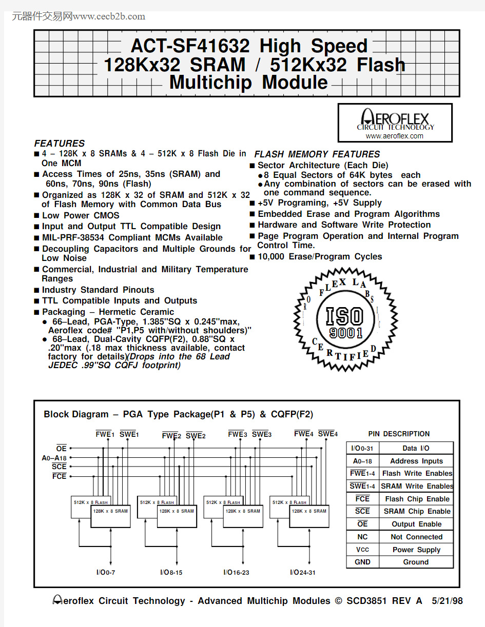
4 – 128K x 8 SRAMs & 4 – 512K x 8 Flash Die in One MCM
s Access Times of 25ns, 35ns (SRAM) and 60ns, 70ns, 90ns (Flash)
s Organized as 128K x 32 of SRAM and 512K x 32 of Flash Memory with Common Data Bus s Low Power CMOS
s Input and Output TTL Compatible Design s MIL-PRF-38534 Compliant MCMs Available
s Decoupling Capacitors and Multiple Grounds for Low Noise
s Commercial, Industrial and Military Temperature Ranges
s Industry Standard Pinouts
s TTL Compatible Inputs and Outputs s Packaging – Hermetic Ceramic
q 66–Lead, PGA-Type, 1.385"SQ x 0.245"max, Aeroflex code# "P1,P5 with/without shoulders)"q 68–Lead, Dual-Cavity CQFP(F2), 0.88"SQ x .20"max (.18 max thickness available, contact factory for details) (Drops into the 68 Lead JEDEC .99"SQ CQFJ footprint)
FLASH MEMORY FEATURES
s
Sector Architecture (Each Die)
q 8 Equal Sectors of 64K bytes each
q Any combination of sectors can be erased with one command sequence. s +5V Programing, +5V Supply
s Embedded Erase and Program Algorithms s Hardware and Software Write Protection
s Page Program Operation and Internal Program Control Time.
s 10,000 Erase/Program Cycles
ACT -SF41632 High Speed Multichip Module
128Kx32 SRAM / 512Kx32 Flash
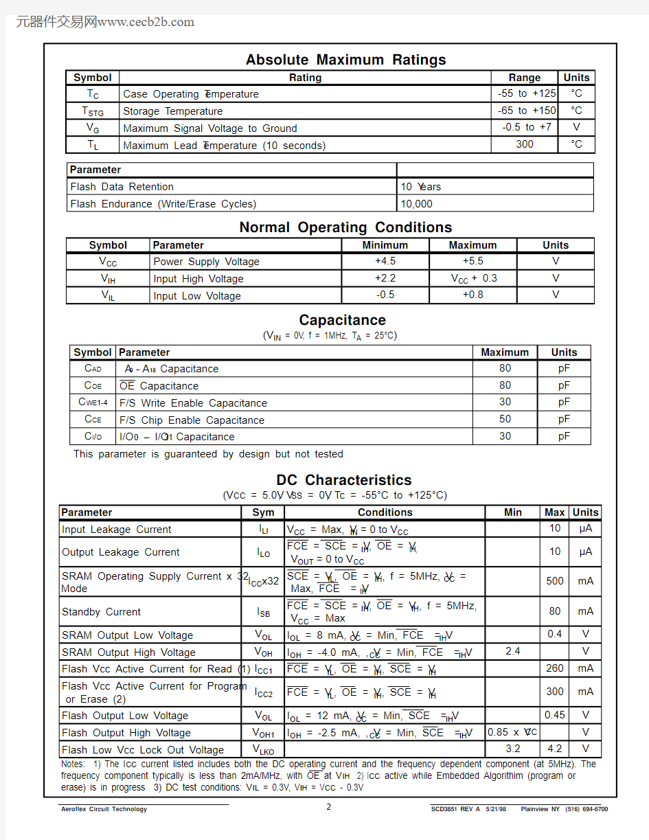
Absolute Maximum Ratings
Symbol Rating Range Units T C Case Operating T emperature-55 to +125°C T STG Storage Temperature-65 to +150°C V G Maximum Signal Voltage to Ground-0.5 to +7V T L Maximum Lead T emperature (10 seconds)300°C
Parameter
Flash Data Retention10 Y ears
Flash Endurance (Write/Erase Cycles)10,000
Normal Operating Conditions
Symbol Parameter Minimum Maximum Units
V CC Power Supply Voltage+4.5+5.5V
V IH Input High Voltage+2.2V CC + 0.3V
V IL Input Low Voltage-0.5+0.8V
Capacitance
(V IN = 0V, f = 1MHz, T A = 25°C)
Symbol Parameter Maximum Units
C A
D A0 – A18 Capacitance 80pF
C OE OE Capacitance80pF
C WE1-4F/S Write Enable Capacitance30pF
C CE F/S Chip Enable Capacitance50pF
C I/O I/O0 – I/O31 Capacitance30pF
This parameter is guaranteed by design but not tested
DC Characteristics
(V CC = 5.0V, V SS = 0V, Tc = -55°C to +125°C)
Parameter Sym Conditions Min Max Units Input Leakage Current I LI V CC = Max, V IN=0to V CC10μA
Output Leakage Current I LO FCE = SCE = V IH, OE = V IH,
V OUT=0to V CC
10μA
SRAM Operating Supply Current x 32 Mode I CC x32SCE = V IL, OE = V IH, f = 5MHz, V CC =
Max, FCE = V IH
500mA
Standby Current I SB FCE = SCE = V IH, OE = V IH, f = 5MHz,
V CC = Max
80mA
SRAM Output Low Voltage V OL I OL = 8 mA, V CC = Min, FCE = V IH0.4V SRAM Output High Voltage V OH I OH = -4.0 mA, , V CC = Min, FCE = V IH 2.4V Flash Vcc Active Current for Read (1)I CC1FCE = V IL, OE = V IH, SCE = V IH260mA
Flash Vcc Active Current for Program or Erase (2)I CC2FCE = V
IL
, OE = V IH, SCE = V IH300mA
Flash Output Low Voltage V OL I OL = 12 mA, V CC = Min, SCE = V IH0.45V Flash Output High Voltage V OH1I OH = -2.5 mA, , V CC = Min, SCE = V IH0.85 x V CC V Flash Low Vcc Lock Out Voltage V LKO 3.2 4.2V Notes: 1) The I CC current listed includes both the DC operating current and the frequency dependent component (at 5MHz). The frequency component typically is less than 2mA/MHz, with OE at V IH 2) I CC active while Embedded Algorithim (program or erase) is in progress 3) DC test conditions: V IL = 0.3V, V IH = V CC - 0.3V
SRAM AC Characteristics
(V CC = 5.0V, V SS= 0V, T C = -55°C to +125°C) Read Cycle
Parameter Symbol
–025
Min Max
–035
Min Max
Units
Read Cycle Time t RC2535ns Address Access Time t AA2535ns Chip Select Access Time t ACE2535ns Output Hold from Address Change t OH00ns Output Enable to Output Valid t OE1520ns Chip Select to Output in Low Z * t CLZ33ns Output Enable to Output in Low Z * t OLZ00ns Chip Deselect to Output in High Z * t CHZ1220ns Output Disable to Output in High Z * t OHZ1220ns * Parameters guaranteed by design but not tested
Write Cycle
Parameter Symbol
–025
Min Max
–035
Min Max
Units
Write Cycle Time t WC2535ns Chip Select to End of Write t CW2025ns Address Valid to End of Write t AW2025ns Data Valid to End of Write t DW1520ns Write Pulse Width t WP2025ns Address Setup Time t AS00ns Output Active from End of Write * t OW00ns Write to Output in High Z * t WHZ1020ns Data Hold from Write Time t DH00ns Address Hold Time t AH00ns * Parameters guaranteed by design but not tested
SRAM Truth Table
Mode SCE OE SWE Data I/O Power Standby H X X High Z Standby Read L L H Data Out Active Output Disable L H H High Z Active Write L X L Data In Active
Flash AC Characteristics – Read Only Operations (Vcc = 5.0V, Vss = 0V, Tc = -55°C to +125°C)
Parameter
Symbol
JEDEC Stand’d
–60
Min Max
–70
Min Max
–90
Min Max
Units
Read Cycle Time t AVAV t RC607090ns Address Access Time t AVQV t ACC607090ns Chip Enable Access Time t ELQV t CE607090ns Output Enable to Output Valid t GLQV t OE303535ns Chip Enable to Output High Z (1)t EHQZ t DF202020ns Output Enable High to Output High Z(1)t GHQZ t DF202020ns Output Hold from Address, CE or OE Change, Whichever is First t AXQX t OH000ns Note 1. Guaranteed by design, but not tested
Flash AC Characteristics – Write / Erase / Program Operations, FWE Controlled
(Vcc = 5.0V, Vss = 0V, Tc = -55°C to +125°C)
Parameter
Symbol
JEDEC Stand’d
–60
Min Max
–70
Min Max
–90
Min Max
Units
Write Cycle Time t AVAC t WC607090ns Chip Enable Setup Time t ELWL t CE000ns Write Enable Pulse Width t WLWH t WP404545ns Address Setup Time t AVWL t AS000ns Data Setup Time t DVWH t DS404545ns Data Hold Time t WHDX t DH000ns Address Hold Time t WLAX t AH454545ns Write Enable Pulse Width High t WHWL t WPH202020ns Duration of Byte Programming Operation t WHWH114TYP14TYP14TYPμs Sector Erase Time t WHWH2303030Sec Read Recovery Time before Write t GHWL000μs Vcc Setup Time t VCE505050μs Chip Programming Time505050Sec Chip Enable Hold Time t OEH1101010ns Chip Erase Time t WHWH3120120120Sec 1. Toggle and Data Polling only.
Flash AC Characteristics – Write / Erase / Program Operations, FCE Controlled
(Vcc = 5.0V, Vss = 0V, Tc = -55°C to +125°C)
Parameter
Symbol
JEDEC Stand’d
–60
Min Max
–70
Min Max
–90
Min Max
Units
Write Cycle Time t AVAC t WC607090ns Write Enable Setup Time t WLE L t WS000ns Chip Enable Pulse Width t ELEH t CP404545ns Address Setup Time t AVEL t AS000ns Data Setup Time t DVEH t DS404545ns Data Hold Time t EHDX t DH000ns Address Hold Time t ELAX t AH454545ns Chip Enable Pulse Width High t EHEL t CPH202020ns Duration of Byte Programming t WHWH114TYP14TYP14TYPμs Sector Erase Time t WHWH2303030Sec Read Recovery Time t GHEL000ns Chip Programming Time505050Sec Chip Erase Time t WHWH3120120120Sec
FWE
OE
FCE
Data
Addresses
5.0V
5555H PA
Data Polling
PA
D7
D OUT
PD
AOH
t WHWH 1
t AH
t AS
t DH
t CPH
t CP
t DS
t WS
t WC
t GHWL
Notes:
1. PA is the address of the memory location to be programmed.
2. PD is the data to be programmed at byte address.
3. D7 is the 0utput of the complement of the data written to the device.
4. D OUT is the output of the data written to the device.
5. Figure indicates last two bus cycles of four bus cycle sequence.
Write/Erase/Program Operation for Flash Memory, FCE Controlled
66 Pins — PGA-Type
Pin #Function Pin #Function Pin #Function Pin #Function 1I/O 818A 1535I/O 2552FWE 32I/O 919Vcc 36I/O 2653SWE 33I/O 1020FCE 37A 754GND 4A 1421SCE 38A 1255I/O 195A 1622I/O 339SWE 156I/O 316A 1123I/O 1540A 1357I/O 307A 024I/O 1441A 858I/O 298A 1825I/O 1342I/O 1659I/O 289I/O 026I/O 1243I/O 1760A 110I/O 127OE 44I/O 1861A 211I/O 228A 1745V CC 62A 312FWE 229FWE 146SWE 463I/O 2313SWE 230I/O 747FWE 464I/O 2214GND 31I/O 648I/O 2765I/O 2115I/O 1132I/O 549A 466
I/O 20
16A 1033I/O 450A 517
A 9
34
I/O 24
51
A 6
"P5" — 1.385" SQ PGA Type Special Order Package (without shoulders )
"P1" — 1.385" SQ PGA Type Package Standard (with shoulders on Pins 1, 11, 56 & 66) .220MAX
Bottom View (P1 & P5)
Side View (P1)
Side View (P5)
1.400 SQ 1.000.600 1.000.100 TYP
.020.016.100 TYP
Pin 56
Pin 66
Pin 11
Pin 1
MAX .020.016.100.025.035
.245MAX .165MIN
.145MIN
All dimensions in inches
TYP TYP
TYP
TYP
Ordering Information
Model Number DESC Part Number Speed Package ACT-SF41632N–26P1X TBD25(S) / 60(F) ns 1.385"sq PGA-Type ACT-SF41632N–37P1X TBD35(S) / 70(F) ns 1.385"sq PGA-Type ACT-SF41632N–39P1X TBD35(S) / 90(F) ns 1.385"sq PGA-Type ACT-SF41632N–26F2X TBD25(S) / 60(F) ns.88"sq CQFP ACT-SF41632N–37F2X TBD35(S) / 70(F) ns.88"sq CQFP ACT-SF41632N–39F2X TBD35(S) / 90(F) ns.88"sq CQFP Note: (S) = Speed for SRAM, (F) = Speed for FLASH
Aeroflex Circuit
Part Number Breakdown
Technology
Memory Type
SF = SRAM Flash Combo Module
Memory Depth, Locations
Pinout Options Memory Width, Bits
N = None
Memory Speed (Code)
Package Types & Sizes
Surface Mount Packages
F2 = 0.88"SQ 68 Leads Dual-Cavity CQFP
Thru-Hole Packages
P1 = 1.385"SQ PGA 66 Pins W/Shoulder
P5 = 1.385"SQ PGA 66 Pins WO/Shoulder
Screening
C = Commercial Temp, 0°C to +70°C
I = Industrial Temp, -40°C to +85°C
T = Military Temp, -55°C to +125°C
M = Military Temp, -55°C to +125°C Screened *
Q = MIL-PRF-38534 Compliant/SMD
*Screened to the individual test methods of MIL-STD-883
4 = 4M SRAM, 16 = 16M Flash
26 = 25ns SRAM & 60ns FLASH
37 = 35ns SRAM & 70ns FLASH
39 = 35ns SRAM & 90ns FLASH
ACT–SF41632N–26P1M
Aeroflex Circuit Technology
35 South Service Road
Plainview New York 11830
Telephone: (516) 694-6700
FAX: (516) 694-6715 Toll Free Inquiries: 1-(800) 843-1553
C I R C U I T T E C H N O L O G Y
Specifications subject to change without notice.