8002A音频IC 产品资料_矽源特科技
8002各脚电压

8002各脚电压在电子设备中,电压是一个非常重要的参数。
不同的电子元器件和电路板需要不同的电压来正常工作。
在数字电路中,最常用的电压是5V和3.3V,这两个电压可以满足大部分数字电路的需求。
然而,对于一些特殊的应用,可能需要其他的电压值。
在本文中,我们将讨论关于8002芯片的各脚电压。
8002是一款低压差线性稳压器芯片,主要用于电源管理和稳压控制。
它具有高效率、低功耗和低噪声等特点,广泛应用于手机、平板电脑、数码相机和其他便携式电子设备中。
我们来看看8002芯片的输入电压。
根据芯片规格书的说明,8002芯片的输入电压范围为2.7V至5.5V。
这意味着,我们可以将2.7V 至5.5V之间的任何电压作为8002芯片的输入电压。
当然,在实际应用中,我们应该选择适合具体应用场景的输入电压。
接下来,我们来看看8002芯片的输出电压。
8002芯片具有可调节的输出电压,可以满足不同的应用需求。
根据芯片规格书的说明,8002芯片的输出电压范围为0.8V至5.2V。
这意味着,我们可以将0.8V至5.2V之间的任何电压作为8002芯片的输出电压。
当然,在实际应用中,我们应该选择适合具体应用场景的输出电压。
除了输入电压和输出电压,8002芯片还有一些其他的电压参数需要注意。
例如,芯片的工作电流和待机电流。
根据芯片规格书的说明,8002芯片的工作电流一般在20mA至50mA之间,待机电流一般在1μA至10μA之间。
这些参数可以帮助我们评估芯片的功耗和使用寿命。
在使用8002芯片时,还需要注意一些电压的稳定性和精度问题。
根据芯片规格书的说明,8002芯片的输出电压稳定性一般在2%至5%之间,输出电压精度一般在1%至3%之间。
这些参数可以帮助我们评估芯片的性能和适用范围。
8002芯片的各脚电压参数非常重要。
在选择芯片和设计电路时,我们需要根据具体的应用需求来确定输入电压和输出电压。
同时,我们还需要考虑芯片的工作电流、待机电流、输出电压稳定性和精度等参数。
功放IC 8002

8002 DataSheet V1.0CONTENTSGeneral Description (4)Features (4)Applications (4)Typical Application Circuit (4)Absolute Maximum Ratings (5)Electrical Characteristics (5)Pin Configuration (6)Pin Layout (6)Pin Discription (6)Typical Characteristics (7)THD, THD+N,S/N (7)Power Supply Rejection Ratio (PSRR) (9)Power Dissipation (10)Output Power (11)Application Information (12)BLOCK DIAGRAM (12)BRIDGE CONFIGURATION EXPLANATION (13)POWER DISSIPATION (13)POWER SUPPLY BYPASSING (14)SHUTDOWN FUNCTION (14)PROPER SELECTION OF EXTERNAL COMPONENTS (14)Selection of Input Capacitor Size (15)AUDIO POWER AMPLIFIER DESIGN (15)A 1W/8Ω Audio Amplifier (15)Physical Size of Chip Package (17)FIGURE LISTFigure1. typical Audio Amplifier Application Circuit (4)Figure2. SOP Package Pin Distribution (6)Figure3. The block diagram of 8002 (12)Figure4. The Package of SOP-8 (17)TABLE LISTSTable1. Chip Limit Parameter Table (5)Table2. Electrical Characteristics (5)Table3. Pin Discription (6)General DescriptionThe 8002 is an audio power amplifier primarily designed for demanding applications in low-power portable systems. It is capable of delivering 3 watts of continuous average power to an 3ΩBTL load with less than 10% distortion (THD) from a 5VDC power supply. the 8002 does not require output coupling capacitors or bootstrap capacitors, and therefore is ideally suited for mobile phone and other low voltage applications where minimal power consumption is a primary requirement.the 8002 features a low-power consumption shutdown mode.the 8002 contains advanced pop & click circuitry which eliminates noise which would otherwise occur during turn-on and turn-off transitions. The 8002 is unity-gain stable and can be configured by external gain-setting resistorsFeaturesPower Output at 5.0V, 10% THD+N, 3Ω 3W (typ)Power Output at 5.0V,10% THD+N,4Ω 2.65W (typ)Power Output at 5.0V,10% THD+N,8Ω 1.8W (typ)Shutdown Current 0.6µA (typ)Available in space-saving packages: SOPImproved pop & click circuitry eliminates noise during turn-on and turn-off transitions2.20- 5.5V operationNo output coupling capacitors, snubber networks or bootstrap capacitors requiredUnity-gain stableExternal gain configuration capabilityApplicationsPortable computersDesktop computersLow voltage audio systemsTypical Application Circuitypical Audio Amplifier Application CircuitAbsolute Maximum RatingsChip Limit Parameter TableNameParameterSupply Voltage 6.0V Storage Temperature −65°C to +150°C Input Voltage −0.3V to VDD +0.3VESD Susceptibility 2000VJunction Temperature 150°CThermal ResistanceθJA 210°C/W θJC56°C/WWARNING: In addition to limits or any other conditions, the chip may be damaged.Electrical CharacteristicsThe following specifications apply for V DD =5V and R L =8Ω, unless otherwise specified. Limits apply for TA = 25°C.Electrical Characteristics8002SymbolParameter ConditionsTypical MaxUnits (Limits)V IN =0V,I O =0A, No load 6.510 mA I DD Quiescent Power Supply CurrentV IN =0V,I O =0A, 8load7.0 10 mA I OFF Shutdown Current0.8 2 uA V OS Outpt Offset Voltage5.7 30 mV R O Resistor Output8.5 10 K ΩOutput Power,3ΩLoad THD ≤1%,f=1KHz 2.3 Output Power,4ΩLoad THD ≤1%,f=1KHz 2 Output Power,8ΩLoad THD ≤1%,f=1KHz1.3 WOutput Power,3ΩLoadTHD+N ≤10%,f=1KHz 3 Output Power,4ΩLoad THD+N ≤10%,f=1KHz 2.56 P OOutput Power,8ΩLoadTHD+N ≤10%,f=1KHz 1.8 WT D Wake-up time100 mSTHD+N TotalHarmonicDistortion+Noise20Hz ≤ f ≤ 20kHz, A VD = 2R L = 8Ω, P O = 1W0.2 %PSRR Power Supply Rejection RatioV ripple =200mV sine P-P Input terminated With 10Ω 63(f=217Hz)67(f=1KHz)60 (min)dBPin ConfigurationPin LayoutSOP Package Pin DistributionPin DiscriptionTabl3. Pin DisnriptionPin NO.Pin Name Description1 SD The device enters in shutdown mode when a high level isapplied on this pin2 BYP Bypass capacitor pin which provides the common mode voltage3 +IN Positive input of the first amplifier, receives the common mode voltage4 -IN Negative input of the first amplifier, receives the audio inputsignal5 Vo1 Negative output6 VDD Analog VDD input supply.7 GND Ground connection for circuitry.8 Vo2 Positive outputTypical Characteristics THD, THD+N,S/NPower Supply Rejection Ratio (PSRR)Power DissipationPower Dissipaton vs Output Power,VDD=2.5VOutput PowerApplication InformationBLOCK DIAGRAMThe block diagram of 8002BRIDGE CONFIGURATION EXPLANATIONAs shown in Figure 1, the 8002 has two internal operational amplifiers. The first amplifier’s gain is externally configurable, while the second amplifier is internally fixed in a unity-gain, inverting configuration. The closed-loop gain of the first amplifier is set by selecting the ratio of Rf to Ri whilethe second amplifier’s gain is fixed by the two internal 20kΩ resistors. Figure 1 shows that the output of amplifier one serves as the input to amplifier two which results in both amplifiers producing signals identical in magnitude, but out of phase by 180°. Consequently, the differential gain for the IC isBy driving the load differentially through outputs Vo1 and Vo2, an amplifier configuration commonly referred to as “bridged mode” is established. Bridged mode operation is different from the classical single-ended amplifier configuration where one side of the load is connected to ground.A bridge amplifier design has a few distinct advantages over the single-ended configuration, as it provides differential drive to the load, thus doubling output swing for a specified supply voltage. Four times the output power is possible as compared to a single-ended amplifier under the same conditions. This increase in attainable output power assumes that the amplifier is not current limited or clipped. In order to choose an amplifier’s closed-loop gain without causing excessive clipping, please refer to the Audio Power Amplifier Design section.A bridge configuration, such as the one used in 8002,also creates a second advantage over single-ended amplifiers. Since the differential outputs, Vo1 and Vo2, are biased at half-supply, no net DC voltage exists across the load. This eliminates the need for an output coupling capacitor which is required in a single supply, single-ended amplifier configuration. Without an output coupling capacitor, the half-supply bias across the load would result in both increased internal IC power dissipation and also possible loudspeaker damage.POWER DISSIPATIONPower dissipation is a major concern when designing a successful amplifier, whether the amplifier is bridged or single-ended. A direct consequence of the increased power delivered to the load by a bridge amplifier is an increase in internal power dissipation. Since the 8002 has two operational amplifiers in one package, the maximum internal power dissipation is 4 times that of a single-ended amplifier.The maximum power dissipation for a given application can be derived from the power dissipation graphs or from Equation 1.It is critical that the maximum junction temperature TJMAX of 150°C is not exceeded. TJMAX can be determined from the power derating curves by using PDMAX and the PC board foil area. By adding copper foil, the thermal resistance of the application can be reduced from the free air value of θJA, resulting in higher PDMAX values without thermal shutdown protection circuitry being activated. Additional copper foil can be added to any of the leads connected to the 8002. It is especially effective when connected to VDD, GND, and the output pins. Refer to the application information on the 8002 reference design board for an example of good heat sinking. If TJMAX still exceeds 150°C, thenadditional changes must be made. These changes can include reduced supply voltage, higher load impedance, or reduced ambient temperature. Internal power dissipation is a function of output power. Refer to the Typical Performance Characteristics curves for power dissipation information for different output powers and output loading. POWER SUPPLY BYPASSINGAs with any amplifier, proper supply bypassing is critical for low noise performance and high power supply rejection. The capacitor location on both the bypass and power supply pins should be as close to the device as possible. Typical applications employ a 5V regulator with 10µF tantalum or electrolytic capacitor and a ceramic bypass capacitor which aid in supply stability. This does not eliminate the need for bypassing the supply nodes of the 8002. The selection of a bypass capacitor, especially CB, is dependent upon PSRR requirements, click and pop performance (as explained in the section, Proper Selection of External Components), system cost, and size constraints.SHUTDOWN FUNCTIONIn order to reduce power consumption while not in use, the 8002 contains shutdown circuitry that is used to turn off the amplifier’s bias circuitry. In addition, the 8002 contains a Shutdown Mode pin (LD and MH packages only), allowing the designer to designate whether the part will be driven into shutdown with a high level logic signal or a low level logic signal. This allows the designer maximum flexibility in device use, as the Shutdown Mode pin may simply be tied permanently to either VDD or GND to set the 8002 as either a "shutdown-high" device or a "shutdown-low" device, respectively. The device may then be placed into shutdown mode by toggling the Shutdown pin to the same state as the Shutdown Mode pin. For simplicity’s sake, this is called "shutdown same", as the 8002 enters shutdown mode whenever the two pins are in the same logic state. The MM package lacks this Shutdown Mode feature, and is permanently fixed as a ‘shutdown-low’ device. The trigger point for either shutdown high or shutdown low is shown as a typical value in the Supply Current vs Shutdown Voltage graphs in the Typical Performance Characteristics section. It is best to switch between ground and supply for maximum performance. While the device may be disabled with shutdown voltages in between ground and supply, the idle current may be greater than the typical value of 0.1µA. In either case, the shutdown pin should be tied to a definite voltage to avoid unwanted state changes.In many applications, a microcontroller or microprocessor output is used to control the shutdown circuitry, which provides a quick, smooth transition to shutdown. Another solution is to use a single-throw switch in conjunction with an external pull-up resistor (or pull-down, depending on shutdown high or low application). This scheme guarantees that the shutdown pin will not float, thus preventing unwanted state changes.PROPER SELECTION OF EXTERNAL COMPONENTSProper selection of external components in applications using integrated power amplifiers is critical to optimize device and system performance. While the 8002 is tolerant of external component combinations, consideration to component values must be used to maximize overall system quality. The 8002 is unity-gain stable which gives the designer maximum system flexibility. The 8002 should be used in low gain configurations to minimize THD+N+N values, and maximize the signal to noise ratio. Low gain configurations require large input signals to obtain a given output power. Input signals equal to or greater than 1Vrms are available from sources such as audio codecs. Please refer to the section, AudioPower Amplifier Design, for a more complete explanation of proper gain selection. Besides gain, one of the major considerations is the closedloop bandwidth of the amplifier. To a large extent, the bandwidth is dictated by the choice of external components shown in Figure 1. The input coupling capacitor, Ci, forms a first order high pass filter which limits low frequency response. This value should be chosen based on needed frequency response for a few distinct reasons.Selection of Input Capacitor SizeLarge input capacitors are both expensive and space hungry for portable designs. Clearly, a certain sized capacitor is needed to couple in low frequencies without severe attenuation. But in many cases the speakers used in portable systems, whether internal or external, have little ability to reproduce signals below 100Hz to 150Hz. Thus, using a large input capacitor may not increase actual system performance .In addition to system cost and size, click and pop performance is effected by the size of the input coupling capacitor, Ci. A larger input coupling capacitor requires more charge to reach its quiescent DC voltage (nominally 1/2 VDD). This charge comes from the output via the feedback and is apt to create pops upon device enable. Thus, by minimizing the capacitor size based on necessary low frequency response, turn-on pops can be minimized.Besides minimizing the input capacitor size, careful consideration should be paid to the bypass capacitor value. Bypass capacitor, CB, is the most critical component to minimize turn-on pops since it determines how fast the 8002 turns on. The slower the 8002’s outputs ramp to their quiescent DC voltage (nominally 1/2 VDD), the smaller the turn-on pop. Choosing CB equal to 1.0µF along with a small value of Ci (in the range of 0.1µF to 0.39µF), should produce a virtually clickless and popless shutdown function. While the device will function properly, (no oscillations or motorboating), with CB equal to 0.1µF, the device will be much more susceptible to turn-on clicks and pops. Thus, a value of CB equal to 1.0µF is recommended in all but the most cost sensitive designs.AUDIO POWER AMPLIFIER DESIGNA 1W/8Ω Audio Amplifier Given:Power OutputLoad ImpedanceInput LevelInput ImpedanceBandwidthA designer must first determine the minimum supply rail to obtain the specified output power. By extrapolating from the Output Power vs Supply Voltage graphs in the Typical Performance Characteristics section, the supply rail can be easily found.5V is a standard voltage in most applications, it is chosen for the supply rail. Extra supply voltage creates headroom that allows the 8002 to reproduce peaks in excess of 1W without producing audible distortion. At this time, the designer must make sure that the power supply choice along with the output impedance does not violate the conditions explained in the Power Dissipation section.1Wrms8Ω1Vrms20k Ω100Hz–20kHz ± 0.25dBOnce the power dissipation equations have been addressed, the required differential gain can be determined from Equation 2.From Equation 2, the minimum AVD is 2.83; use A VD = 3.Since the desired input impedance was 20kΩ, and with a A VD impedance of 2, a ratio of 1.5:1 of Rf to Ri results in an allocation of Ri = 20kΩ and Rf = 30kΩ. The final design step is to address the bandwidth requirements which must be stated as a pair of −3dB frequency points. Five times away from a −3dB point is 0.17dB down from passband response which is better than the required ±0.25dB specified.As stated in the External Components section, Ri in conjunction with Ci create a highpass filter.Use 0.39uf.The high frequency pole is determined by the product of the desired frequency pole, fH, and the differential gain, A VD. With a A VD = 3 and fH = 100kHz, the resulting GBWP = 300kHz which is much smaller than the 8002 GBWP of 2.5MHz. This figure displays that if a designer has a need to design an amplifier with a higher differential gain, the 8002 can still be used without running into bandwidth limitations.Physical Size of Chip PackageThe Package of SOP-8Dimensions In Millimeters Dimensions In Inches Symbol Min Max MinMax A 1.350 1.750 0.053 0.069 A 1 0.100 0.250 0.004 0.010 A 2 1.350 1.55 0.053 0.061 b 0.330 0.510 0.013 0.020 c 0.170 0.250 0.006 0.010 D 4.700 5.100 0.185 0.200 E 3.800 4.000 0.150 0.157 E1 5.800 6.2000.2280.244e 1.270(BSC) 0.050(BSC)L 0.400 1.270 0.016 0.050 θ0° 8°0° 8°。
矽普特产品简介
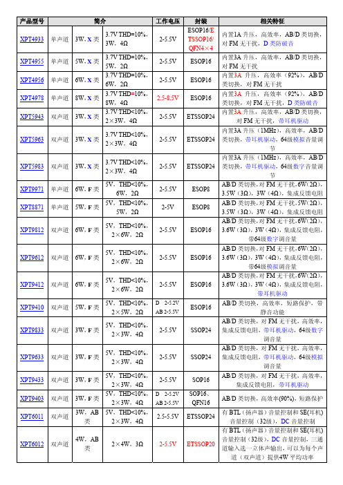
XPT5983 XPT9971 XPT8871 XPT9812
XPT9612
XPT9412 XPT9410 XPT9833
XPT9633 XPT9433 XPT9403 XPT6011
XPT6012
道(双声道)提供4W 平均功率
产品型号 XPT6013 XPT6871 XPT6875 XPT4809
XPT9863
XPT8863
XPT2008
XPT2069
XPT2068 C
XPT4098 XPT4871
F XPT4890 XPT4990 XPT0030 XPT4066 XPT4088 XPT4068 XPT6872
4 SOP18/SS OP24/SOP
16
SOP16/QF N16/DIP16 MSOP8/SO P8/ESOP8/
DFN8 MSOP8/SO
P8/DFN
WCSP9
MSOP8/ES OP8/SOP8/
DFN
WCSP
备注 单端模式,5V,THD+N≤0.5%,75mW (32Ω)。XPT4963的 SD 是高电平工作,
封装
ETSSOP20
SOP8
ESOP8
MSOP8/SO P8
SOP16/DIP 16/ETSSO P16/ETSS OP20 SOP16/ET SSOP20/DI P16
SOP8/ ESOP8
SOP16/DIP 16/ESOP16
SOP16/ES OP16/DIP1
6
QFN16/SO P16/DIP16
完全兼容 LM4861/8002 ,XPT4871H
WT8002功放芯片说明书.pdf
WT8002V1.00WT8002功放芯片说明书Note:WAYTRONIC ELECTRONIC CO.,LTD.reserves the right to change this document without prior rmation provided by WAYTRONIC is believed to be accurate and reliable.However,WAYTRONIC makes no warranty for any errors which may appear in this document.Contact WAYTRONIC to obtain the latest version of device specifications before placing your orders.No responsibility is assumed by WAYTRONIC for any infringement of patent or other rights of thirdparties which may result from its use.In addition,WAYTRONIC products are not authorized for use as critical components in V1.02一.概述WT8002是一款音频功率放大芯片.工作电压2V~6V,以BTL的方式输出,它內含降低上电瞬间与启动/关闭产生pop声的电路与过温保护,低待机电流0.5uA二、特性内置降低上电瞬间与启动/关闭产生pop声的电路增益可由外挂电阻调节宽广的工作电流:1.6V-6V封装形式:SOP-8高輸出功率Pout= 1.2W(VDD=5V,THD+N=1%,8ohm)Pout=2W(VDD=5V,THD+N=1%,4ohm)三、应用可应用于手提设备,台式电脑及低电压工作的音频设备四、功能特性桥路设置WT8002内部共有2个运放工作,第一个运放增益可在外部用RF和RJ两个电阻进行设置(+IN 和-IN端口),第二个运放的增益由内部固定不变。
8002音频功放IC规格书 矽源特科技
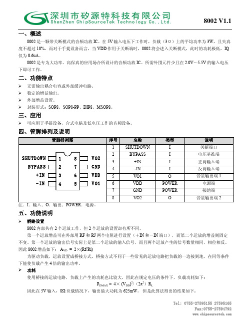
Tel: 0755-27595155 27595165 Fax:0755-27594792
DIP-8
1 .5 5 0 .1
3 .3 0 2
1 .2 7 4 .9 0 .4 2
2 .4 1 3
3 .9
6 .0
8002 V1.1
0 .2 1
Tel: 0755-27595155 27595165 Fax:0755-27594792
类型 I I I I O
POWER POWER
O
说明 关断端口 电压基准端 正向输入端 反向输入端 音量输出端 1 电源端 接地端 音量输出端 2
¾ 桥路设置 8002 内部共有 2 个运放工作,但 2 个运放的设置却有所不同。 第一个运放增益可在外部用 RF 和 RJ 两个电阻进行设置(+IN 和-IN 端口),而第二个运放的增益则固定
四、管脚排列及说明
管脚排列图
S HU TD OW N
1
8
V O2
B YP AS S
2
7
G ND
+ IN
3
6
V DD
- IN
4
5
V O1
注:I:输入;O:输出;POWER:电源。
五、功能说明
序号 1 2 3 4 5 6 7 8
名称 SHUTDOWN
BYPASS +IN -IN VO1 VDD GND VO2
在很多应用场合,关断端的电平转换都是由处理器来完成的。当使用单向闸刀开关实现电平转换时,可以在
关断端加上拉电阻,这样当开关关断时,因上拉电阻的作用,使得 8002 关断端的电平处于一个正确的状态,以保 证 8002 不会进入错误的工作状态。
SD8002A 3W 单声道带关断模式音频功率放大器

SD8002A3W 单声道带关断模式音频功率放大器DatasheetVersion 1.0Shouding3W 单声道带关断模式音频功率放大器SD8002A SD8002A SD8002A SD8002A SD8002A3W 单声道带关断模式音频功率放大器一.概述是一种桥工音频功率放大器,使用5V 电源,且THD+N≤1.0%时,能给一个4Ω的负载提供2W 的平均功率。
音频功率放大器是为提供高质量的输出功率而设计的,需要很少的外围设备,便可以提供高品质的输出功率。
不需要输出耦合电容,具有高电平关断模式,非常适合低功耗的便携式系统。
可以通过外部电阻控制增益,并有补偿器件保证芯片的正常工作。
二. 重要规格1.1KHz ,接4Ω负载(),平均输出功率为2W ,THD+N 1%(典型) 2.1kHz ,接4Ω负载,平均输出功率为3W ,THD +N 10%(典型) 3.关断电流 0.6 μA (典型) 4.输入电压范围 2.0~5.5V三.特征1. 无输出耦合电容2. 外部电阻可调增益3. 整体增益稳定4. 热敏关断保护电路5. 小尺寸 (SOP-8)封装形式四.应用1. 个人电脑2. 便携式消费类电子产品3. 无源扬声器4. 玩具及游戏机3W 单声道带关断模式音频功率放大器Shouding五.芯片封装引脚分布六.典型应用3W 单声道带关断模式音频功率放大器Shouding七.绝对最大额定值电源电压 6.0V 焊接信息存储温度 -65℃~+ 150℃ 气化态(60秒) 215 ℃输入电压 -0.3V ~V DD +0.3V 红外线(15秒) 220℃ 功耗 内部限制 热阻ESD 磁化系数(人体模型) 3000V θJC (典型) 35°C/W ESD 磁化系数(机器模型) 250V θJA (典型) 140°C/W 结温 150℃八.工作额定值温度范围:T MIN ≤T A ≤T MAX -40 ℃≤T A ≤+ 85℃ 电源电压 2.0V ≤V DD ≤5.5V3W 单声道带关断模式音频功率放大器Shouding九.电学特性1、除非另外指明,以下都是V DD =5V ,R L =8Ω, 限制应用在TA =25℃MD4871 符号 参数 条件 标准 限制单位 (限制)2.0 V (最小) V DD 电源电压2.5 V (最大)I DD 静态电流 V IN = 0V , I O =0A 3.5 8 mA (最大) I SD 关断电流 V SD =V DD , V IN =0V 0.6 2 μAV OS输出失调电压V IN = 0V5.0 50.0mV (最大)THD=1%(最大);f=1KHzR L =4Ω R L =8Ω 2 1.2 WP O输出功率THD=10%(最大);f=1KHzR L =4Ω R L =8Ω3 2WPSRR 电源抑制比 V DD =4.9V ~5.1V 65 dBTHD+N 总谐波失真 20Hz ≤f ≤20KHz R L =4Ω,P O =1.6W R L=8Ω, P O =1W0.10.1%十、外围元器件描述器件 功能描述1.R i 与R f 一起设置闭环增益的输入电阻,同时还与C I 形成了高通滤波器,且f C =1/(2πR I C I )。
功率放大器8002芯片基本结构描述

文章标题:探秘功率放大器8002芯片:基本结构揭秘一、引言功率放大器8002芯片,作为音频功率放大器领域的重要组成部分,其基本结构和工作原理一直备受关注。
本文将从8002芯片的基本结构出发,深入解析其组成和功能,帮助读者全面理解这一重要器件。
二、8002芯片的基本构造1. 芯片外部形状:8002芯片通常采用DIP-8封装,包括8个引脚,外形小巧玲珑却功能强大。
2. 内部器件构成:8002芯片内部包括了多个功能模块,包括输入级、驱动级和输出级等,每个部分都承担着不同的功能。
三、8002芯片的工作原理1. 输入级:8002芯片的输入级主要负责接收外部音频信号,并对其进行放大和处理,为后续级别提供合适的信号源。
2. 驱动级:驱动级是8002芯片的核心部分,它负责将输入的信号放大,并驱动功放芯片的输出级,保证输出级得到稳定的驱动信号。
3. 输出级:8002芯片的输出级将来自驱动级的信号经过二次放大和滤波,输出给扬声器,从而实现音频信号的放大和放大。
四、8002芯片的应用领域8002芯片由于其优秀的性能和稳定的工作特性,在音频功率放大器领域得到了广泛的应用。
无论是消费类电子产品中的音箱、手机等,还是工业控制系统中的音频放大器模块,都离不开8002芯片的支持。
五、结论与展望功率放大器8002芯片的基本结构和工作原理,本文进行了深入的剖析和阐释。
通过本文的阅读,相信读者已经对这一重要器件有了全面的了解和认识。
未来,随着技术的不断进步,8002芯片将会迎来更广阔的应用空间,也希望它能为音频领域的发展贡献更多的力量。
六、个人观点与理解在笔者看来,功率放大器8002芯片作为音频领域的重要器件,其基本结构紧凑、功能全面,能够满足不同场景的音频放大需求。
随着智能化、数字化的发展,8002芯片将会迎来更多的创新应用,为人们带来更加优质的音频体验。
以上内容为文章的主要结构和内容,希望对您有所帮助。
在8002芯片的基本结构和工作原理的基础上,我们可以进一步探讨其在音频功率放大器领域的具体应用和未来发展趋势。
8002a功放芯片参数
8002a功放芯片参数8002A功放芯片参数1. 引言功放芯片是一种用于放大电信号的集成电路。
8002A功放芯片是一种常见的功放芯片,广泛应用于电子产品中。
本文将详细介绍8002A功放芯片的参数及其作用。
2. 8002A功放芯片概述8002A功放芯片是一种双路单声道功放芯片,采用BTL(平衡型连接方式)设计,适用于3V至12V的供电电压。
它具有低功耗、低噪声、高音质等优点,广泛应用于MP3播放器、手机音频放大、电子琴等电子产品中。
3. 电源参数8002A功放芯片的工作电源电压范围为3V至12V。
在3V供电电压下,输出功率约为300mW。
当供电电压达到12V时,输出功率可达4W。
此外,8002A功放芯片的静态电流非常低,仅为6mA左右,因此它非常适合低功耗的电子设备。
4. 输出参数8002A功放芯片的输出功率范围为300mW至4W。
它能够提供稳定的音频输出信号,具有较低的失真和噪声。
该芯片的输出电阻为8Ω,适用于8Ω阻抗的扬声器。
5. 控制参数8002A功放芯片具有灵活的控制参数,可以通过外部电阻来调整放大倍数。
通常情况下,通过控制输入信号的幅度,可以控制功放芯片的放大倍数。
此外,该芯片还具有短路保护功能,能够保护耳机或扬声器免受电流过大的损害。
6. 输入参数8002A功放芯片的输入电阻为30kΩ。
它采用单端输入方式,对于输入信号具有良好的接收能力。
此外,该芯片还具有一定的输入电容,可以阻隔直流偏置,从而提高音频的输出质量。
7. 应用领域8002A功放芯片广泛应用于各种消费电子产品中。
它常见的应用领域包括但不限于以下几个方面:(1)MP3/MP4播放器: 8002A芯片提供了较好的音频放大效果,使得MP3/MP4播放器具备更好的音质输出。
(2) 手机音频放大:由于8002A芯片具有低功率消耗和低噪音等优点,适合用于手机音频放大,提高音质和音量输出。
(3) 电子琴: 8002A芯片能够提供稳定的音频放大效果,使得电子琴具备更好的音质和音量效果。
- 1、下载文档前请自行甄别文档内容的完整性,平台不提供额外的编辑、内容补充、找答案等附加服务。
- 2、"仅部分预览"的文档,不可在线预览部分如存在完整性等问题,可反馈申请退款(可完整预览的文档不适用该条件!)。
- 3、如文档侵犯您的权益,请联系客服反馈,我们会尽快为您处理(人工客服工作时间:9:00-18:30)。
7
G ND
+ IN
3
6
V DD
- IN
4
5
V O1
注:I:输入;O:输出;POWER:电源。
五、功能说明
序号 1 2 3 4 5 6 7 8
名称 SHUTDOWN
BYPASS +IN -IN VO1 VDD GND VO2
类型 I I I I O
POWER POWER
O
说明 关断端口 电压基准端 正向输入端 反向输入端 音量输出端 1 电源端 接地端 音量输出端 2
VDD=4.9V~5.1V
Tel: 0755-27595155 27595165 Fax:0755-27594792
八、特性参数
8002A V1.1
Tel: 0755-27595155 27595165 Fax:0755-27594792
¾ 桥路设置 8002A 内部共有 2 个运放工作,但 2 个运放的设置却有所不同。 第一个运放增益可在外部用 RF 和 RJ 两个电阻进行设置(+IN 和-IN 端口),而第二个运放的增益则固定
不变。第一个运放的输出信号实际上是第二个运放的输入信号,而且两个运放产生的信号数量相同,相位相反。 因此 8002A 增益如下: AVD = 2×(Rf/Ri)
为驱动负载,运放设置成桥接方式。桥接方式不同于一些常见的运放电路把负载的一边接到地,在同等条件 下能使负载产生 4 倍的输出功率。 ¾ 功耗
使用桥接的运放电路,负载上产生的功耗也比较大,因此在规定电压的条件下,负载功耗如下: PDMAX = 4× (VDD)2/(2π2)RL
因此在 5V 输入,8Ω 负载情况下,输出最大功耗为 625mW。 但是此算法得出的结果如下:
Tel: 0755-27595155 27595165 Fax:0755-27594792
8002A V1.1
PDMAX = (TJMAX-TA)/ θJA 注:SOP 封装θJA=140°C/W,DIP 封装θJA=107°C/W,MSOP 封装θJA=210°C/W ¾ 基准电压
在很多应用场合,关断端的电平转换都是由处理器来完成的。当使用单向闸刀开关实现电平转换时,可以在
关断端加上拉电阻,这样当开关关断时,因上拉电阻的作用,使得 8002A 关断端的电平处于一个正确的状态,以 保证 8002A 不会进入错误的工作状态。
六、极限参数(Ta=25℃)
特性
符号
范围
单位
工作电压 输入电压 工作温度 环境温度 节点温度
电压基准端的外接电容应尽可能的靠近 8002A,0.1μF 的电容提高了内部偏置电压的稳定性并且减少了 PSRR 的影响。可以通过加大 BYPASS 端的对地电容值来改善 PSRR。CB 值的大小取决于对 PSRR 的要求。 ¾ 关断功能
为了减少功耗,8002A 的关断端可以关闭外部的偏置电路。当关断端为高电平时,运放关闭,8002A 不工 作,这时 8002A 的工作电流降低到 0.6uA。当关断端电压略低于 VDD 时,8002A 工作状态不稳定。所以,关断端 应置于一个稳定的电压值,以免 IC 进入错误的工作状态。
二、功能特点
¾ 无需输出耦合电容或外部缓冲电路。 ¾ 稳定的增益输出。 ¾ 外部增益设置。 ¾ 封装形式:SOP8、SOP8-PP、DIP8、MSOP8。
三、应用
¾ 可应用于手提设备,台式电脑及低电压工作的音频设备。
四、管脚排列及说明
管脚排列图
S HU TD OW N
1
8
V O2
B YP AS S
2是一颗带关断模式的音频功放 IC。在 5V 输入电压下工作时,负载(3Ω)上的平均功率为 3W,且失 真度不超过 10%。而对于手提设备而言,当 VDD 作用于关断端时,8002A 将会进入关断模式,此时的功耗极 低,IQ 仅为 0.6uA。
8002A 是专为大功率、高保真的应用场合所设计的音频功放 IC。所需外围元件少且在 2.0V~5.5V 的输入电 压下即可工作。
Tel: 0755-27595155 27595165 Fax:0755-27594792
DIP-8
1 .5 5 0 .1
3 .3 0 2
1 .2 7 4 .9 0 .4 2
2 .4 1 3
3 .9
6 .0
8002A V1.1
0 .2 1
Tel: 0755-27595155 27595165 Fax:0755-27594792
VDD VIN TOPR TA TJ
6
V
-0.3~VDD+0.3
V
-65~+150
℃
-40~+85
℃
150
℃
七、电气参数(VDD=5V,RL=8Ω,Ta=25℃)
名称
符号 最小值 典型值
工作电压 静态电流 关断电流 输出偏压
VDD
2.0
--
IDD
--
6.5
ISD
--
0.6
VOS
--
5.0
输出功率
--
MSOP8
8002A V1.1
Tel: 0755-27595155 27595165 Fax:0755-27594792
1.2
PO
--
1.5
总谐波失真+噪音 THD+N
--
0.25
电源抑制比
--
60
最大值 5.5 10 2 50 -----
单位 V mA uA mV
W
% dB
测试条件
VIN=0V, IO=0mA VPIN1=VDD VIN=0V
THD=1%, f=1KHz, RL=8Ω THD=10%, f=1KHz, RL=8Ω 20Hz≤f≤20KHz, AVD=2, RL=8Ω, PO=1W
NC
Cs + 1 .0 uF T an t
4 -IN 3 +IN +
6
4 0K Ω 100KΩ 40KΩ
2 Bypass
V DD /2
A V= -1 +
1 Shutdown Bias
1 00 KΩ
G ND
7
VO1 5 VO2 8
十、封装尺寸图
SOP-8
8002A V1.1
RL 8Ω
SOP8-PP(带散热片)
8002A V1.1
Tel: 0755-27595155 27595165 Fax:0755-27594792
九、电路原理图
V DD
Rf 2 0K Ω
A ud io I np ut
Ci 0 .3 9u F
+
Ri 2 0K Ω
V DD
CB
RP U
1 .0 uF