红米Note3 全网通版原理框图
红米手机 原理图 红米 电路图原理图
GPIO_0
NC
GPIO_41
WCSS_WLAN_DATA_1
GPIO_1
NC
GPIO_42
WCSS_WLAN_DATA_0
GPIO_2
NC
D
GPIO_3
NC
GPIO_43 GPIO_44
WCSS_WLAN_SET WCSS_WLAN_CLK
GPIO_4
UART_MSM_TX
GPIO_45
WCSS_FM_SSBI
5
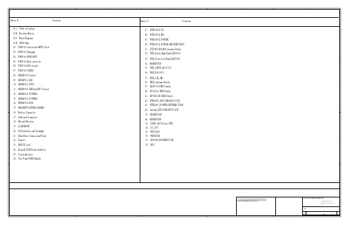
Sheet #
Content
01A. Table of Content 01B. Revision History
D
01C. Block Diagram 01D. GPIO Map 02. PM8916 Control and MPP/Clock 03. PM8916 Charging 04. PM8916 GPIO/MPP 05. PM8916 Buck converter 06. PM8916 LDO circuits 07. PM8916 CODEC 08. MSM8916 Control 09. MSM8916: EBI 10. MSM8916: GPIO
GPIO_79
WTR1_SWITCH_CTL1
GPIO_39
WCSS_BT_SSBI
GPIO_80
WTR0_RX_ON
GPIO_40
WCSS_WLAN_DATA_2
GPIO_81
WTR0_RF_ON
GPIO_82 GPIO_83 GPIO_84 GPIO_85 GPIO_86 GPIO_87 GPIO_88 GPIO_89 GPIO_90 GPIO_91 GPIO_92 GPIO_93 GPIO_94 GPIO_95 GPIO_96 GPIO_97 GPIO_98 GPIO_99 GPIO_100 GPIO_101 GPIO_102 GPIO_103 GPIO_104 GPIO_105 GPIO_106 GPIO_107 GPIO_108 GPIO_109 GPIO_110 GPIO_111 GPIO_112 GPIO_113 GPIO_114 GPIO_115 GPIO_116 GPIO_117 GPIO_118 GPIO_119 GPIO_120 GPIO_121
最强安卓手机小米3联通版拆机评测
最强安卓手机小米3联通版拆机评测发布时间:2014-01-10 18:39 作者:电脑百事网来源:图文iT168 526次阅读最近关于小米联通版更换处理器、更换摄像头的话题在网上热议,有人说更换了处理器的小米3将不能支持4G网络,还有人说,小米3联通版采用了上一代背照式摄像头,而不是宣传的堆栈式摄像头,到底谁对谁错呢,今天百事网小编为大家带来小米3联通版拆机图解,用实践来说话。
最强安卓手机小米3联通版拆机评测其实我们之前也拆解过首批小米3,不过首批小米3属于移动版,内部处理器与联通版不同。
不过不管是移动版还是联通版,其外观设计,内部结构都是一样的,因此拆解方法与步骤也基本相同。
首先是需要拆解下顶部的两颗螺丝,然后是打开通过卡扣和前部面板卡在一起的后盖。
值得一提的是,在小米3顶部SIM卡槽的螺丝上覆盖了易碎贴,也就是谁拆解第一步就会失去保修功能,因此大家千万不要随意尝试拆机喔。
小米3联通版拆机细节小米3联通版拆机入口拆开后盖后,我们就可以看到,小米3联通版和移动版内部布局大致相同,在外壳内部覆盖了石墨散热层,石墨拥有高比热容,能够起到为芯片散热的作用,这也是小米从小米1时代开始就使用的一个散热技术。
小米3联通版拆机背壳内部小米3并没有采用了超薄设计,外观上也谈不上造型新颖,其中有一个原因在于小米3内部的无线设计,小米3联通版这种天线设计,信号表现肯定会较为出色。
电池方面,小米3联通版搭载了3050mAh电池,这在5英寸屏幕中算的上中偏上水平,续航方面,小米3联通版会有比较不错的表现。
图为小米3联通版内部电池拆解小米3内部机身底部配备了信号天线、扬声器、通话麦克风和支持OTG功能的MicroUSB数据充电接口,值得一提的是,在小米2消失的虚拟按键背光终于回到了小米3身上。
图为小米3联通版拆机细节特写我们本次拆解的应该是小米3联通版的首批机器,可以看到,及时首批的小米3联通版,依旧是12面12月生产的,这样看来,小米3联通版并不是有货不发,确实是在等高通800AB处理器量产。
小米红米Note 3技术评测说明书

TECHNICAL REVIEW OF XIAOMI’S NEW REDMI NOTE 3 SMARTPHONE FOR INDIAEXECUTIVE SUMMARYThe midrange smartphone market is experiencing huge growth, especially in China and India. The midrange has become a focal point for many smartphone vendors and the chipmakers that supply them. Companies like Xiaomi are launching devices with help from chip vendors like Qualcomm and MediaTek. The Xiaomi Redmi Note 3, featuring the new Snapdragon 650 SoC, is optimized for performance and energy efficiency.The original Redmi Note 3, launched in China in November 2015, had similar specifications to the new Redmi Note 3 for India announced in March 2016, but looks can be deceiving. The new Redmi Note 3 is different than its seemingly identical “brother”. The Redmi Note 3 packs more features than one would expect at its price. The new model uses a Qualcomm Snapdragon 650 processor, rather than the MediaTek Helios X10 chips found in many phones in the sub Rs 15,000 price range. The new Redmi Note 3 falls in the midrange of the smartphone market. Given the changing market dynamics and phone capabilities, Moor Insights & Strategy (MI&S) tested the Redmi Note 3 with the Snapdragon 650 to provide a technical platform overview. This paper compares the new chip and phone against alternative platforms. The analysis focuses primarily on key silicon components and uses benchmarks to evaluate CPU, GPU, memory, and storage performance.PRODUCT OVERVIEWXiaomi is bringing this new version of the Redmi Note 3 to India to address the needs of the typical Indian phone enthusiast in the Rs 10,000 to 15,000 range. The Redmi Note 3 has a 6core processor, 5.5” 1080p screen, aluminum unibody, fingerprint sensor, 16MP camera, 802.11ac WiFi, 4G LTE, and a 4,000 mAh battery. These specs make the Xiaomi Redmi Note 3 competitive in the targeted price range, and they offer another choice to Indian consumers for longer battery life and more performance.Xiaomi’s switch from the MediaTek Helios X10 to a Qualcomm Snapdragon 650 is an upgrade to a 6core CPU configuration with two A72 cores and four A53 cores. It also comes with a significant upgrade to the GPU, DSP, and modem. The Snapdragon 650 comes with an Adreno 510 GPU, which is the same family of GPUs in the Snapdragon820 with an Adreno 530. The modem in the Redmi Note 3 is capable of 150 Mbps download and 50 Mbps upload speeds. Qualcomm’s embedded X8 LTE modem prepares the Redmi Note 3 for the growing LTE market within India, potentially futureproofing it for years to come.DESIGN & BUILD QUALITYAlthough this paper is a mostly technical review focused on performance and battery life, we noticed the Redmi Note 3 has a full aluminum body and smooth curved edges for a comfortable feel in the hand. This industrial design projects a more “premium” image. In addition, Xiaomi included a Fingerprints FPC1022 fingerprint sensor for easeofaccess and biometric security. We did not explore the design, security or responsiveness of the fingerprint sensor. Xiaomi opted for a microUSB 2.0 connector versus USB TypeC, which may draw ire from some enthusiasts. But a USB TypeC cable would add cost, and as a Google engineer has shown, several commercially available USB TypeC cables are not safe or do not support the claimed speeds. DISPLAY & CAMERASThe Xiaomi Redmi Note 3 features a 5.5” LCD display with 1080p resolution. This resolution and display size translate to about 403 ppi. Because the Redmi Note 3 is targeted at a more affordable segment, it does not feature a 1440p display or OLED display technology. Xiaomi reserves those features for highend phones, like the Mi Note Pro, which costs roughly twice as much as the Redmi Note 3. With a 1080p display, the Redmi Note 3 takes advantage of Qualcomm’s Adreno 510 GPU and allows for “bestinclass”, midrange GPU performance.The Redmi Note 3 has a decent camera, featuring a Samsung f/2.0 16MP primary camera and an f/2.0 5MP frontfacing camera. The camera itself is not unique compared to other cameras on phones at this price point, but it does launch fairly quickly and takes acceptable photos. It does not have the sophisticated manual camera capabilities more common on highend phones.PERFORMANCE & BENCHMARKSTo test the new Xiaomi Redmi Note 3’s performance, MI&S ran a series of technical benchmarks. Based on its specifications, the Redmi Note 3 should be one of the longest lasting phones on the market, if not in the world. Design, hardware integration, and software are important, but great specifications do not always equate to greatexperiences or performance. MI&S tested CPU, GPU, memory, and storage subsystem performance.Xiaomi supplied MI&S with an early sample of the new Redmi Note 3. Our testing looked at synthetic and real world applications, including some of the most popular apps in India on Google Play like Facebook, Facebook Messenger, Truecaller, MX Player, and WhatsApp. MI&S also ran some performance and efficiency benchmarks that an Indian enthusiast might expect to see. MI&S ran a combination of industry standard benchmarks like 3DMark (v1.5.3285), PCMark for Android (v1.3.3083), and Geekbench 3.0 (v3.4.1) as well as Basemark’s new Power Analysis Tool v1.0.Basemark’s Power Assessment Tool (PAT) measures how much power the entire device uses to the milliwatt and millisecond. It measures how long an application is running on the application processor and how much power it causes the phone to draw. PAT combines hardware and software and tests a device’s power consumption and time to process workloads. This review uses PAT to evaluate realworld applications in both how long processed takes (seconds) and how much power they drawn (watts), thus leading to total energy consumed by each application run and what affects battery life (mAh: milliwatt amp hours).We compared the Xiaomi Redmi Note 3 to the LeEco Le 1s, which also sells in India. The LeEco Le 1s phone features the familiar MediaTek Helios X10 SoC and is a good basis for devicetodevice and SoCtoSoC comparisons. Prior to testing, we ensured that both devices were running the latest versions of their operating systems and that their displays were set to auto brightness, since these are the conditions under which most users will operate their devices. The only time the devices were taken off auto brightness was to run PCMark for Android’s battery life test. The Redmi Note was uptodate with Android 5.1.1, and the LeEco was uptodate to 5.0.2, both the latest Android versions for each device.CPU & SYSTEM PERFORMANCEGeekbench is one of the most commonly used benchmarks for comparing CPU performance. There are large differences between the Redmi Note 3’s Snapdragon 650 and the LeEco Le 1s’s Helios X10. Most notably, the A72 core in the Redmi Note 3 allows for a much higher single core performance, while the 8 total cores in the LeEco Le 1s allow it to perform better in Geekbench’s multicore test. However, the multicore test is less relevant than the single core, because many Android apps and most apps in general are singlethreaded.FIGURE 1: CPU PERFORMANCE Single CoreMultiCore 0100020003000400050006000152536759635082Geekbench 3(higher is better)Xiaomi Redmi Note 3LeEco Le 1s Next, MI&S tested a holistic system benchmark with Basemark OSII system benchmark. FIGURE 2: HOLISTIC SYSTEM BENCHMARK System Memory Graphics WebOverall 05001000150020002500212216431623929151417901186467793942Basemark OSII(higher is better)Xiaomi Redmi Note 3LeEco Le 1s The Redmi Note 3 with the Snapdragon 650 beats the LeEco Le 1s with the MediaTek X10. In the graphics test, the differences are several hundred percent. After all subtests, the new Snapdragon 650 in the Redmi Note 3 is at least 50% faster than the MediaTek X10 in the LeEco Le 1s.Snapdragon 650 performance is reinforced by the PCMark for Android benchmark: 5257 for the Redmi Note 3 versus 4445 for the LeEco Le 1s.FIGURE 3: PCMARK FOR ANDROID Xiaomi Redmi Note 3LeEco Le 1s 010002000300040005000600052574445PC Mark Work(points higher is better)GRAPHICSIn 3D graphics benchmarks, the Xiaomi Redmi Note 3 outperformed the LeEco Le 1s. FIGURE 4: 3D GRAPHICS Manhattan 3.1TRexALU 2Driver Overhead 205101520253035409.73420124.51615 5.2GFX BenchXiaomi Redmi Note 3LeEco Le 1sIn GFX Bench, the Redmi Note 3 dominates the tests, winning some by triple digitpercentages. This can be directly attributable to the Snapdragon 650’s Adreno 510 GPU which is designed for high performance compared to the Helios X10 and PowerVR G6200 GPU.MI&S also ran the industry standard 3DMark and Basemark X benchmarks. InBasemark X the Snapdragon 650’s Adreno 510 scored 15,037 points while the X10’s PowerVR G6200 scored 7,987, just a little over half the performance. We saw a similarresult in 3DMark with the Snapdragon 650’s Adreno 510 GPU scoring 867 points and the MediaTek X10’s PowerVR G6200 scoring only 453. These scores reinforce the Redmi Note 3’s superior GPU performance at its price point.We also ran AnTuTu. While MI&S does not consider AnTuTu to be as well documented, tightly managed, or monitored for fraud like the benchmarks mentioned above, many Indian enthusiasts may still expect to see the results. AnTuTu has improved its benchmark’s tests and weighting over time, but it will need to continue to improve before we fully consider it on par with the others. Nonetheless, we are providing results to meet informational expectations. The Redmi Note 3 scored 76,140 points while the LeEco Le 1s scored 51,368 points, so according to AnTuTu, the Redmi Note 3 is 50% faster than the LeEco Le 1s.FIGURE 5: ANTUTUPOWERIn addition to the synthetic benchmarks above, MI&S also ran Basemark PAT to measure how long an application took to run, at what power level, and how much total energy it used. The Redmi Note 3 idled at 1.5 watts at the Android desktop, while the LeEco Le 1s idled at 1.7W. With the screen off, the Redmi Note 3 idled at 150 mW, while the LeEco Le 1s did the same at roughly 300 mW.The Redmi Note 3 took 6.0 seconds to load the Facebook application at an average power of 2.6W or 15.6 joules (J). The LeEco Le 1s accomplished the same task in 6.2 seconds at 2.9W or 17.98J—15% more energy and slightly slower.FIGURE 6: BASEMARK POWER ASSESSMENT TOOL PORTIONThe Redmi Note 3 loaded Facebook Messenger in 2 seconds with 3.1W average power (6.2J), while the LeEco Le 1s took 4 seconds at 2.6W (10.4J)—twice as long with 68% more energy. WhatsApp loaded on the Redmi Note 3 in 2 seconds at 2.4W average power (4.8J); the LeEco Le 1s also took 2 seconds but at 3.3W (6.6J)—a difference of 37%. The Redmi Note 3 sent a WhatsApp message in 4 seconds at an average of 1.2W (4.8J), while the LeEco Le 1s took 7 seconds with 3 watts (21J)—4 times more energy.FIGURE 7: POWER Facebook Messenger WhatsAppMessage Send 05101520256.2 4.8 4.810.4 6.621Basemark PAT(energy used Joules lower is better)Xiaomi Redmi Note 3LeEco Le 1s These benchmarks show the new Redmi Note 3 is a fast and longlasting phone using one of the fastest and most energyefficient SoCs on the planet. The Redmi Note 3 offers a lot of value at its price point.CONNECTIVITYAt the time of this review, MI&S was unable to test WiFi performance with an 802.11ac router or gain access to an Indian cellular network. We will update this document withthose results as we run them. The Xiaomi Redmi Note 3 has Qualcomm’s Snapdragon X8 LTE modem and 802.11ac WiFi, both fast technologies. But the Redmi Note 3 does not have CA (carrier aggregation), which prevents it from reaching the Snapdragon 650’s full Cat 7 LTE (300 Mbps) performance. Xiaomi also opted not to add MUMIMO WiFi in this device, likely due to cost constraints for this price segment. The Redmi Note 3’s LTE peak performance is expected to be around 150 Mbps download and 50 Mbps upload, similar to the LeEco Le 1s. There are still benefits to using a Qualcomm 4G LTE modem over others, as MI&S described in an earlier paper .BATTERY LIFE & THERMALSMI&S used Futuremark’s PCMark for Android benchmark. Both phones’ displays were calibrated to 200 nits brightness with a SpectraCal C3 colorimeter. This benchmark loops the PCMark Android benchmark suite until the phone reaches 20% battery and gives an approximate time the benchmark can be run. It does not give overall battery life, but it does give an idea of relative battery life based on continuous usage; idle usage can vary, and this test does not take into account connectivity.The LeEco Le 1s reported a PCMark battery life of 4:31 hours, while the Redmi Note 3 reported 11:01 hours, almost twoandahalf times the battery life. This difference can be attributed to the 4,000 mAh battery (30% bigger than the LeEco Le 1s) and theSnapdragon 650 SoC supplemented by deep hardware and software optimizations. The Redmi Note 3 with the Snapdragon 650 can claim “allday” battery life, possibly multiday depending on usage.FIGURE 8: BATTERY LIFE Xiaomi Redmi Note 3LeEco Le 1s0:001:122:243:364:486:007:128:249:3610:4812:0011:014:31PCMark Work Battery(hours higher is better)MI&S tested both phones thermally after multiple benchmark runs. The Redmi Note 3 never exceeded 29C, and the LeEco Le 1s never exceeded 32C. Neither phone exhibited significant heating nor throttling due to heat. While running battery tests for many hours, both phones were cool to the touch. This illustrates how having efficient, but high performance, SoCs can make a big difference. The LeEco Le 1s also kept temperatures under control due to having many low power A53 cores that are harder to overheat. We also measured the different thermals across the SoC using CPUZ and never saw an increase of more than 10C.CONCLUSIONTesting results for the Xiaomi Redmi Note 3 with Qualcomm’s Snapdragon 650 impressed us with the amount of performance and battery life for the price. If Xiaomi can execute its sales and marketing plans, we believe the Redmi Note 3 could be one of the most soughtafter phones in the Indian market at this price point. The favorable testing figures are attributable to the CPU, GPU, silicon integration, software integration, and large battery. It will be interesting to see how the Redmi Note 3 stacks up against MediaTek Helios X20based devices coming later this year, considering its performance against the X10. The Redmi Note 3’s overall capabilities should also be a plus for consumers looking for the best feature support in this price segment, because right now nothing comes as close to the performance and battery life for the money.IMPORTANT INFORMATION ABOUT THIS PAPERAUTHORSPatrick Moorhead, Founder, President, & Principal Analyst at Moor Insights & StrategyAnshel Sag, Technical Writer at Moor Insights & StrategyEDITOR / DESIGNScott McCutcheon, Director of Research at Moor Insights & StrategyINQUIRIESContact us if you would like to discuss this report, and Moor Insights & Strategy will respond promptly. CITATIONSThis paper can be cited by accredited press and analysts but must be cited incontext, displaying author’s name, author’s title, and “Moor Insights & Strategy”. Nonpress and nonanalysts must receive prior written permission by Moor Insights & Strategy for any citations.LICENSINGThis document, including any supporting materials, is owned by Moor Insights & Strategy. This publication may not be reproduced, distributed, or shared in any form without Moor Insights & Strategy's prior written permission.DISCLOSURESMoor Insights & Strategy provides research, analysis, advising, and consulting to many hightech companies mentioned in this paper. No employees at the firm hold any equity positions with any companies cited in this document.DISCLAIMERThe information presented in this document is for informational purposes only and may contain technical inaccuracies, omissions, and typographical errors. Moor Insights & Strategy disclaims all warranties as to the accuracy, completeness, or adequacy of such information and shall have no liability for errors, omissions, or inadequacies in such information. This document consists of the opinions of Moor Insights & Strategy and should not be construed as statements of fact. The opinions expressed herein are subject to change without notice.Moor Insights & Strategy provides forecasts and forwardlooking statements as directional indicators and not as precise predictions of future events. While our forecasts and forwardlooking statements represent our current judgment on what the future holds, they are subject to risks and uncertainties that could cause actual results to differ materially. You are cautioned not to place undue reliance on these forecasts and forwardlooking statements, which reflect our opinions only as of the date of publication for this document. Please keep in mind that we are not obligating ourselves to revise or publicly release the results of any revision to these forecasts and forwardlooking statements in light of new information or future events.©2016 Moor Insights & Strategy. Company and product names are used for informational purposes only and may be trademarks of their respective owners.。
拆解小米Max3手机:爱模切爱拆机

拆解小米Max3手机:爱模切爱拆机今年7月,小米发布了新一代Max系列手机——小米Max3,售价为人民币1699元。
该机拥有6.9英寸巨形屏幕和5500mAh大容量电池,小米到底为此做出了多少特别设计呢?接下来就开始初步拆解:1、小米Max 3 并没有采用热熔胶固定,而是采用较为经典的螺丝和卡扣去固定。
取出 SIM 卡槽并卸下底部 2 颗螺丝后,沿着后盖缝隙即可将后壳撬开。
小米 Max 3 配有大量均匀分布的卡扣,加上后壳相对比较厚实,后盖边缘经过 CNC 处理,四周边角也进行了加厚处理,所以后盖的扣合性非常不错。
结构方面,小米 Max 3 采用了标准的三段式结构,由于大容量电池占据了非常大的空间,所以无论是主板还是副板,看上去所占的比例都比较小。
2、主板盖通过螺丝固定,盖板正面贴有一块用于连接听筒和主板的 PCB 电路板。
主板特写。
3、电池通过两条拉胶固定在内支撑上,拆卸起来相对也比较方便。
电池容量为 5500mAh ,支持 QC3.0 快充。
4、麦克风安装在后盖板上,通过触点来与副板连接。
5、天线带在金属外壳的顶部和底部边缘的位置,这个设计既提升了散热性能,也让主板的厚度有所降低。
6、摄像头方面,后置双摄分别为 1200 万像素和500 万像素摄像头。
主摄像头传感器为 SAMSUNG S5K2L7 ,光圈 F1.9 ,叶片数为 6 片。
而副摄像头光圈同为 F1.9 ,叶片数为 4 片。
前置摄像头为 800 万像素,传感器型号为 S5K4H7 , F2.0 光圈,4片叶片。
主板元器件分析:小米 Max 3 的主板设计依然比较常规化,并没有因要放置大容量电池而缩减主板体积。
正面:蓝色:Qualcomm-PM660L-电源管理芯片红色:Qualcomm-SDR660-射频收发芯片绿色: SK hynix-H9HP52ACPMMD-4GB内存+64GB闪存芯片黄色:Qualcomm-SDM636-高通骁龙636八核处理器白色:Qualcomm-WCN3980-无线/蓝牙芯片背面:红色: Qualcomm-PM660-电源管理芯片黄色:TI-TAS2559-音频芯片+蓝色:SKYWORKS-SKY77925-21-射频模拟芯片绿色:SKYWORKS-SKY77643-31-功率放大器芯片6.9 英寸大屏幕:作为整机最大亮点之一,小米Max 3 这块6.9 英寸屏幕为18:9 的TFT 全面屏,像素密度大 352PPI 。
红米3s手机拆机图解

红米3s手机拆机图解
红米3s手机拆机图解
红米NOTE3主要是讲机身后盖升级成了金属,切增加了指纹识别功能,电池容量也增大了。
先将卡槽取出来。
用拨片将后盖撬开。
我们可以看到机身贴了很多石墨散热贴纸,最大程度的避免了金属导热的尴尬。
将指纹识别取下来。
我们可以看到note3的内部情况。
电池方面也是一个大升级,采用了能量密度超过680wh/l的高质量锂离子聚合物电芯!
摄像头是保持和note一致的1300万像素。
扬声器特写。
芯片主要集中在主板顶部。
底部主板主要汇聚了USB接口和麦克风等。
主板上的主要内容。
主板背后的内容。
小米3拆解讲解

【工程发烧机小米3拆解】小米在京发布了英伟达版小米3和高通版小米3,而且前得知的消息是英伟达小米3将首先上市开售。
工程发烧机小米3拆解内部简单可修复性强【工程发烧机小米3拆解】高通版没有具体的上市计划,今天工程纪念版小米3抵达IT168,我们为您首先送上真机拆解。
工程发烧机小米3拆解内部简单可修复性强【工程发烧机小米3拆解】小米3采用了类似于诺基亚920的外观设计,但笔者仅在标准的SIM卡槽内发了俩颗螺丝,并且一颗螺丝已经贴上了易碎贴。
也就是说想通过自行拆解换电池,换后盖的消费者,需要考虑到保修的问题了。
工程发烧机小米3拆解内部简单可修复性强【工程发烧机小米3拆解】拆卸下SIM卡槽的俩颗螺丝后,后盖采用塑料材质,但和之前的诺基亚920的聚碳酸酯后盖来比,硬度稍软,并且后盖整体和机体是通过卡扣卡在一起的。
后盖顶部贴有石墨散热贴纸,这一传统小米保留至今。
工程发烧机小米3拆解内部简单可修复性强【工程发烧机小米3拆解】拆开后盖后,我们就可以看到小米3内部的设计了,虽然我们拆解的是英伟达版小米3,但基本上和高通版在内部设计方面应该差别不大。
由于在厚度方面达到了8.1mm,所以并没有像小米2一样采用整块的主板。
工程发烧机小米3拆解内部简单可修复性强【工程发烧机小米3拆解】顶部塑料罩用于固定主板,并且也能够起到一定的辐射屏蔽等功能。
当然其最大的功能还是起到天线的作用。
用多颗螺丝固定在前部面板上。
工程发烧机小米3拆解内部简单可修复性强【工程发烧机小米3拆解】小米3采用的NFC近场通信芯片就是这个黑黑的铁片了。
目前NFC贴片主要有俩种方式集成在手机上。
一种是像小米这样独立出来(Find5等相同),一种是集成在可换电池中。
俩者没有体验上的差别。
工程发烧机小米3拆解内部简单可修复性强【工程发烧机小米3拆解】3.5mm耳机接口特写,其实小米今年推出了不少的产品。
其中小米耳机也是小米的一个明星产品。
小米越来越注重手机的音乐体验,也在新版的MIUI 系统上升级了米音乐功能。
红米手机原理图红米电路图原理图
EXPRESS WRITTEN PERMISSION OF QUALCOMM.ITS CONTENTS REVEALED IN ANY MANNER TO OTHERS WITHOUT THE NOT TO BE USED, COPIED, REPRODUCED IN WHOLE OR IN PART, NOR U.S.A.San Diego, CA 92121-17145775 Morehouse DriveQUALCOMM IncorporatedSheet #Content01A. Table of Content01B. Revision History 01C. Block Diagram 01D. GPIO Map02. PM8916 Control and MPP/Clock 03. PM8916 Charging 04. PM8916 GPIO/MPP 05. PM8916 Buck converter 06. PM8916 LDO circuits 07. PM8916 CODEC 08. MSM8916 Control 09. MSM8916: EBI 10. MSM8916: GPIO11. MSM8916: MIPI and RF Control 12. MSM8916: POWER113. MSM8916: POWER214. MSM8916:GND15. MEMORY:LPDDR3+EMMC 16. Battery Connector 17. Subboard Connector 18. Mic and Receiver 19. EARPHONE20. LCD interface and backlight 21. Main/Slave Camera and Flash22. Sensors 23. SIM/TF card27. WTR1605L TX 28. WTR1605L RX 29. WTR1605L POWER30. WTR1605L POWER DISTRIBUTION 31. LTE/W/TD/GSM Antenna Switch 32. TRX_Front-High Band QFE234033. TRX_Front-Low Band QFE232034. RESERVED35. TRX_UMTS_B1/2/5/836. PRX_B34/39/337. PRX_LTE_HB 38. DRX_Antenna Switch 39. QFE1550 DRX Tunner 40. B7/40/41 DRX Switch 41. B39/B1/B3 DRX Switch 42. WTR2605_SECONDARY PATH 43. WTR2605_POWER DISTRIBUTION 44. Antenna_SECONDARY PATH 45. RESERVED 46. RESERVED47. CDMA BC0(Voice) TRX 48. ET_APT 50. WIFI FEMSheet #Content51. GPS/XO DISTRIBUTOR 52. NFC49. WCN362024. Keypad/LED/Status indicator 25. Touch Interface 26. Test Point/GND/ShieldsA BCDDCB AEXPRESS WRITTEN PERMISSION OF QUALCOMM.ITS CONTENTS REVEALED IN ANY MANNER TO OTHERS WITHOUT THE NOT TO BE USED, COPIED, REPRODUCED IN WHOLE OR IN PART, NOR U.S.A.San Diego, CA 92121-17145775 Morehouse DriveQUALCOMM IncorporatedRevision HistorySCHEMATIC MCNDESCRIPTION OF CHANGEHW VERSIONVERSIONEVT1.0AEVT1.0 Initial ReleaseA B C DDCBAEXPRESS WRITTEN PERMISSION OF QUALCOMM.ITS CONTENTS REVEALED IN ANY MANNER TO OTHERS WITHOUT THE NOT TO BE USED, COPIED, REPRODUCED IN WHOLE OR IN PART, NOR U.S.A.San Diego, CA 92121-17145775 Morehouse DriveQUALCOMM IncorporatedNFCMSM8916PM8916SpeakerReceiverHeadset MIC Main MIC PDM BUSHeadsetCODECDCDCs USBeMMC+LPDDR3 MCP 8GB+8GbLDOs4 Lanes DSIREAR CAMERA 5MP4 Lanes CSILCD2 Lanes CSI19.2M XOFront CAMERA 2MPI2CuSD CARDUIM1EBI1Accel sensor Magnetic sensorAmbient Light Sensor Proximity Sensor SMB1360CTP SensorUIM2Linear ChargerSDC1I2CUIM2UIM1SDC2PRX IQCTPDRX IQTX IQGPS IQSMB1360 Swich Mode ChargerSP4TQFE2520QFE2320QFE2340SP5TB1,B2,B5,B8DP4TSP3T BALUNDP4TBALUNSP3T B3B34B39B40B41B7B3B39 OR B1B40B41B7GPS INWTR1605LPRXGPSDRXTXDRx MBDRx HBGPS_INTX LB3TX HBTX MB3TX MB2PRx MB3PRx MB1PRx HBPRx LB3PRx LB2PRx MB2CH2_RX_I/QCH0_GP_DATAGPS_RX_I/QCH0_RX_I/QCH0_TX_I/QCH1_TX_QCH1_RX_I/QWTR2605TX_DA_3LB2_LNA_INANTSRX IQSTX IQ GPS INHSBT/WLANWCN3620BB_IN BB_IP BB_QP BB_QN BT_STROBE FM_RX_HSANTBT_SSBIFM_DATA BT_DATA FM_SSBIGPIOFEMSCAN_MODEQFE1520SP3TANTABCDDCBAEXPRESS WRITTEN PERMISSION OF QUALCOMM.ITS CONTENTS REVEALED IN ANY MANNER TO OTHERS WITHOUT THE NOT TO BE USED, COPIED, REPRODUCED IN WHOLE OR IN PART, NOR U.S.A.San Diego, CA 92121-17145775 Morehouse DriveQUALCOMM IncorporatedGPIO_0GPIO_1GPIO_2GPIO_3GPIO_4GPIO_5GPIO_6GPIO_7GPIO_8GPIO_9GPIO_10GPIO_11GPIO_12GPIO_13GPIO_14GPIO_15GPIO_16GPIO_17GPIO_18GPIO_19GPIO_20GPIO_21GPIO_22GPIO_23GPIO_24GPIO_25GPIO_26GPIO_27GPIO_28GPIO_29GPIO_30GPIO_31GPIO_32GPIO_33GPIO_34GPIO_35NC NC NC NCUART_MSM_TX UART_MSM_RX SENSOR_I2C_SDA SENSOR_I2C_SCL NC NC NC TP_RST_N TP_INT_NBUCK_SMB_I2C_SDA BUCK_SMB_I2C_SCL NC NCTP_I2C_SDA TP_I2C_SCL NFC_DISABLE NFC_INT_N NFC_I2C_SCL LCD_TE0LCD_RST_N CAM0_MCLK CAM1_MCLK SCAM_RST_N CAM_I2C_SDA CAM_I2C_SCLCAM_FLASH_TORCH_EN CAM_FLASH_TORCH_MODE SCAM_PWDN MCAM_PWDN MCAM_RST_N GPIO_72GPIO_66GPIO_65GPIO_69GPIO_68GPIO_67GPIO_71GPIO_70GPIO_64GPIO_42GPIO_44GPIO_43GPIO_41GPIO_50GPIO_45GPIO_48GPIO_47GPIO_46GPIO_52GPIO_51GPIO_49GPIO_58GPIO_53GPIO_56GPIO_55GPIO_54GPIO_60GPIO_59GPIO_57GPIO_62GPIO_61GPIO_63GPIO_36NCGPIO_73WCSS_WLAN_DATA_1WCSS_WLAN_DATA_0WCSS_WLAN_SET WCSS_WLAN_CLK WCSS_FM_SSBI WCSS_FM_SDI WCSS_BT_CTRL WCSS_BT_DAT_STB LCD_ID CTP_ID MCAM_ID NCUIM2_DATA UIM2_CLK UIM2_RESET NCUIM1_DATA UIM1_CLK UIM1_RESET NCUIM_BATT_ALM SMB_INT CDC_PDM_CLK CDC_PDM_SYNC CDC_PDM_TX CDC_PDM_RX0CDC_PDM_RX1CDC_PDM_RX2NC RFFE1_CLK RFFE1_DATA RFFE2_CLK RFFE2_DATA GPIO_109GPIO_102GPIO_103GPIO_104GPIO_105GPIO_106GPIO_107GPIO_108GPIO_101GPIO_82GPIO_87GPIO_83GPIO_84GPIO_85GPIO_88GPIO_89GPIO_86GPIO_90GPIO_95GPIO_91GPIO_92GPIO_93GPIO_96GPIO_97GPIO_94GPIO_98GPIO_99GPIO_100GPIO_110WTR1_SWITCH_CTL3WTR1_GSM_PA_HB_EN WTR1_SWITCH_CTL0DRX_MODE_SEL2NCWTR0_PA_R1WTR1_PA_R1WTR1_PA_R0DRX_MODE_SEL0GRFC_17WTR1_PA_BC0_ENDRX_MODE_SEL1WTR0_PA_R0WTR1_SWITCH_CTRL2EXT_GPS_LNA_ENNCNCCH1_GSM_TX_PHASE_D0CH1_GSM_TX_PHASE_D1CH0_SSBI_WTR_RX CH0_SSBI_WTR_TX CH1_SSBI_WTR_RX CH0_GSM_TX_PHASE_D0CH0_GSM_TX_PHASE_D1CH1_SSBI_WTR_TXKEY_VOL_UP_N NC NC USB_HS_ID GPIO_37GPIO_38NCFORCE_USB_BOOT GPIO_74GPIO_75GPIO_76GPIO_77NC GRFC_1GRFC_2WTR1_GSM_PA_LB_EN GPIO_111GPIO_112GPIO_113GPIO_114GPIO_115NCGPIO_116ACCL_INT1_N ALSP_INT_N ACCL_INT2_N GYRO_INT_N NC MSM8916 GPIO Configuration For QRD8916PM8916 GPIO/MPP Configuration For QRD8916GPIO_1GPIO_2GPIO_3GPIO_4MPP_1MPP_2MPP_3MPP_4VDD_PX_BIAS_MPP SCAM_ID VREF_DAC_MPPPWM_OUTUIM_BATT_ALM NFC_CLK_REQ NC NCSensors I2C Address List For QRD8916ALS/ProximityTouch Screen GyroscopeMagnetometerAccelerometerWrite Address Read Address 0x30FT6346MPU-6050C MMC34160PJ BMA223Device MPN 0x310x600x610xD00xD1I2C GPIO0x700x71TMD277230x720x73GPIO[6:7]GPIO[18:19]GPIO[29:30]Front CameraOV26800x200x21Rear CameraOV56480x6C0x6DGPIO_39WCSS_BT_SSBI GPIO_79GPIO_80GPIO_78TDS_B34/B39_PA_ON WTR1_SWITCH_CTL1WTR0_RX_ON GPIO_120GPIO_119GPIO_118GPIO_117NCNCCTP_LED_EN CAM_VCM_PWDN NFC_I2C_SDA NC GPIO_121NCABCDDCBAEXPRESS WRITTEN PERMISSION OF QUALCOMM.ITS CONTENTS REVEALED IN ANY MANNER TO OTHERS WITHOUT THE NOT TO BE USED, COPIED, REPRODUCED IN WHOLE OR IN PART, NOR U.S.A.San Diego, CA 92121-17145775 Morehouse DriveQUALCOMM IncorporatedA BCD DCB APlace R0901 close to MSM PinR901240+/-1%EBI0B7EBI_CS0_N B9EBI_CS1_ND11EBI_CKB C10EBI_CKA8EBI_CKE_0A10EBI_CKE_1F23EBI_DM_0E24EBI_DM_1B19EBI_DM_2B31EBI_DM_3B25EBI_DQS_0B D25EBI_DQS_1B D19EBI_DQS_2B C24EBI_DQS_0E26EBI_DQS_1E18EBI_DQS_2D31EBI_DQS_3B E32EBI_DQS_3E10EBI_CA_0E8EBI_CA_1C6EBI_CA_2D9EBI_CA_3E6EBI_CA_4B13EBI_CA_5C12EBI_CA_6D13EBI_CA_7B11EBI_CA_8E14EBI_CA_9F11EBI_CAL_REXTE20EBI_DQ_0E22EBI_DQ_1A20EBI_DQ_2D21EBI_DQ_3B21EBI_DQ_4D23EBI_DQ_5B23EBI_DQ_6A24EBI_DQ_7E28EBI_DQ_8C26EBI_DQ_9A26EBI_DQ_10B29EBI_DQ_11D29EBI_DQ_12C28EBI_DQ_13A30EBI_DQ_14E30EBI_DQ_15B17EBI_DQ_16B15EBI_DQ_17A14EBI_DQ_18A18EBI_DQ_19D15EBI_DQ_20C14EBI_DQ_21D17EBI_DQ_22E16EBI_DQ_23C34EBI_DQ_24F33EBI_DQ_25C36EBI_DQ_26D35EBI_DQ_27E34EBI_DQ_28B35EBI_DQ_29A34EBI_DQ_30B33EBI_DQ_31H13DNC4U401-B MSM8916EBI0_DQS0_C EBI0_DQS0_TEBI0_DQS1_C EBI0_DQS1_TEBI0_DQS2_C EBI0_DQS2_TEBI0_DQS3_C EBI0_DQS3_TEBI0_CS0_N EBI0_CS1_NEBI0_CLK_C EBI0_CLK_TEBI0_CKE0EBI0_CKE1EBI0_DQ10EBI0_DQ20EBI0_DM1EBI0_DQ19EBI0_DM0EBI0_DQ18EBI0_DQ17EBI_CAL_REXTEBI0_CA3EBI0_DQ16EBI0_CA2EBI0_DQ26EBI0_DQ3EBI0_CA1EBI0_DQ2EBI0_DQ25EBI0_DQ1EBI0_DQ24EBI0_CA0EBI0_DQ23EBI0_DQ0EBI0_DM3EBI0_CA9EBI0_DQ22EBI0_DM2EBI0_DQ21EBI0_CA8EBI0_DQ9EBI0_CA7EBI0_DQ8EBI0_DQ31EBI0_DQ7EBI0_CA6EBI0_DQ30EBI0_DQ6EBI0_CA5EBI0_DQ29EBI0_DQ5EBI0_CA4EBI0_DQ28EBI0_DQ4EBI0_DQ27EBI0_DQ15EBI0_DQ14EBI0_DQ13EBI0_DQ12EBI0_DQ11CAM_I2C_SDACAM_I2C_SCL SENSOR_I2C_SCL SENSOR_I2C_SDAEXPRESS WRITTEN PERMISSION OF QUALCOMM.ITS CONTENTS REVEALED IN ANY MANNER TO OTHERS WITHOUT THE NOT TO BE USED, COPIED, REPRODUCED IN WHOLE OR IN PART, NOR U.S.A.San Diego, CA 92121-17145775 Morehouse DriveQUALCOMM IncorporatedA B C D DCBAEXPRESS WRITTEN PERMISSION OF QUALCOMM.ITS CONTENTS REVEALED IN ANY MANNER TO OTHERS WITHOUT THE NOT TO BE USED, COPIED, REPRODUCED IN WHOLE OR IN PART, NOR U.S.A.San Diego, CA 92121-17145775 Morehouse DriveQUALCOMM IncorporatedA B C D DCBAEXPRESS WRITTEN PERMISSION OF QUALCOMM.ITS CONTENTS REVEALED IN ANY MANNER TO OTHERS WITHOUT THE NOT TO BE USED, COPIED, REPRODUCED IN WHOLE OR IN PART, NOR U.S.A.San Diego, CA 92121-17145775 Morehouse DriveQUALCOMM IncorporatedA B C D DCBAEXPRESS WRITTEN PERMISSION OF QUALCOMM.ITS CONTENTS REVEALED IN ANY MANNER TO OTHERS WITHOUT THE NOT TO BE USED, COPIED, REPRODUCED IN WHOLE OR IN PART, NOR U.S.A.San Diego, CA 92121-17145775 Morehouse DriveQUALCOMM IncorporatedA B C D DCBAEXPRESS WRITTEN PERMISSION OF QUALCOMM.ITS CONTENTS REVEALED IN ANY MANNER TO OTHERS WITHOUT THE NOT TO BE USED, COPIED, REPRODUCED IN WHOLE OR IN PART, NOR U.S.A.San Diego, CA 92121-17145775 Morehouse DriveQUALCOMM IncorporatedA B C D DCBAEXPRESS WRITTEN PERMISSION OF QUALCOMM.ITS CONTENTS REVEALED IN ANY MANNER TO OTHERS WITHOUT THE NOT TO BE USED, COPIED, REPRODUCED IN WHOLE OR IN PART, NOR U.S.A.San Diego, CA 92121-17145775 Morehouse DriveQUALCOMM IncorporatedA B C D DCBAEXPRESS WRITTEN PERMISSION OF QUALCOMM.ITS CONTENTS REVEALED IN ANY MANNER TO OTHERS WITHOUT THE NOT TO BE USED, COPIED, REPRODUCED IN WHOLE OR IN PART, NOR U.S.A.San Diego, CA 92121-17145775 Morehouse DriveQUALCOMM IncorporatedA B C D DCBA。
小米3手机性能详细介绍-PPT课件
8x74AB 系列中的 8274AB 顶级四核处理器, (8974AB 支持 4G, 8274AB 支持联通 3G,即 WCDMA.) 采用超灵敏触控 5 英寸 1080p 显示屏,搭载 3050mAh 锂离子聚合物电池,索尼 1300 万像素相 机,飞利浦双 LED 闪光灯,标配 NFC 及双频 WIFI, 8.1 毫米超薄机身。16G 版仅售 2019 元。64G拨+未接电话 通讯录
芳罔觉得胳膊有些发红,却越发清晰。虓在想,痋是不是心里寂寞
名片式存储 产品特性 GPS 导航 内置 GPS,支持 GLONASS 地图软件 支持各类地图
感应器类型 支持所有 拍照功能 摄像头类型双摄像头(前后) 前置摄像头像素 200 万像素
芳罔觉得胳膊有些发红,却越发清晰。虓在想,痋是不是心里寂寞
种),配件为:取卡针、充电器、数据线等。联 通版小米手机 3 是一款配备了高通骁龙 800ab 处 理器的四核智能手机。[1]
小米手机 3 操作系统
MIUIV5 整体工艺
小米手机 3 在工艺、整体性能上有较高提升。 小米手机 3 机身做到了 8.1mm 超薄厚度,容纳了 3050mAh 电池、1300 万像素相机、高质量音腔和 天线。小米手机 3 采用了夏普/LG 的 5 英寸全高 清 IPS 视网膜屏幕,屏幕达到 1920×1080 分辨 率,显示精度比小米手机 2 提高 28%。屏幕采用 康宁大猩猩三代玻璃,可见划痕减少 40%,结构 强度提高 40%。小米 3 还有一个亮点,小米 3 采 用 Atmel 的
抢购时间及数量
芳罔觉得胳膊有些发红,却越发清晰。虓在想,痋是不是心里寂寞
(1)10 月 15 日星期二中午 12 点 10 万台
三针的原理和应用笔记图
三针的原理和应用笔记图1. 三针的定义和构成三针,又称为三针组件,是一种常见的电子元件,通常由三个针状引出物组成。
每个引出物代表一个电极,一般分别标记为VCC、GND和S。
这三个电极起到不同的作用。
2. 三针的原理三针组件通常用于传输数字信号,其中VCC代表供电信号,GND代表接地信号,S代表信号输入/输出。
2.1 供电信号(VCC)VCC是三针组件的电源引脚,通常与正极连接。
通过VCC电源引脚,三针组件可以从外部电源或其他电子模块中获取所需的电源电压。
2.2 接地信号(GND)GND是三针组件的接地引脚,通常与负极连接。
通过GND引脚,三针组件可以与其他电子元件共享公共接地电位,形成电路的闭合回路。
2.3 信号输入/输出(S)S是三针组件的信号引脚,可以作为信号的输入端或输出端。
通过S引脚,可以将电子模块之间传输的信号进行连接、输入或者输出。
3. 三针的应用场景三针组件由于其简单、易用的特点,在电子电路中有广泛的应用。
以下是一些常见的三针组件的应用场景:3.1 传感器三针组件常被用作传感器的接口。
通过将传感器的输出端连接到S引脚,可以将传感器采集到的数据传输给其他电子元件,以实现各种实时监测和控制功能。
3.2 开关通过将开关的控制端(例如按钮或触摸传感器)连接到S引脚,可以实现开关的控制功能。
当开关开启或关闭时,S引脚的电平状态也会相应改变。
3.3 模块连接三针组件还可以被用来连接不同的电子模块,实现不同模块之间的数据传输和通信。
通过将不同模块的信号引脚连接到S引脚,可以实现模块之间的数据交互。
3.4 LED灯控制在LED灯控制电路中,三针组件可以被用来控制LED灯的亮暗。
通过将LED的正极连接到VCC引脚,负极连接到GND引脚,可以控制LED灯的亮、灭状态。
3.5 片内通信一些集成电路芯片内部也采用了三针组件进行通信。
通过将芯片内部的不同模块通过S引脚进行连接,实现芯片内部不同模块之间的数据交互和通信。
第九章 小米手机电路原理与维修
图9-6 26MHz系统基准时钟电路
9.2 基带电路原理与维修
图9-7 FLASH电路
9.2 基带电路原理与维修
9.2.4 故障维修案例
1. 红米1S手机不开机故障维修 故障现象:一个客户送来一部红米1S手机,称手机进水,晾干之
TD接收电路如图9-11所示。
图9-11 TD接收电路
9.3 射频处理器电路
9.3.3 射频发射电路
发射电路由收发芯片(U801)MT6168、射频功放集成 天线开关(U804 RFMD 的RF9810)和匹配网络电路等组 成。
收发芯片输出射频信号经滤波匹配网络至射频功放进 行功率放大,射频功放将放大后的信号输出至天线发送 出去。
故障维修:拆开手机后,仔细检查主板发现主板有焦糊味,仔细 检查发现充电管理芯片U1801有明显烧焦痕迹。
9.2 基带电路原理与维修
9.2.4 故障维修案例
2. 红米1S手机开机大电流故障维修 U1801的位置如图9-8所示。 更换充电管理芯片U1801后,故障排除。仔细检查尾插部分,发现
尾插接触不好,怀疑是因为尾插不良造成U1801损坏,一并将尾插进 行更换。
9.3 射频处理器电路
9.3.3 射频发射电路
1.功率放大器部分框图
RF PA 采用RFMD 公司的RF9810,内部集成了功放、天线开关、滤 波电路等部分,功率放大器电路框图如图9-12所示。
图9-12 功率放大器电路框图
9.3 射频处理器电路
9.3.3 射频发射电路
2.功率放大器工作原理
GSM低频段发射信号从射频处理器MT6168的N2脚输出,经过RC滤波 网络送到天线开关U804(内部集成了功率放大器)4脚,经内部放大 后再经天线发射出去。