LDO稳定性分析
LDO测试原理解析

LDO测试原理解析LDO(Low Dropout)是一种低压降线性稳压器件,主要用于将高电压转换为稳定的低电压输出。
LDO测试原理是通过对LDO的输入和输出进行测量,以评估其性能和稳定性。
下面是对LDO测试原理的详细解析。
1.输入特性测试:输入特性包括输入电压范围、输入电流和输入时的稳定性。
在测试时,通过给予不同的输入电压,并测量相应的输入电流和输出电压,来验证LDO的输入特性是否满足要求。
此外,还需要测试LDO在输入电压变化时的输出电压稳定性,以评估其抗干扰能力。
2.输出特性测试:输出特性主要包括输出电压、输出电流和输出时的稳定性。
通过施加额定负载,测量输出电压和输出电流,来检测LDO的输出特性是否符合设计要求。
此外,还需要测试LDO在负载变化时的输出电压稳定性,以评估其负载调整能力。
3.线性调整测试:线性调整是指LDO在输出负载变化时,输出电压能够保持稳定。
测试时,通过给予不同的负载,测量相应的输出电压,来验证LDO的线性调整性能。
4.纹波抑制测试:纹波抑制是指LDO对输入纹波的抑制能力。
测试时,给予带有纹波的输入电压,并测量输出电压上的纹波大小,来评估LDO的纹波抑制性能。
5.过温性能测试:过温性能是指LDO在不同温度下的输出特性和稳定性。
测试时,通过改变环境温度,并测量输出电压和电流,来评估LDO在不同温度下的工作性能和稳定性。
在LDO测试中,通常使用示波器和多用表作为测试工具。
示波器用于测量输入和输出的电压波形,以及纹波大小和稳定性;多用表用于测量输入和输出的电流、电压和负载等参数。
总之,LDO测试原理是通过对LDO的输入和输出进行测量,来评估其输入特性、输出特性、线性调整性能、纹波抑制性能和过温性能。
这些测试可以帮助工程师评估和验证LDO的性能和稳定性,确保其在实际应用中能够正常工作。
LDO低压差线性稳压器-知识总结

LDO一.LDO的基本介绍LDO是low dropout regulator, 意为低压差线性稳压器, 是相对于传统的线性稳压器来说的。
传统的线性稳压器, 如78xx系列的芯片都要求输入电压要比输出电压高出2v~3V以上, 否则就不能正常工作。
但是在一些状况下, 这样的条件明显是太苛刻了, 如5v转3.3v,输入及输出的压差只有1.7v, 明显是不满意条件的。
针对这种状况, 才有了LDO类的电源转换芯片。
LDO是一种线性稳压器。
线性稳压器运用在其线性区域内运行的晶体管或FET, 从应用的输入电压中减去超额的电压, 产生经过调整的输出电压。
所谓压降电压, 是指稳压器将输出电压维持在其额定值上下100mV之内所需的输入电压及输出电压差额的最小值。
正输出电压的LDO(低压降)稳压器通常运用功率晶体管(也称为传递设备)作为PNP。
这种晶体管允许饱和, 所以稳压器可以有一个特别低的压降电压, 通常为200mV左右;及之相比, 运用NPN 复合电源晶体管的传统线性稳压器的压降为2V左右。
负输出LDO 运用NPN作为它的传递设备, 其运行模式及正输出LDO的 PNP设备类似。
更新的发展运用 MOS 功率晶体管, 它能够供应最低的压降电压。
运用功率MOS, 通过稳压器的唯一电压压降是电源设备负载电流的 ON 电阻造成的。
假如负载较小, 这种方式产生的压降只有几十毫伏。
DC-DC的意思是直流变(到)直流(不同直流电源值的转换), 只要符合这个定义都可以叫DCDC转换器, 包括LDO。
但是一般的说法是把直流变(到)直流由开关方式实现的器件叫DCDC。
LDO是低压降的意思, 这有一段说明: 低压降(LDO)线性稳压器的成本低, 噪音低, 静态电流小, 这些是它的突出优点。
它须要的外接元件也很少, 通常只须要一两个旁路电容。
新的LDO 线性稳压器可达到以下指标: 输出噪声30μV, PSRR为60dB, 静态电流6μA(TI的TPS78001达到Iq=0.5uA), 电压降只有100mV(TI量产了号称0.1mV的LDO)。
LDO环路稳定性仿真分析
前馈补偿也 是一种常见的补偿方式 ,它主要的就是反馈 电路传输 函数 的补偿 ,那就是在输出信号和反馈信号之 间跨 越—个前馈 电容 ,生成一个零极点对 ,来补偿相位 ,如图 2(c)所 示 。计算它的传输 函数 ,零极点位置如下 :
整 管 和 电 阻 分 频 器 模 块 构 成 的 电 路 ,利 用 SMIC o.35
umCMOS工艺模型 ,使用 ESR补偿 、米勒补偿和 前馈补偿 3
种方式进行 电路补偿 ,以满足系统负载 是 0.1 uF电容的稳定
V
性 需 求 。
定 稿 日期 :2013-01—26
<i-/- ̄l+g与网络 》2013年第 o3、04期
技术论坛
120
计 算 机 粤 网 络 创 新 生 活
LDO 环路稳定性仿真分析
程 理丽 周 存 杨 婷 (河北远 东通信 系统 工程有 限公 司 河北 石 家庄 050081)
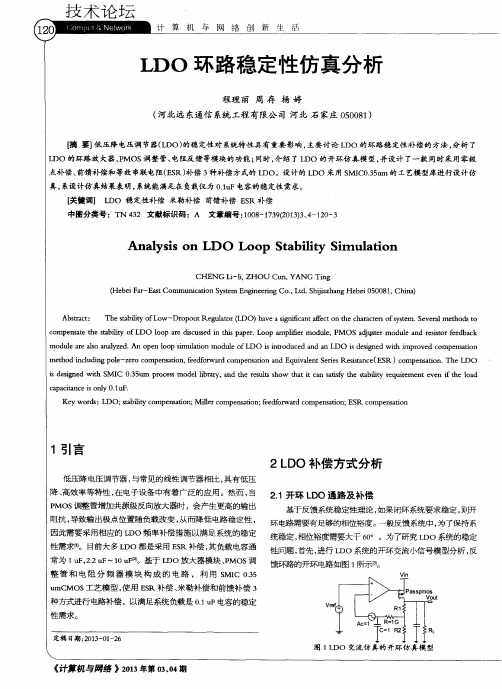
【摘 要】低压 降电压调节器(LD0)的稳 定性对 系统特性具有 重要 影响 ,主要讨论 LDO 的环路稳定性补偿 的方法 ,分析 了 LDO 的环路放 大器、PMOS调整 管、电阻反馈等模块 的功 能;同时 ,介绍 了 LDO 的开环仿 真模 型 ,并设计 了一款 同时采 用零极 点补偿 、前馈补偿和等效 串联 电阻(EsR)补偿 3种补偿方式的 LDO。设计的 LDO 采用 SMIC0.35um 的工艺模型库进行设计仿 真 ,系设计仿真结果表明 ,系统能满足在 负载仅 为 0.1uF电容的稳 定性需求。
【关键词】 LDO 稳定性补偿 米勒补偿 前馈补偿 ESR补偿 中图分类号 :TN 432 文献标识码 :A 文章编号 :1008—1739(2013)3、4—120—3
LDO降压转换器的稳定性分析
,,H2
图6 ESR阻值过高时系统的频率响应
—\。
Ⅵ 、弋 ,“一Ⅲ”
卜:;
l\l
。
守吣n’
\一,
图7 EsR阻值过低时系统的频率响应
图8显示了ESR电阻的典型范围和输出电流 之间的关系。
图5线性瞬态响应 从图4和图5可以看出,当输入电压和负载电 流发生变化时,输出电压只有很小的波动。没有发生 振荡.因此,这个系统是稳定的。
2004年
由【10)、(11)两式可以看出,增大调整管的宽 长比(即增大p)和误差放大器(EA)的跨导函,可显 著提高负载调整率与线性调整率,即提高系统的稳 定性。瞬态响应仿真波形分别如图4、图s所示。
J 85 >
、l 80
。
o
V
l 75
f
1 70
{l \~
寸 王 500
{ J
I 0
1——————巧—————可玎
Time(1in)/u s
图4负载瞬态响应
H >3 50
、
o
3 00
0J
万方数据
i^
1.81
>
j.8
0 180
1.79
0
。l l 1
.
{I
”
100
:l 200
有正确EsR阻值的电容是一件困难的事。对大多数 LD0转换器来说,EsR存在最大值和最小值。超出 一定范围的EsR阻值也会引起环路的不稳定性,如 图6、图7所示。
5提高系统稳定度的方法
反馈系统的稳定性可通过内部或外部的补偿来 实现.内部提高稳定性的方法在前面已有比较详细 的阐述,这里主要讨论外部补偿的方法.
系统必须有足够的相位裕度(>60。),才能保证 稳定。最普遍的做法是在系统中引入一个零点,抵消 由极点引起的相移和增益下降.为了使LDO转换 器正常工作,必须要有输出电容c0。利用输出电容 的寄生等效电阻(EsR)来产生这个零点是最简单、 最便宜的方法。
LDO的选用原则及技术参数及在开关电源中的作用

LDO的选用原则及技术参数及在开关电源中的作用LDO(Low Dropout Regulator)是一种线性稳压器,主要用于在开关电源中提供稳定的低压输出。
LDO的选用原则和技术参数以及在开关电源中的作用如下:一、LDO的选用原则:1.电压稳定性:LDO的输出电压需要保持稳定,不会因输入电压变化或负载变化而产生较大的波动。
2.负载能力:LDO需要具备足够的负载能力,能够在一定范围内承受变化的负载而不引起输出电压波动。
3.降压效率:LDO的降压效率是指输出电压与输入电压之间的差值,效率越高,能量损耗越小。
4.噪声控制:LDO需要具备良好的抑制噪声的能力,以避免对其他电路产生干扰。
5.短路保护和过热保护:LDO需要具备短路保护和过热保护功能,以保护自身和其他器件的安全。
6.封装形式:根据应用环境的要求选择适合的LDO封装形式,例如SOT-23、TO-220等。
二、LDO的技术参数:1.输入电压范围(VIN):LDO的输入电压范围是指能够正常工作的输入电压范围。
2.输出电压(VOUT):LDO输出的稳定电压值,根据应用需求选择合适的输出电压。
3.输出电流(IOUT):LDO能够提供的最大输出电流,需要根据负载要求选择合适的输出电流。
4.静态电流(IQ):当无负载情况下,LDO自身的工作电流。
5.降压效率(η):输出功率与输入功率之比,通常以百分比表示。
6.抑制噪声(PSRR):对输入电压的变化或者噪声对输出电压的抑制能力。
7.脉冲响应:LDO对负载变化的快速响应能力。
8.温度范围:LDO能够正常工作的温度范围。
三、LDO在开关电源中的作用:1.滤波器作用:LDO可以在开关电源输出端提供稳定的滤波电压,用于滤除开关电源产生的高频噪声。
2.稳压作用:LDO可以将开关电源的输出电压稳定在设定的目标电压,保证电路其他部分的正常工作。
3.噪声抑制:LDO能够抑制由开关电源产生的噪声,以减少对系统中其他器件的干扰。
LDO的环路稳定性分析

The Analysis of LDO and the Stability of LoopCompensationXuewen Wang , Fengge Wang , Zhongwei LiInstitute of Microelectronics, School of Information and TechnologyNorthwest UniversityXi’an, ChinaAbstract: This paper discusses loop compensation methods of LDO. We especially analyze the LDO loop op-amp module, PMOS adjustment module, resistor feedback module. Moreover, the zero-pole compensation, feed-forward compensation and ESR compensation are adopted simultaneously to compensate LDO. This article simulates the designed LDO system with the CSMC 0.5um CMOS technical model. The system can meet the stability requirements under the load capacitance of 0.1uF.Keywords: LDO, stability of compensation, Miller compensation, feed-forward compensation, ESR CompensationI.I NTRODUCTIONLow Dropout Voltage Regulator (LDO), compared with the general linear regulators has the characteristics of low dropout and high conversion efficiency. It has a wide range of application prospects in the field of portable electronic products. However, if we add a common-source inverting amplification for PMOS pass element, it will have a high output impedance, which makes the output pole location change with the load and the circuit stability low. So we need the LDO Frequency Compensation loop to meet its requirements of stability strictly. Currently the typical commercial LDO is compensated with ESR and the load capacitance is generally 1uF, 2.2uF to 10uF. Based on the analysis of the op amp LDO module, PMOS adjustment module and resistor feedback module, this article uses ESR compensation, internal Miller compensation and feed-forward compensation these three methods to make the frequency compensation and simulates with the CSMC 0.5um CMOS technical model to meet the stability requirements under the load capacitance of 0.1uF.II.A NALYSIS OF V ARIOUS LDO C OMPENSATIONSA.LDO Open-loop Model DdiagramBased on the stability theory of feedback system if the closed-loop system aims to stabilize the phase of open-loop circuit system changes can not be too large, that is to say, there must be a certain degree of phase margin. Generally the phase margin is greater than 60 degrees to meet industrial applications. Therefore, to study stability problems of LDO system, firstly, we must make an open-loop AC analysis of LDO system, open the loop in the feedback way as is shown inFigure 1.Figure 1. Open-loop Simulation of the LDO AC CircuitIn Figure1, gm1, R1, C1 can be seen as the simplified forms of the small-signal amplifiers. RF1, RF2 are the feedback resistors, the current flows simultaneously through RF1, RF2 is I Q. PASS PMOS is the tube to adjust output. The circuit cuts off the closed AC signals with inductors Lopen and capacitors Copen in the resistor feedback path.The simplified structure ofthe open-loop circuit is shown in Figure 2.2010 International Conference on Electrical and Control EngineeringFigure 2. LDO AC Open-loop Block DiagramH1, H2, H3 represent respectively the transfer functions of error amplifier module, PMOS control module and the feedback resistor. Now each module will be analyzed and compensated separately. B. Compensation of ESR ZeroThe compensation method that almost every single-chip LDO will use is ESR (Equivalent Series Resistance). Zero compensation is the one that mainly aims at adjusting the tube transfer function H2. Considering the ESR, the capacitor can be expressed as a circuit consisting of ESR resistance and capacitor in series, as is shown in Figure 3.Figure 3. The Output Impedance Equivalent Circuit with ESR1//()11()OUT OUT ESR OUTOUT ESROUT OUT OUT ESR Z R R sC sC R R sC R R =++⋅=⋅+⋅+ (1)As can be seen, the AC components of the output impedance not only contain the load pole, but also produce a new ESR zero 1/C OUT *R ESR . If the new ESR zero is in the appropriate frequency range, the loop would be compensated well. However, if the ESR zero frequency is higher than the Unit Gain Frequency (UGF), there is no compensation effect, if the zero is small, as the bandwidth of the zero will increase while it compensates the phase, so increase of the bandwidth would make the phase in the UGF drop more, so that the phase margin is not enough[3].The LDO will normally require the output capacitor ESR value be in a particular range. While designing the compensation, taking into account the fact that the load capacitance has been selected as 0.1uF ceramic capacitor 104,when simulating the circuit, this article selects the ESR value as a typical value 0.2Ω, and the scope of its ESR can vary from 80m Ω to 0.8Ω. The load capacitor value of the commercially available LDO is generally 1uF, 2.2uF to 10uF, so the use of a smaller load capacitance can not only improve the transient response of LDO, but also reduce costs. C. Compensation of Internal Miller ZeroThe general LDO can meet the stability requirements through rigorous ESR compensation, but as for the circuits which require particular capacitors, they may not meet the designing requirements. To reduce the requirements of ESR zero, we can generate the internal zero of LDO to compensate it. One common approach is to control the zero resistance in the process of the two-stage op-amp Miller compensation, so that the zero in the right-half flat can move to the left flat, and thus the phase of the system is compensated. The compensation is for the transfer function H1 of the op amp module.Figure 4. Two-stage Op-amp Structure with A Zero ResistanceThe figure above shows the two-stage op-amp block diagram with a zero resistance. If the zero resistance R C does not exist, then the resulted zero location of the right-half plane is ωZ =gm 2/C C . The zero location with the zero resistance is2112()fz Cc Rc gm π=⋅⋅− (2)When R C =1/gm 2, the zero generated disappears, if R C >1/gm 2, a negative zero can be generated. If R C continues to increase to an appropriate location, it can be used to compensate for the phase by off setting a pole. By adjusting the internal Miller zero, LDO can get a relatively good phase margin. Similar to the ESR zero, this zero value can not be too large or too small, or we can not get the best compensation. Inthis paper, we adjust the phase margin to the best by adjusting the R C in our design.pensation of FeedforwardThe feedforward compensation is also a commonly used compensation method which is mainly for the compensation of the resistance feedback loop transfer function H3, that is to span a feed-forward capacitor between the output signal and the feedback signal, generating zero-pole pairs of the system to compensate for the phase, as shown in Figure 5. According totheir transfer functions, the zero and the pole are [5]:Figure 5. Resistor Feedback Networkwith with A FeedforwardCompensation Capacitor112ZFF FfC Rπ=⋅⋅(3)1212(//)PFF F FfC R Rπ=⋅⋅(4)Formulas(3)and(4)are the zero poles of the transferfunction H3 of the feedback loop, whose zero is always lessthan its pole. The net compensation phase obtained is thedifference between the zero phases increased and the pole phasereduced. In order to improve the phase margin, the best locationof the zero-pole pairs is on the UGF. As can be seen, when R F1is far larger than R F2, the zero poles are far away from eachother to obtain the maximum phase compensation. When R F1 isreduced, the zero poles get close to each other, graduallyreducing the effect of phase compensation. Thus, the higher theratio of R F1/ R F2 is, the greater the feedforward capacitor is, andthe feed-forward compensation will become more effective [5].RF1 and RF2 determine the size of the LDO output voltage,a larger value of the feedback resistance can reduce the LDOquiescent current and improve the efficiency, but the accuracyand matching of too large integrated resistances are poor interritory and craft, thus they can not meet the requirements, soRF1 and RF2 are normally fixed between a few thousand ohmto several hundred thousand ohm. The feedforward capacitorCFF depends on the resistance value.III.LDO C IRCUIT D ESIGN AND S IMULATIONLDO designed in this paper uses three kinds of phasecompensation methods. The circuit structure is shown in Figure6. The op-amp of the circuit uses the NMOS differentialamplifier as the input stage, and the output stage uses thepush-pull output structure (P3, P4, N3, N4, N6 constitute thesame phase amplifier). P0 is the adjustment pipe. Thissimulation circuit cuts the ac loop circuit by inductance in thefeedback path.In the LDO circuit designed in this paper, Cout and Resrconstitute the ESR zero compensation. The load capacitanceCout = 0.1uF, the capacitor equivalent series resistance Resr isthe typical 0.2Ω, Rc and Cc constitute the internal Miller zerocompensation network in op-amp, where Cc=5pF, Rc=11KΩ,CFF and the feedback resistors RF1, RF2 constitute thefeed-forward compensation network, where RF1=RF2=100KΩ,at which time Vout2Vref, supposing the feed-forwardcapacitor CFF=2pF.Figure 6. Open-loop Simulation of LDOThe curve of the LDO Open-loop Simulation is shown inFigure7.The load current is 200mA. When the load is 0.1uF,ESR=0.2, the unit gained bandwidth is 7.2MHz, and the phasemargin is 68 degree. As can be seen in Figure7, the main polein the internal LDO is about 537Hz, the load pole is about 159KHz, the zero of internal Miller compensation is about 2MHz, the ESR zero compensation is about 8MHz. The overall effects of the three kinds of compensations make the LDO still able to meet the stability requirements when the capacitor is as small as 0.1uF, and is better than a part of the research techniques both at home and abroad in the aspects of frequencyand stability.Figure7 LDO Open-loop Frequency Response Simulation WaveformsIV. S UMMARYThis paper mainly analyzes three kinds of LDO stability compensation methods: ESR zero compensation, zero internal Miller compensation, feedforward compensation, and designs a LDO circuit with better stability using these three methods of compensation. At the same time, the circuit uses a CMOS technical model with the CSMC of 0.5um to make a simulation analysis. The simulation results show that when the load capacitor is 0.1uF (ESR=0.2), the open-loop gain of the circuit is 98dB, the bandwidth is 7.2MHz, the phase margin is 68 degree. As long as the ESR range is between 80m Ω to 0.8Ω, they are able to meet the stability requirements of LDO system.R EFERENCES[1] Gabriel Alfonso Riccon-Mora. Current efficient, low coltage, lowdrop-out regulators. In Partial Fulfillment of the Requirements for the Degree of Doctor of Philosophy in Electrical Engineering, Georgia Institute of Techcology. 1996,11.[2] Ramy Tantawy. Performance Evalution of CMOS Low Drop-OutVoltage Regulators. The 47th IEEE International Midwest Symposium on Circuits and Systems. 2004[3] Chester Simpson. Linear Regulators: work principle and itscompensation. The United States National Semiconductor Application Notes. 2000.[4] Phillip E. Allen. FengJun LiZhiqun translate CMOS Analog IC Design(second edition). Electronic Industry Press. 2005. p214.[5] Chester Simpson. Linear regulator to optimize feedforwardcompensation. The United States National Semiconductor Application Notes. 2007.[6] Chaitaanya K. Chava. A Frequency Compersation Scheme for LDOVoltage Regulators. IEEE Transactinons on Circuits and Systems. Vol.51,No.6. June 2004.。
一种无片外电容LDO的稳定性分析
The s t a b i l i t y a na l y s i s o f a n o u t pu t - c a p a c i t o r l e s s LD0
r ANG Z e . z h o u
( C o l l e g e o fS c i e n c e , G u i z h o u U 凡 e 瑙 , G u i y a n g 5 5 0 0 2 5 , C h i n a )
第2 1卷 第 1 6期
V0 1 . 2 1 No . 1 6
电 子 设 计 工 程
E l e c t r o n i c De s i g n En g i n e e r i n g
2 0 1 3年 8月
Aug . 2 01稳 定性 分析
关键词 : L D 0;无 片 外 电容 L D 0; 相 位 裕 度 ;零 极 点 ; 稳 定性 ; 电 流 缓 冲 器 频 率 补 偿 中图 分 类 号 : T N 4 9 5 文 献标 识 码 : A 文 章 编 号 :1 6 7 4 — 6 2 3 6 ( 2 0 1 3 ) 1 6 — 0 1 4 7 — 0 4
c a p a c i t o r l e s s L DO’ S p o l e s a n d z e us i s p r e s e n t e d i n t h i s a r t i c l e .An o u t p u t - c a p a c i t o r l e s s L DO wi h c t u r r e n t b u fe r
LDO稳压器的稳定性分析及在整车上的应用
1LDO 稳压器LDO (Low Dropout voltage)稳压器是近年出现的一类新型电源稳压芯片,各大半导体供应商都有自己的产品,如美国国家半导体公司的LM2951。
在LDO 稳压器中,调整管是单个PNP 管,如图1所示。
LDO 最大的优势是PNP 管在调节输出时仅有很小的压降,满载时压降的典型值小于500mV,轻载时的压降仅有10~200mV。
LDO 的这个低压降特点,特别适用于车辆电压环境。
通常整车的电压环境为9~16V,极端情况下能低至6V,在此种条件下,如果模块采用常规稳压芯片为车辆ECU 提供稳定的5V 电源,几乎就是不可能了。
由此,当今整车上ECU 中的电源部分设计,基本都采用了LDO 芯片进行设计。
稳压器的工作原理:通过连接到误差放大器反向输入端的分压电阻对输出电压进行采样,误差放大器的同相端接到一个参考电压,该参考电压由IC 内部的带隙参考源产生。
误差放大器总是试图迫使两个输入端电压相等,为此,它控制调整管输出足够的负载电流,以保证输出电压稳定:U out =U REF (1+R 1/R 2)。
2LDO 稳压器的稳定性分析及补偿方法任何一个闭环系统都存在环路稳定性问题,作为负反馈系统的LDO 当然也不例外。
这里的稳定性指的是频率稳定性,由于电路中存在有电感电容等元件,在不同的频率下,会产生相应的滞后的或超前的相移,相移条件达到180°,同时幅值足够的条件下,会使负反馈电路变为正反馈电路,此时电路就产生了振荡,输出正弦波。
此时,LDO 就不能发挥电源芯片的作用。
传统的自动控制理论提供了稳定性的判断方法。
图2所示为传统LDO 小信号架构,影响系统稳定性的主要因素有:误差放大器、调整管、反馈电阻网络、输出电容及其等效串联电阻图1LDO 原理图修改稿收稿日期:2013-09-06作者简介:侯利程(1980-),男,硕士研究生,工程师。
LDO 稳压器的稳定性分析及在整车上的应用侯利程,辛长宇,许瑞沁(上海汽车集团股份有限公司乘用车公司技术中心,上海201804)摘要:随着电子模块在整车上的快速增长,传统的电源芯片如LM317等已不能满足需求,而LDO 芯片在模块的电源上得到了广泛的应用。
LDO线性稳压器及其稳定性研究
LDO线性稳压器及其稳定性研究摘的要:低压差(Low Dropout, LDO)线性稳压器具有结构简单、低噪声、低功耗以及小封装和较少的外围应用器件等突出优点,在便携式电子产品中得到广泛的应用。
随着各种便携式电子产品功能的多样化和性能的完善,对作为电源管理的LDO的性能也提出了更高的要求,最基本的,要使LDO高性能的工作,必须要有好的频率响应和好的瞬态响应。
关键词:低压差线性稳压器稳定性研究要使LDO高性能的工作,必须要有好的频率响应和好的瞬态响应。
从频率稳定性考虑,由于片外电容和调整管大的栅电容,导致在单位增益带宽内存在两个极点。
若补偿不当,这两个低频的极点会损害整个电路的稳定性。
再加上各增益级的输出极点,整个系统就更难以稳定。
另外,在输入电压大于输出电压一定数值时,LDO电路系统具有保证输出电压稳定的特点。
但是,如果在输入电压或者是负载电流发生变化时,输出电压值会产生一定的跳变。
输出电压的跳变值将通过芯片内部的反馈网络送到误差运算放大器的输入端,放大器输出电压控制输出调整管以稳定输出电压。
如果不采用任何频率补偿,系统必将处于不稳定状态。
因此,LDO 的稳定性问题,可以归结为误差放大器的频率补偿问题。
一、LDO 的稳定性国内外一直都非常重视对频率补偿问题的研究,也提出了多种适合不同条件的补偿方案,并不断对原来的方案进行改进和发展。
1、简单米勒补偿用于两级放大器的简单米勒补偿应该算是最简单的频率补偿方法。
它利用米勒效应将两个相近的极点分裂,一个推向高频,一个推向低频,这样就使放大器达到合适的相位裕度。
其拓扑和频率响应如图1所示。
只要选择合适的补偿电容Cm 就可以即达到所需相位裕度,稳定系统,又不会过分减小带宽。
2、嵌套米勒补偿以上是两级运放的主要频率补偿方案,但是随着对一些性能要求的提高,需要提高运放增益,这样就要求再增加增益级。
LDO其实至少为三级,调整管是输出级,而且为了达到更好的瞬态响应和频率稳定性,往往需要在误差放大器和调整馆之间增加一个缓冲级,这样不仅提高放大器的驱动能力,而且由于缓冲级的低输出阻抗,可以将调整管栅端产生的极点调到频率稍高的地方,有助于达到更好的稳定性。
设计LDO不得不考虑的因素集锦
设计LDO不得不考虑的因素集锦1.稳定性:稳定性是LDO的核心指标之一、一个好的LDO必须能够在负载变化、温度变化和输入电压变化的情况下保持输出电压的稳定性。
稳定性的设计考虑包括负载传导率、补偿网络和保护电路等。
2.压降:LDO的目标是在输入和输出之间提供一个稳定的电压差,因此,设计时需要考虑LDO的输出压降特性。
这涉及到输入电压范围、输出电流能力、线性调整范围和功耗等因素。
3.噪声:噪声是一个重要的设计指标,尤其是对于要求高精度的应用场景。
设计时需要考虑输入端的噪声滤波和输出端的噪声抑制,以确保LDO能够提供干净的电源。
4.效率:效率是评估LDO性能的指标之一、设计时需要考虑输入输出差压、电源电流和负载电流等参数,以最大化LDO的效率。
5.温度:温度是影响LDO性能的重要因素之一、设计时需要考虑LDO 的温度特性,以确保在不同温度下都能提供稳定的输出。
6.线性度:线性度是衡量LDO稳定性的重要指标。
设计时需考虑输入输出差压、输出动态响应和输出漂移等参数,以确保LDO提供高线性度和良好的动态响应。
7.过载保护:过载保护功能是LDO设计不可或缺的一部分。
设计考虑包括过流保护、过热保护和短路保护等。
8.抗干扰能力:抗干扰能力是LDO设计中要考虑的重要因素之一、设计时需要考虑输入端和输出端的滤波能力,以减少来自外部环境的干扰。
9.外部元件:设计LDO时还需要考虑外部元件的选择和连接方式。
这包括输入和输出电容、电感和电源滤波器等。
10.尺寸和封装:根据应用的需求,设计时需要考虑LDO的尺寸和封装形式。
这涉及到PCB设计和系统集成。
以上仅是设计LDO时需要考虑的一些基本因素,实际设计还需要根据具体应用场景和要求进行深入分析和优化。
设计人员需要仔细权衡各种设计参数,并做出适当的选择,以实现最佳性能和稳定性。
- 1、下载文档前请自行甄别文档内容的完整性,平台不提供额外的编辑、内容补充、找答案等附加服务。
- 2、"仅部分预览"的文档,不可在线预览部分如存在完整性等问题,可反馈申请退款(可完整预览的文档不适用该条件!)。
- 3、如文档侵犯您的权益,请联系客服反馈,我们会尽快为您处理(人工客服工作时间:9:00-18:30)。
(1)提高误差放大器的增益;(2)提高基准电压的精度;(3)匹配反馈电阻;(4)在不增加过多成本的前提下适当增加器件尺寸或采用共源共栅结构。
§2.2 负载瞬态响应分析随着各类低压、大负载、高速数字电路的高速发展,我们所设计的LDO 也需要适应客户的应用需要,响应速度更加快速化。
对于数字应用的环境,由于数字电路开关转换,供电的电源就会经常发生负载阶跃变化,负载的快速变化会使稳压器输出产生一个瞬态脉冲,这对大部分数字电路来说是较难接受的,因此降低LDO 线性稳压器的负载瞬态响应脉冲,提高瞬态响应速度是非常重要的和关键的。
图2.1给出了LDO 负载瞬态响应的典型波形图[6]。
表征瞬态响应时间的为Δt 1和Δt 3,Δt 2和Δt 4则表征建立时间。
Δt 1表示为: sr pass sr I V C t ∆+=+≈∆c1c11BW 1BW 1t (2-7) 其中,BW cl 为系统的闭环带宽,C pass 为传输管的栅极寄生电容,t sr 和I sr 分别为传输管栅极驱动信号的压摆时间和压摆限制电流,ΔV 为输出电压变化值。
Δt 3同样反比于系统的闭环带宽,但它不受压摆电流的限制。
为了减小Δt 1和Δt 3,需要增加系统的带宽和驱动栅极的压摆电流。
建立时间Δt 2由开环频率响应的相位裕度决定,Δt 4由反馈电阻的电流决定。
当输出负载阶跃变化时,传统稳压器输出会产生上冲和下冲,该上冲和下冲一方面可以代表负载瞬态响应的速度,同时直接影响输出电压的精度。
当输出电流从0跳变到最大输出电流I O(MAX),那么输出最大下降脉冲值ΔV TR :ESR MAX O OUTMAX O ESR OUT MAX O TR R I t C I V t C I V )(1)(1)(+∆=∆+∆=∆ (2-8) 由式(2-8)可以看出,影响下冲的因素主要是输出电容值、最大负载电流值、瞬态响应的时间和输出电容的等效串联电阻值。
在LDO 线性稳压器中,主要由系统的闭环带宽、输出电容值、输出电容的等效串联电阻(ESR)和负载电流这几个因素决定由负载电流突然变化引起输出电压的响应时间。
下面对LDO 的稳定性、输出电压精度、静态电流和负载瞬态响应速度的关系进行分析。
LDO 的稳定性受到相位裕度的影响,高增益和宽带宽会削弱环路得稳定性,而快速负载瞬态响应则要求宽的带宽,因此环路稳定性与负载瞬图2.1 LDO 负载瞬态响应典型波形态响应是矛盾的关系。
环路稳定性与输出电容及等效串联电阻有直接关系,输出电容与输出阻抗形成一个极点,在小负载应用中一般为主极点,输出电容等效串联电阻与输出电容形成的ESR零点也会影响到环路的稳定性。
在采用小ESR陶瓷电容时,该零点会远离单位增益带宽,对稳定性影响变小。
大输出电容会将输出极点推向原点,减小环路的带宽,提高环路稳定性,但这也减小了负载瞬态响应的速度。
而输出精度要求小的ΔV TR,这就要求大的输出电容,这也减小了环路负载瞬态响应的速度,因此输出精度与负载瞬态响应也是矛盾的关系。
而且静态电流必然导致压摆电流的减小,进而缩小了瞬态响应的速度。
因此,在获得低静态电流的同时必然会衰减负载瞬态响应速度。
提高瞬态响应的方法一般是通过增加静态电流来实现;或者是采用双环路结构,通过增加一个快速响应的前馈通路来实现[14]。
这两种结构往往是以牺牲效率为代价而且取得稳定性的电路也很复杂。
还有一种方法是通过增加buffer来提高瞬态响应速度。
buffer结构通常是一个源极跟随器[15],但这种结构会减小功率管栅极的共模驱动范围因此减小了信噪比。
为了能够获得足够大的负载范围,buffer级一般需要轨对轨的运算放大器实现,这就增加了系统的电路难度与复杂度。
还有一种方法就是增加一个作为单位增益配置的非buffer结构的运算放大器,这个单位增益配置的buffer的输出阻抗就可以是运算放大器输出阻抗除以环路的增益,这样小的输出阻抗就会在功率管栅极产生小的时间常数,可以保证功率管栅极快速充放电,完成快速响应[16]。
综合以上的分析可以得出,负载瞬态响应需要折中环路稳定性、输出电压精度和静态电流,在获得快速负载瞬态响应的同时要达到高输出精度和低静态电流是很艰巨的任务。
§2.3 稳定性分析2.3.1 传统LDO稳压器的稳定性分析及补偿方法任何一个闭环系统都存在环路稳定性问题,作为负反馈系统的LDO当然也不例外。
图2.2所示为传统LDO小信号架构,影响系统稳定性的主要因素有:误差放大器、调整管、反馈电阻网络、输出电容及其等效串联电阻(ESR)、输出负载、旁路电容等。
由于该LDO的架构可以看成两级运放的架构,我们计算开环增益为[17]:R L 图2.2 LDO稳压器的典型结构o mp o m F F F v v F F F REF FB REF FB v Z g Z g R R R A A R R R V V V V V V A 1121221212out out +=+=⨯== (2-9) 其中g m1为误差放大器的跨导,Z o1为误差放大器的输出阻抗,g mp 为调整管的跨导,Z o 为输出级的输出阻抗。
11111111//C SR R SC R Z o +== (2-10) R 1和C 1分别为误差放大器输出端的等效电阻和寄生电容。
L L ESR o R SC R Z Z //)1//(2o += (2-11) Z o2为输出级向LDO 内部看进去的输出阻抗,该阻抗可以表示为功率管输出阻抗R o_pass 与反馈电阻的并联:)//(21pass _o2F F o R R R Z += (2-12)由于R o_pass 远小于反馈,因此pass _o2o R Z ≈。
综合式(2-10)、(2-11)代入(2-12)整理得:SCR R SC R R R Z L ESR L ESR L pass o )(1)1(//_o +++= (2-13) 因此产生的零极点分别为:L L Mpass o C R R p )//(21_1π= (2-14)11221R C p π=(2-15) ESRL R C z π211= (2-16) 图2.3给出了LDO 稳压器系统典型的频率响应曲线,极点P b 由输出级寄生电容C b 产生,其表达式可以表示为:b ESR b ESR ds b C R C R R P ππ21)||(21≈= (2-17) 由于较小的等效串联电阻和寄生电容,该极点一般都远离单位增益带宽,对环路稳定性没有太大的影响。
从负反馈系统理论可以得出,如果一个系统中存在两个极点和一个零点,零点可以补偿其中的一个极点,这个系统就是稳定的系统。
因此,采用输出电容ESR 产生的零点补偿内部的极点成了一段时间内LDO 的补偿方法[18]。
由于使用该补偿方法需要图2.3 LDO 稳压器的频率响应输出电容的ESR 必须在我们所需要的电阻范围内,因此对使用的输出电容有更高的要求[18]。
因此,具有稳定ESR 值且适合我们使用的就是钽电容。
但是,随着LDO 向低成本和小尺寸的发展,这种补偿方法逐渐被淘汰,取而代之的是Miller 补偿[19],[20],[21]。
图2.4所示为传统的快速负载瞬态响应LDO 的Miller 补偿方式小信号分析图。
图中的R C 、C C 分别为调零电阻和Miller 电容,在不考虑输出电容等效串联电阻产生的零点的情况下,系统的传输函数如下:)/1)(/1()/1()(2110p p z s s s A s H ωωω+++= (2-18) ))//(//(A 2121210F F L O O m m R R R R R g g += (2-19)CO O m p C R R g 21211=ω (2-20) L m p C g 22=ω (2-21) )/1(121C m c z R g C -=ω (2-22) 单位增益带宽 c m C g GBW 1=(2-23) 为保证系统稳定,必须保证ωp2>>ωp1,但是,当负载电流增大时,第二级的增益g m2R o 降低,密勒效应减弱,ωp1向ωp2靠近,系统容易出现不稳定。
为了保证大负载下的稳定,C c 需要加大,这将导致系统带宽的降低同时导致芯片面积的增加,同时导致系统的负载瞬态响应的降低。
随着补偿技术的发展,随后出现的动态补偿技术[22],[23]和最近提出的自适应L图2.4传统快速负载瞬态LDO 补偿方式Miller 补偿技术[22]-[25]克服了不同负载应用下的环路的稳定性问题,而且取得了很好的效果,而且对300mA 左右的中等负载应用场合效果明显。
但是此种补偿方式使得负载瞬态响应变差,低压大负载应用中该自适应补偿零点会消失,无法保证系统的稳定。
因此,我们需要一种新型结构的LDO 来解决大负载、低电源应用下LDO 的稳定和快速响应。
2.3.2 XD0117补偿方案针对高精度、大负载、快速负载瞬态响应应用的数字系统,这就要求所设计的LDO 要有高增益、宽带宽。
对误差放大器而言,高的增益更加容易导致环路的不稳定,大负载应用会导致环路输出极点的大范围变化,这又加剧了环路的不稳定性。
同时大负载意味着需要更多的功率管来提供负载电流,大量的功率管就会导致其栅极寄生电容加大。
因此误差放大器输出级的高阻抗点与功率管栅极大的寄生电容必然会产生低频的极点。
而前面所述的无论是ESR 补偿还是传统的Miller 补偿还是现如今提到的自适应补偿,在大负载、快速负载瞬态响应、需要高精度输出和低成本制约的情况下都没法保证环路的稳定性。
高增益的获得通常是通过共源共栅或者通过反馈增大输出阻抗获得的,然而高的输出阻抗与大的寄生电容很容易产生低频的极点,这对于环路稳定性和宽带宽的获得是不利的。
当然,我们也可以通过增加环路的跨导来增加增益,以PMOS 器件为例,跨导表达式如下:D mp I LW g ox p C 2μ= (2-24) μp 与C ox 都是由工艺本身决定的。
为了获得大的跨导,我们可以增加器件的宽长比或者增加电流,前者会增加芯片的面积,增加设计的成本;后者会增加芯片的功耗。
因此跨导的增加需要折中成本与功耗的矛盾。
XD0117的误差放大器采用电流镜作为架构会合理地避开高阻点,将误差放大器输出级产生的寄生极点推向高频,使整个系统成为仅仅由输出极点控制的单极点系统,保证了环路的稳定性。
通过高跨导获得的高增益取得了好的输出精度,同时也拓宽了系统的带宽,提高了负载瞬态响应的速度,电流镜本身的低阻抗和大电流也将减轻负载瞬态响应影响因素中的压摆限制电流的影响,使瞬态响应更好。
图2.5所示为XD0117采用的新颖的LDO 结构的小信号分析图。