2Radiative heat transfer between nanostructurespdf
FRET 维基百科
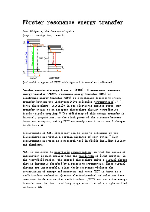
Förster resonance energy transferFrom Wikipedia, the free encyclopediaJump to: navigation, searchJablonski diagram of FRET with typical timescales indicatedFörster resonance energy transfer (FRET), fluorescence resonance energy transfer (FRET), resonance energy transfer (RET) orelectronic energy transfer (EET) is a mechanism describing energy transfer between two light-sensitive molecules (chromophores).[1] A donor chromophore, initially in its electronic excited state, may transfer energy to an acceptor chromophore through nonradiative dipole–dipole coupling.[2] The efficiency of this energy transfer is inversely proportional to the sixth power of the distance between donor and acceptor, making FRET extremely sensitive to small changes in distance.[3]Measurements of FRET efficiency can be used to determine if two fluorophores are within a certain distance of each other.[4] Such measurements are used as a research tool in fields including biology and chemistry.FRET is analogous to near-field communication, in that the radius of interaction is much smaller than the wavelength of light emitted. In the near-field region, the excited chromophore emits a virtual photon that is instantly absorbed by a receiving chromophore. These virtual photons are undetectable, since their existence violates the conservation of energy and momentum, and hence FRET is known as a radiationless mechanism. Quantum electrodynamical calculations have been used to determine that radiationless (FRET) and radiative energy transfer are the short- and long-range asymptotes of a single unified mechanism.[5][6]Contents[hide]∙ 1 Terminology∙ 2 Theoretical basis∙ 3 Experimental co nfirmation of the Förster resonance energy transfer theory∙ 4 Methods to measure FRET efficiencyo 4.1 Sensitized emissiono 4.2 Photobleaching FRETo 4.3 Lifetime measurements∙ 5 Fluorophores used for FRETo 5.1 CFP-YFP pairso 5.2 BRETo 5.3 Homo-FRET∙ 6 Applicationso 6.1 Biology∙7 Other methods∙8 See also∙9 References∙10 External linksTerminology[edit]Förster resonance energy transfer is named after the German scientist Theodor Förster.[7] When both chromophores are fluorescent, the term "fluorescence resonance energy transfer" is often used instead, although the energy is not actually transferred by fluorescence.[8][9]In order to avoid an erroneous interpretation of the phenomenon that is always a nonradiative transfer of energy (even when occurring between two fluorescent chromophores), the name "Förster resonance energy transfer" is preferred to "fluorescence resonance energy transfer;" however, the latter enjoys common usage in scientific literature.[10] It should also be noted that FRET is not restricted to fluorescence. It can occur in connection with phosphorescence as well.[8]Theoretical basis[edit]The FRET efficiency () is the quantum yield of the energy transfer transition, i.e. the fraction of energy transfer event occurring per donor excitation event:[11]where is the rate of energy transfer, the radiative decayrate, and the 's are the rate constants of any other de-excitation pathways.[12]The FRET efficiency depends on many physical parameters that can be grouped as follows:∙The distance between the donor and the acceptor (typically in the range of 1-10 nm)∙The spectral overlap of the donor emission spectrum and the acceptor absorption spectrum.∙The relative orientation of the donor emission dipole moment and the acceptor absorption dipole moment.depends on the donor-to-acceptor separation distance with an inverse 6th power law due to the dipole-dipole coupling mechanism:with being the Förster distance of this pair of donor andacceptor, i.e. the distance at which the energy transfer efficiency is 50%.[12]The Förster distance depends on the overlap integral of the donor emission spectrum with the acceptor absorption spectrum and their mutual molecular orientation as expressed by the following equation.[13][14]where is the fluorescence quantum yield of the donor in the absence of the acceptor, κ2 is the dipole orientation factor, is the refractive index of the medium, is Avogadro's number, and is the spectral overlap integral calculated aswhere is the normalized donor emission spectrum, and is the acceptor molar extinction coefficient.[15] The orientation factor κ is given by,Where denotes the normalized transition dipole moment of therespective fluorophore and denotes the normalized inter-fluorophore displacement. κ2 =2/3 is often assumed. This value is obtained when both dyes are freely rotating and can be considered to beisotropically oriented during the excited state lifetime. If either dye is fixed or not free to rotate, then κ2 =2/3 will not be a valid assumption. In most cases, however, even modest reorientation of the dyes results in enough orientational averaging that κ2 = 2/3 doesnot result in a large error in the estimated energy transfer distance due to the sixth power dependence of R0 on κ2. Even when κ2 is quite different from 2/3 the error can be associated with a shift in R0 and thus determinations of changes in relative distance for a particular system are still valid. Fluorescent proteins do not reorient on a timescale that is faster than their fluorescence lifetime. In this case 0 ≤ κ2≤ 4.[15]The FRET efficiency relates to the quantum yield and the fluorescence lifetime of the donor molecule as follows:[16]where and are the donor fluorescence lifetimes in the presenceand absence of an acceptor, respectively, or aswhere and are the donor fluorescence intensities with and without an acceptor, respectively.Experimental confirmation of the Förster resonance energy transfer theory[edit]The inverse sixth-power distance dependence of Förster resonance energy transfer was experimentally confirmed by Wilchek, Edelhoch and Brand[17][18] using tryptophyl peptides. Stryer, Haugland and Yguerabide[19] also experimentally demonstrated the theoretical dependence ofFörster resonance ene rgy transfer on the overlap integral by using a fused indolosteroid as a donor and a ketone as an acceptor. However, a lot of contradictions of special experiments with the theory was oserved. The reason is that the theory has approximate character and gives overstimated distances of 50-100 Angstrems (Vekshin N.L. Energy Transfer in Macromolecules, SPIE, 1997; Vekshin N.L. Photonics of Biopolymers, Springer, 2002).Methods to measure FRET efficiency[edit]In fluorescence microscopy, fluorescence confocal laser scanning microscopy, as well as in molecular biology, FRET is a useful tool to quantify molecular dynamics in biophysics and biochemistry, such as protein-protein interactions, protein–DNA interactions, and protein conformational changes. For monitoring the complex formation between two molecules, one of them is labeled with a donor and the other with an acceptor. The FRET efficiency is measured and used to identify interactions between the labeled complexes. There are several ways of measuring the FRET efficiency by monitoring changes in the fluorescence emitted by the donor or the acceptor.[20]Sensitized emission[edit]One method of measuring FRET efficiency is to measure the variationin acceptor emission intensity.[14] When the donor and acceptor are in proximity (1–10 nm) due to the interaction of the two molecules, the acceptor emission will increase because of the intermolecularFRET from the donor to the acceptor. For monitoring protein conformational changes, the target protein is labeled with a donor and an acceptor at two loci. When a twist or bend of the protein brings the change in the distance or relative orientation of the donor and acceptor, FRET change is observed. If a molecular interaction or a protein conformational change is dependent on ligand binding, this FRET technique is applicable to fluorescent indicators for the ligand detection.Photobleaching FRET[edit]FRET efficiencies can also be inferred from the photobleaching rates of the donor in the presence and absence of an acceptor.[14] This method can be performed on most fluorescence microscopes; one simply shines the excitation light (of a frequency that will excite the donor but not the acceptor significantly) on specimens with and without the acceptor fluorophore and monitors the donor fluorescence (typically separated from acceptor fluorescence using a bandpass filter) over time. The timescale is that of photobleaching, which is seconds to minutes, with fluorescence in each curve being given bywhere is the photobleaching decay time constant and depends on whether the acceptor is present or not. Since photobleaching consists in the permanent inactivation of excited fluorophores, resonance energy transfer from an excited donor to an acceptor fluorophore prevents the photobleaching of that donor fluorophore, and thus high FRET efficiency leads to a longer photobleaching decay time constant:where and are the photobleaching decay time constants of thedonor in the presence and in the absence of the acceptor, respectively. (Notice that the fraction is the reciprocal of that used for lifetime measurements).This technique was introduced by Jovin in 1989.[21] Its use of anentire curve of points to extract the time constants can give it accuracy advantages over the other methods. Also, the fact that time measurements are over seconds rather than nanoseconds makes it easierthan fluorescence lifetime measurements, and because photobleaching decay rates do not generally depend on donor concentration (unless acceptor saturation is an issue), the careful control of concentrations needed for intensity measurements is not needed. It is, however, important to keep the illumination the same for the with- and without-acceptor measurements, as photobleaching increases markedly with more intense incident light.Lifetime measurements[edit]FRET efficiency can also be determined from the change in the fluorescence lifetime of the donor.[14] The lifetime of the donor will decrease in the presence of the acceptor. Lifetime measurements of FRET are used in Fluorescence-lifetime imaging microscopy.Fluorophores used for FRET[edit]If the linker is intact, excitation at the absorbance wavelength of CFP (414nm) causes emission by YFP (525nm) due to FRET. If the linker is cleaved by a protease, FRET is abolished and emission is at the CFP wavelength (475nm).CFP-YFP pairs[edit]One common pair fluorophores for biological use is a cyan fluorescent protein (CFP) – yellow fluorescent protein (YFP) pair.[22] Both are color variants of green fluorescent protein (GFP). Labeling with organic fluorescent dyes requires purification, chemical modification, and intracellular injection of a host protein. GFP variants can be attached to a host protein by genetic engineering which can be more convenient. Additionally, a fusion of CFP and YFP linked by a protease cleavage sequence can be used as a cleavage assay.[23]BRET[edit]A limitation of FRET is the requirement for external illumination to initiate the fluorescence transfer, which can lead to background noise in the results from direct excitation of the acceptor or to photobleaching. To avoid this drawback, Bioluminescence Resonance Energy Transfer (or BRET) has been developed.[24] This technique uses a bioluminescent luciferase (typically the luciferase from Renilla reniformis) rather than CFP to produce an initial photon emission compatible with YFP.Homo-FRET[edit]In general, "FRET" refers to situations where the donor and acceptor proteins (or "fluorophores") are of two different types. In many biological situations, however, researchers might need to examine the interactions between two, or more, proteins of the same type—or indeed the same protein with itself, for example if the protein folds or forms part of a polymer chain of proteins[25] or for other questions of quantification in biological cells.[26]Obviously, spectral differences will not be the tool used to detect and measure FRET, as both the acceptor and donor protein emit light with the same wavelengths. Yet researchers can detect differences in the polarisation between the light which excites the fluorophores andthe light which is emitted, in a technique called FRET anisotropy imaging; the level of quantified anisotropy (difference in polarisation between the excitation and emission beams) then becomes an indicative guide to how many FRET events have happened.[27]Applications[edit]Biology[edit]FRET has been used to measure distance and detect molecular interactions in a number of systems and has applications in biology and chemistry.[28] FRET can be used to measure distances between domains in a single protein and therefore to provide information about protein conformation.[29] FRET can also detect interaction between proteins.[30] Applied in vivo, FRET has been used to detect the location and interactions of genes and cellular structures including intergrins and membrane proteins.[31] FRET can be used to obtain information about metabolic or signaling pathways.[32] FRET is also used to study lipid rafts in cell membranes.[33]FRET and BRET are also the common tools in the study of biochemical reaction kinetics and molecular motors.The applications of Fluorescence Resonance Energy Transfer (FRET) have expanded tremendously in the last 25 years, and the technique has become a staple technique in many biological and biophysical fields. FRET can be used as spectroscopic ruler in various areas such as structural elucidation of biological molecules and their interactions in vitro assays, in vivo monitoring in cellular research, nucleic acid analysis, signal transduction, light harvesting and metallic nanomaterial etc. Based on the mechanism of FRET a variety of novel chemical sensors and biosensors have been developed.[34]Other methods[edit]A different, but related, mechanism is Dexter Electron Transfer.An alternative method to detecting protein–protein proximity is the bimolecular fluorescence complementation (BiFC) where two halves of a YFP are fused to a protein. When these two halves meet they form a fluorophore after about 60 s – 1 hr.[35]See also[edit]∙Förster coupling∙Surface energy transfer∙Dexter electron transfer∙Time-resolved fluorescence energy transferReferences[edit]1.Jump up ^ Cheng, Ping-Chin (2006). "The Contrast Formation in OpticalMicroscopy". In Pawley, James B. Handbook Of Biological Confocal Microscopy(3rd ed.). New York, NY: Springer. pp. 162–206. doi:10.1007/978-0-387-45524-2_8. ISBN 978-0-387-25921-5.2.Jump up ^ Helms, Volkhard (2008). "Fluorescence Resonance Energy Transfer".Principles of Computational Cell Biology. Weinheim: Wiley-VCH. p. 202.ISBN 978-3-527-31555-0.3.Jump up ^ Harris, Daniel C. (2010). "Applications of Spectrophotometry".Quantitative Chemical Analysis (8th ed.). New York: W. H. Freeman and Co.pp. 419–44. ISBN 978-1-4292-1815-3.4.Jump up ^ Zheng, Jie (2006). "Spectroscopy-Based Quantitative FluorescenceResonance Energy Transfer Analysis". In Stockand, James D.; Shapiro, MarkS. Ion Channels: Methods and Protocols. Methods in Molecular Biology,Volume 337. Totowa, NJ: Humana Press. pp. 65–77. doi:10.1385/1-59745-095-2:65. ISBN 978-1-59745-095-9.5.Jump up ^ Andrews, David L. (1989). "A unified theory of radiative andradiationless molecular energy transfer". Chemical Physics135 (2): 195–201. Bibcode:1989CP....135..195A. doi:10.1016/0301-0104(89)87019-3.6.Jump up ^ Andrews, David L; Bradshaw, David S (2004). "Virtual photons,dipole fields and energy transfer: A quantum electrodynamical approach".European Journal of Physics25 (6): 845. doi:10.1088/0143-0807/25/6/017.7.Jump up ^Förster, Theodor (1948). "Zwischenmolekulare Energiewanderung undFluoreszenz" [Intermolecular energy migration and fluorescence]. Annalender Physik (in German) 437: 55–75. Bibcode:1948AnP...437...55F.doi:10.1002/andp.19484370105.8.^ Jump up to: a b Valeur, Bernard; Berberan-Santos, Mario (2012). "ExcitationEnergy Transfer". Molecular Fluorescence: Principles and Applications, 2nded. Weinheim: Wiley-VCH. pp. 213–261. doi:10.1002/9783527650002.ch8.ISBN 9783527328376.9.Jump up ^ FRET microscopy tutorial from Olympus10.Jump up ^Glossary of Terms Used in Photochemistry (3rd ed.). IUPAC. 2007.p. 340.11.Jump up ^ Moens, Pierre. "Fluorescence Resonance Energy Transferspectroscopy". Retrieved July 14, 2012.12.^ Jump up to: a b Schaufele, Fred; Demarco, Ignacio; Day, Richard N. (2005)."FRET Imaging in the Wide-Field Microscope". In Periasamy, Ammasi; Day, Richard. Molecular Imaging: FRET Microscopy and Spectroscopy. Oxford:Oxford University Press. pp. 72–94. doi:10.1016/B978-019517720-6.50013-4.ISBN 978-0-19-517720-6.13.Jump up ^Förster, Th. (1965). "Delocalized Excitation and ExcitationTransfer". In Sinanoglu, Oktay. Modern Quantum Chemistry. IstanbulLectures. Part III: Action of Light and Organic Crystals3. New York and London: Academic Press. pp. 93–137. Retrieved 2011-06-22.14.^ Jump up to: a b c d Clegg, Robert (2009). "Förster resonance energytransfer—FRET: what is it, why do it, and how it's done". In Gadella,Theodorus W. J. FRET and FLIM Techniques. Laboratory Techniques inBiochemistry and Molecular Biology, Volume 33. Elsevier. pp. 1–57.doi:10.1016/S0075-7535(08)00001-6. ISBN 978-0-08-054958-3.15.^ Jump up to: a b Demchenko, Alexander P. (2008). "Fluorescence DetectionTechniques". Introduction to Fluorescence Sensing. Dordrecht: Springer.pp. 65–118. doi:10.1007/978-1-4020-9003-5_3. ISBN 978-1-4020-9002-8. 16.Jump up ^ Majoul, Irina; Jia, Yiwei; Duden, Rainer (2006). "PracticalFluorescence Resonance Energy Transfer or Molecular Nanobioscopy of Living Cells". In Pawley, James B. Handbook Of Biological Confocal Microscopy (3rd ed.). New York, NY: Springer. pp. 788–808. doi:10.1007/978-0-387-45524-2_45. ISBN 978-0-387-25921-5.17.Jump up ^ Template:ISRAEL JOURNAL OF CHEMISTRY. Vol. 1. No. Sa. 196318.Jump up ^ {Edelhoch, H., Brand, L., Wilchek, M. (1967). "Fluorescencestudies with tryptophyl peptides". Biochemistry 6 (2): 547–559.doi:10.1021/bi00854a024. PMID 6047638}19.Jump up ^ Lakowicz, Joseph R., ed. (1991). Principles. New York: PlenumPress. p. 172. ISBN 978-0-306-43875-2.20.Jump up ^ "Fluorescence Resonance Energy Transfer Protocol". WellcomeTrust. Retrieved 24 June 2012.[dead link]21.Jump up ^Szöllősi, János; Alexander, Denis R. (2007). "The Application ofFluorescence Resonance Energy Transfer to the Investigation ofPhosphatases". In Klumpp, Susanne; Krieglstein, Josef. ProteinPhosphatases. Methods in Enzymology, Volume 366. Amsterdam: Elsevier.pp. 203–24. doi:10.1016/S0076-6879(03)66017-9. ISBN 978-0-12-182269-9. 22.Jump up ^ Periasamy, Ammasi (July 2001). "Fluorescence resonance energytransfer microscopy: a mini review". Journal of Biomedical Optics6 (3): 287–291. Bibcode:2001JBO.....6..287P. doi:10.1117/1.1383063.PMID 11516318.23.Jump up ^ Nguyen, AW; Daugherty, PS (March 2005). "Evolutionaryoptimization of fluorescent proteins for intracellular FRET.". Naturebiotechnology23 (3): 355–60. doi:10.1038/nbt1066. PMID 15696158.24.Jump up ^ Bevan, Nicola; Rees, Stephen (2006). "Pharmaceutical Applicationsof GFP and RCFP". In Chalfie, Martin; Kain, Steven R. Green FluorescentProtein: Properties, Applications and Protocols. Methods of Biochemical Analysis, Volume 47 (2nd ed.). Hoboken, NJ: John Wiley & Sons. pp. 361–90. doi:10.1002/0471739499.ch16. ISBN 978-0-471-73682-0.25.Jump up ^ Gautier, I.; Tramier, M.; Durieux, C.; Coppey, J.; Pansu, R.B.;Nicolas, J.-C.; Kemnitz, K.; Coppey-Moisan, M. (2001). "Homo-FRETMicroscopy in Living Cells to Measure Monomer-Dimer Transition of GFP-Tagged Proteins". Biophysical Journal80 (6): 3000–8.Bibcode:2001BpJ....80.3000G. doi:10.1016/S0006-3495(01)76265-0.PMC 1301483. PMID 11371472.26.Jump up ^ Bader, Arjen N.; Hofman, Erik G.; Voortman, Jarno; Van Bergen EnHenegouwen, Paul M.P.; Gerritsen, Hans C. (2009). "Homo-FRET ImagingEnables Quantification of Protein Cluster Sizes with SubcellularResolution". Biophysical Journal97 (9): 2613–22.Bibcode:2009BpJ....97.2613B. doi:10.1016/j.bpj.2009.07.059. PMC 2770629.PMID 19883605.27.Jump up ^ Gradinaru, Claudiu C.; Marushchak, Denys O.; Samim, Masood;Krull, Ulrich J. (2010). "Fluorescence anisotropy: From single molecules to live cells". The Analyst135 (3): 452–9. Bibcode:2010Ana...135..452G.doi:10.1039/b920242k. PMID 20174695.28.Jump up ^ Lakowicz, Joseph R. (1999). Principles of fluorescencespectroscopy (2nd ed.). New York, NY: Kluwer Acad./Plenum Publ. pp. 374–443. ISBN 978-0-306-46093-7.29.Jump up ^ Truong, Kevin; Ikura, Mitsuhiko (2001). "The use of FRET imagingmicroscopy to detect protein–protein interactions and proteinconformational changes in vivo". Current Opinion in Structural Biology11(5): 573–8. doi:10.1016/S0959-440X(00)00249-9. PMID 11785758.30.Jump up ^ Pollok, B; Heim, R (1999). "Using GFP in FRET-basedapplications". Trends in Cell Biology9 (2): 57–60. doi:10.1016/S0962-8924(98)01434-2. PMID 10087619.31.Jump up ^ Sekar, R. B.; Periasamy, A (2003). "Fluorescence resonance energytransfer (FRET) microscopy imaging of live cell protein localizations". The Journal of Cell Biology160 (5): 629–33. doi:10.1083/jcb.200210140.PMC 2173363. PMID 12615908.32.Jump up ^ Ni, Qiang; Zhang, Jin (2010). "Dynamic Visualization of CellularSignaling". In Endo, Isao; Nagamune, Teruyuki. Nano/Micro Biotechnology.Advances in Biochemical Engineering/Biotechnology, Volume 119. Springer.pp. 79–97. Bibcode:2010nmb..book...79N. doi:10.1007/10_2008_48.ISBN 978-3-642-14946-7. PMID 19499207.33.Jump up ^ Silvius, John R.; Nabi, Ivan Robert (2006). "Fluorescence-quenching and resonance energy transfer studies of lipid microdomains in model and biological membranes (Review)". Molecular Membrane Biology23(1): 5–16. doi:10.1080/09687860500473002. PMID 16611577.34.Jump up ^ S. A., Hussain et al. (2015). "Fluorescence Resonance EnergyTransfer (FRET) sensor" (PDF). J. Spectrosc. Dyn.5 (7): 1–16.35.Jump up ^ Hu, Chang-Deng; Chinenov, Yurii; Kerppola, Tom K. (2002)."Visualization of Interactions among bZIP and Rel Family Proteins in Living Cells Using Bimolecular Fluorescence Complementation". Molecular Cell9(4): 789–98. doi:10.1016/S1097-2765(02)00496-3. PMID 11983170。
027Thermal conductivity of graphene nanoribbons
Thermal conductivity of graphene nanoribbonsZhixin Guo,Dier Zhang,and Xin-Gao Gong a͒Ministry of Education Key Laboratory for Computational Physics and Surface Physics Laboratory(National Key),Fudan University,Shanghai200433,People’s Republic of China͑Received22August2009;accepted20September2009;published online20October2009͒We have investigated the thermal conductivity of graphene nanoribbons͑GNRs͒with different edge shapes as a function of length,width,and strain using nonequilibrium molecular dynamics method.The initial GNR for the functional variations has dimensions of2ϫ11nm2.Strong length dependence of thermal conductivity is obtained,indicating high thermal conductivities of GNRs, which is consistent with the experimental results for graphene.A tensile/compressive uniaxial strain can remarkably decrease the thermal conductivity of GNR.©2009American Institute of Physics.͓doi:10.1063/1.3246155͔Graphene,a single sheet of graphite,has attracted great attention due to its prominent electronic and thermal proper-ties since itfirst became experimentally accessible in 2004.1–5Recently,graphene nanoribbons͑GNRs͒,which are quasione-dimensional graphene nanostructures,became real-izable because of the progress in preparing graphene on con-ventional device setups.6–9The electronic,magnetic,and vi-brational properties of GNRs have been extensively studied both theoretically and experimentally,10–18which indicates that GNRs are promising material for nanoelectronic appli-cations.Owing to the quantum confinement and edge effect, also,GNRs are expected to exhibit some outstanding thermal properties.However,to the best of our knowledge,the ther-mal properties of GNRs have not been well studied.From a practical point of view,good thermal managements of GNRs have potential applications of future GNR-based thermal de-vices,which can greatly improve performances of the nano-sized devices due to heat dissipations.Moreover,as the electronic industry moves toward nan-ometer designs,the thermal dissipation problem in electronic circuits has become one of the most important challenge.19A possible approach for solving the thermal problem isfinding a material with high thermal conductivity,which can be in-tegrated with Si complementary metal-oxide-semiconductor ͑CMOS͒technology.Diamond and carbon nanotubes͑CNTs͒have been considered for such applications.20,21However,due to the large thermal contact resistance,they are not wellsuited for integration with CMOS.Different from the dia-mond and CNTs,while,GNRs can be naturally attached toheat sinks,and thus avoiding the problem of thermal contactresistance.5This suggests GNRs can be excellent material forthermal management in the CMOS devices and circuits.Thus the investigation of thermal conductivity properties ofGNRs is greatly desirable.In this letter,using the nonequilibrium molecular dynam-ics͑NEMD͒method,22we investigate thermal conductivityof two types of GNRs,i.e.,the armchair GNR͑AGNR͒andthe zigzag GNR͑ZGNR͒.The results indicate that the GNRshave very high thermal conductivities and long phonons’mean free paths͑PMFPs͒.It is also found the thermal con-ductivity is sensitive to the edge shapes,widths,and strainsof bined with their unique electronic properties,GNRs may be a suitable candidate in future CMOS nanode-vices.In the MD simulation,we use Tersoff23potential to de-scribe the C–C bonding interactions,and employ the velocity Verlet method to integrate equations of motion with afixed time step of0.5fs.Fixed boundary condition is applied, where the outmost two layers of each head arefixed.Then two layers of each end are put into contact with the Nosé–Hoover heat bathes with temperatures310and290K, respectively.24The thermal conductivity K is then calculated from the Fourier law,K=−JٌT·S,͑1͒where J is the heatflux from the heat bath to the system, which can be obtained via calculating the power of heat baths.25ٌT=dT/dx is the temperature gradient in the length direction,and S is the cross-section area.Here we choose d=0.144nm as the GNRs’thickness.All results given in this paper are obtained by averaging about107fs after a sufficient long time͑107fs͒to set up a nonequilibrium sta-tionary state.In addition,all the GNR structures are fully optimized before further NEMD calculations.For convenient representation,we refer to a GNR with N dimer lines in width as N-AGNR or N-ZGNR,depending on the specific edge shapes.18,26Wefirst calculate the thermal conductivity of20-AGNR and10-ZGNR with a length͑L͒of11nm,both of which have similar width about2nm.It is found the thermal con-ductivity of20-AGNR is218W/m K,much smaller than that of10-ZGNR͑472W/m K͒.This indicates an obvious edge-shape dependence of thermal conductivity of GNRs.We also calculated thermal conductivity of armchair and zigzag graphene with the length of11nm,by applying a periodic boundary condition in the width direction of20-AGNR and 10-ZGNR,respectively.While,much higher thermal conduc-tivity values were obtained,where K=460͑590͒W/m K for the armchair͑zigzag͒graphene.This suggests the edge in the GNRs could decrease the thermal conductivity,which can be own to the following two facts.First,compared with that of graphene,there appears two edge-localized phonon modes in the low-energy region for the GNRs,i.e.,the transverse acoustic mode,and the lowest-lying optical mode.15The edge-localized phonons can interact with other low-energya͒Electronic mail:xggong@.APPLIED PHYSICS LETTERS95,163103͑2009͒0003-6951/2009/95͑16͒/163103/3/$25.00©2009American Institute of Physics95,163103-1phonons and thus reduce their PMFP ͑edge effect ͒.This would remarkably reduce the low-energy phonons’contribu-tion to the thermal conductivity,which is very substantial and significant for the thermal transport.Second,boundary scattering at the edge of GNRs also reduces the thermal con-ductivity.Moreover,it is noticed that the thermal conductiv-ity difference between the armchair graphene and 20-AGNR is about 242W/m K,much larger than that between the zig-zag graphene and 10-ZGNR ͑118W/m K ͒,implying more significant edge effect in the AGNRs.The length dependence of thermal conductivity of GNRs,which is very important for the low-dimensional sys-tem’s thermal-conduction investigations,is also calculated ͑Fig.1͒.From Fig.1,the thermal conductivity does not con-verge to a finite value with the increase of GNRs’length up to 60nm,while follows a power law of K ϳL ,with =0.47and 0.35for the 20-AGNR and 10-ZGNR,respec-tively.Similar phenomenon has also been observed in the SWCNs,where varies from 0.3to 0.4.27,28Thus,the strong length dependence of thermal conductivity may also indicate very long PMFPs in GNRs.Based on the scaling rule indi-cated in Fig.1,we can also predict the thermal conductivity of GNRs with an experimental length.Through the extrapo-lation procedure,it is found that the 20-AGNR and 10-ZGNR with a length of 2m have thermal conductivities of about 2400and 3000W/m K,respectively,indicating the high thermal conductivities of GNRs.Moreover,Ghosh et al.5have experimentally found that graphene has thermal conductivities in the range of 3000–5000W/m K depending on the specific sizes,which vary from 1to 5m.Although the simulated GNRs have much smaller width ͑only 2nm ͒than that of the graphene in experiment,we observed the strong size dependence in agreement with Refs.4and 5.As is well known,the electronic properties of GNRs are very sensitive to their widths.11,12As for the thermal proper-ties,we can also expect a strong width dependence of ther-mal conductivity.Figure 2shows the thermal conductivity of both N -AGNRs and N -ZGNRs with variation of N .As one can see,the ZGNR’s thermal conductivity increases first and then decreases with N increasing,while the AGNR’s thermal conductivity monotonously increases with N .This interesting phenomena can be understood from the following mecha-nism.On one hand,increasing N can increase the number ofphonon modes of GNRs,while the number edge-localized phonon modes does not change with N .15–17Thus the edge effect on the thermal transport decreases and the thermal conductivity increases with N increasing.On the other hand,the energy gap between different phonons also decreases with N increasing.This can increase the probability of phonons’umklapp process and reduce the thermal conductivity.29The thermal conductivity variations can be own to such two effects that compete with each other.For the N -ZGNRs with small N ,the reduction of edge effect is domi-nate and the thermal conductivity increases with N increas-ing.When N gets large enough,the increase of phonons’umklapp effect would become dominated and the thermal conductivity begin to decrease with N .Different from that of ZGNRs,however,the edge effect is much more significant in the AGNRs.So the reduction of edge effect is always domi-nate in the AGNRs,and the thermal conductivity monoto-nously increases with N increasing.Such distinct width de-pendence of thermal conductivity of GNRs with different edge shapes could be particularly important for the GNR-based thermal-material’s designations.In addition,strong size ͑both length and width ͒depen-dence of thermal conductivity of graphene with micrometer size has also been observed by Nika et al.30,31theoretically.Thus our results indicate the thermal conductivities of GNRs have similar size-dependence trend with that of graphene,although the absolute values are different.The uniaxial strains can also strongly influence a GNR’s thermal conductivity.Shown in Fig.3is the tensile/compressive uniaxial strain dependence of thermal conduc-tivities of 20-AGNR and 10-ZGNR.As one can see,the thermal conductivity of 20-AGNR ͑10-ZGNR ͒remarkably decreases with the tensile strain increasing,which ap-proaches to an ultima value when the strain gets large enough.Furthermore,the ZGNR’s thermal conductivity is more sensitive to the tensile strain than that of AGNR.A huge thermal conductivity reduction of 77%can be obtained with a tensile strain of 16%for the 10-ZGNR,which is much larger than that for the 20-AGNR ͑with a reduction of 56%͒.The thermal conductivity reduction under tensile strains can be own to the decrease of the stiffness tensor and the in-crease of lattice anharmonicity.32In contrary to that of con-ventional materials,the GNRs’thermal conductivity de-creases with the compressive strain.This can be contributed200400500750Length(nm)K (W /m K )Length(nm)FIG. 1.Thermal conductivity K vs the length L in log-log scale for 20-AGNR and 10-ZGNR.In both cases,K ϳL ,with being comparable to that of SWCNs.This indicates the GNRs also have very high thermal con-ductivities and long PMFPs.200300400500K (W /m K )NFIG.2.Thermal conductivity of N -AGNR and N -ZGNR with variation of N ,where the length of GNRs is fixed to be 11nm.The ZGNR’s thermal conductivity increases first and then decreases with N increasing,while,the AGNR’s thermal conductivity monotonously increases with N .to the unique geometry of GNRs,where a fluctuant structure would be formed when an uniaxial compressive strain is applied,33in which the phonon scattering effect is more prominent than that in a flat structure.In summary,we have investigated thermal conductivity of GNRs with different edge shapes as a function of the length,width,and strain in use of the NEMD method.The thermal conductivity does not converge to a finite value with the increase of GNRs’length up to 60nm,while follows a power law of K ϳL ,indicating very high thermal conduc-tivities and long PMFPs of GNRs.Moreover,the thermal conductivity is very sensitive to the edge shapes.It is found the ZGNR’s thermal conductivity increases first and then de-creases with the width increasing,while,the AGNR’s ther-mal conductivity monotonously increases with width.A com-petitive mechanism is further proposed to explain such interesting phenomena.Very remarkable decrease of thermal conductivity is also obtained when a tensile/compressive uniaxial strain is applied on the GNRs.This work was partially supported by the Special Funds for Major State Basic Research,National Science Founda-tion of China,Ministry of Education and Shanghai Munici-pality.The computation was performed in the Supercomputer Center of Shanghai,the Supercomputer Center of Fudan University.1K.S.Novoselov,A.K.Geim,S.V .Morozov,D.Jiang,Y .Zhang,S.V .Dubonos,I.V .Grigorieva,and A.A.Firsovet,Science 306,666͑2004͒.2Y .Zhang,Y .W.Tan,H.L.Stormer,and P.Kim,Nature ͑London ͒438,201͑2005͒.3A.K.Geim and K.S.Novoselov,Nature Mater.6,183͑2007͒.4A.A.Balandin,S.Ghosh,W.Bao,I.Calizo,D.Teweldebrhan,F.Miao,and u,Nano Lett.8,902͑2008͒.5S.Ghosh,I.Calizo,D.Teweldebrhan,E.P.Pokatilov,D.L.Nika,A.A.Balandin,W.Bao,F.Miao,and u,Appl.Phys.Lett.92,151911͑2008͒.6K.S.Novoselov,A.K.Geim,S.V .Morozov,D.Jiang,M.I.Katsnelson,I.V .Grigorieva,S.V .Dubonos,and A.A.Firsov,Nature ͑London ͒438,197͑2005͒.7C.Berger,Z.Song,X.Li,X.Wu,N.Brown,C.Naud,D.Mayou,T.Li,J.Hass,A.N.Marchenkov,E.H.Conrad,P.N.First,and W.A.deHeer,Science 312,1191͑2006͒.8L.Jiao,L.Zhang,X.Wang,G.Diankov,and H.Dai,Nature ͑London ͒458,877͑2009͒.9D.V .Kosynkin,A.L.Higginbotham,A.Sinitskii,J.R.Lomeda,A.Dim-iev,B.K.Price,and J.M.Tour,Nature ͑London ͒458,872͑2009͒.10X.Li,X.Wang,L.Zhang,S.Lee,and H.Dai,Science 319,1229͑2008͒.11Y .-W.Son,M.L.Cohen,and S.G.Louie,Nature ͑London ͒444,347͑2006͒.12T.Kawai,Y .Miyamoto,O.Sugino,and Y .Koga,Phys.Rev.B 62,R16349͑2000͒.13A.Rycerz,J.Tworzydło,and C.W.J.Beenakker,Nat.Phys.3,172͑2007͒.14K.Wakabayashi,Y .Takane,and M.Sigrist,Phys.Rev.Lett.99,036601͑2007͒.15T.Yamamoto,K.Watanabe,and K.Mii,Phys.Rev.B 70,245402͑2004͒.16M.Vandescuren,P.Hermet,V .Meunier,L.Henrard,and mbin,Phys.Rev.B 78,195401͑2008͒.17M.Yamada,Y .Yamakita,and K.Ohno,Phys.Rev.B 77,054302͑2008͒.18J.Zhou and J.Dong,Appl.Phys.Lett.91,173108͑2007͒.19A.Vassighi and M.Sachdev,Thermal and Power Management of Inte-grated Circuits ͑Springer,New York,2006͒.20S.Jin and H.Mavoori,J.Electron.Mater.27,1148͑1998͒.21M.J.Biercuk,M.C.Llaguno,M.Radosavljevic,J.K.Hyun,and A.T.Johnson,Appl.Phys.Lett.80,2767͑2002͒.22N.Yang,G.Zhang,and B.Li,Nano Lett.65,144306͑2002͒.23J.Tersoff,Phys.Rev.B 39,5566͑1989͒.24S.Nosé,J.Chem.Phys.81,511͑1984͒;W.G.Hoover,Phys.Rev.A 31,1695͑1985͒.25G.Wu and B.Li,Phys.Rev.B 76,085424͑2007͒.26Y .-W.Son,M.L.Cohen,and S.G.Louie,Phys.Rev.Lett.97,216803͑2006͒.27G.Zhang and B.Li,J.Chem.Phys.123,114714͑2005͒.28S.Maruyama,Physica B 323,193͑2002͒.29J.X.Cao,X.H.Yan,Y .Xiao,and J.W.Ding,Phys.Rev.B 69,073407͑2004͒.30D.L.Nika,E.P.Pokatilov,A.S.Askerov,and A.A.Balandin,Phys.Rev.B 79,155413͑2009͒.31D.L.Nika,S.Ghosh,E.P.Pokatilov,and A.A.Balandin,Appl.Phys.Lett.94,203103͑2009͒.32R.C.Picu,T.B.Tasciuc,and M.C.Pavel,J.Appl.Phys.93,3535͑2003͒.33J.C.Meyer,A.K.Geim,M.I.Katsnelson,K.S.Novoselov,T.J.Booth,and S.Roth,Nature ͑London ͒446,60͑2007͒.100200300400500K (W /m K )Strain(%)FIG.3.Uniaxial strain dependence of thermal conductivity of 20-AGNR and 10-ZGNR.The unstrained length is 11nm.Very remarkable decrease of thermal conductivity is obtained when the tensile/compressive strain is employed.。
二甲基硅氧烷基的环氧树脂,被用来制造导热复合材料和12微米的BN颗
CERAMICSINTERNATIONALAvailable online at Ceramics International 40(2014)2047–2056Chemically modi fied boron nitride-epoxy terminated dimethylsiloxanecomposite for improving the thermal conductivityKiho Kim,Myeongjin Kim,Yongseon Hwang,Jooheon Kim nSchool of Chemical Engineering &Materials Science,Chung-Ang University,Seoul 156-756,KoreaReceived 30May 2013;received in revised form 22July 2013;accepted 24July 2013Available online 21August 2013AbstractThe thermal conductivities of composites with an epoxy-terminated dimethylsiloxane (ETDS)matrix and boron nitride (BN)powder fillers were investigated.Two surface curing agents,3-glycidoxypropyltrimethoxysilane (KBM-403)and 3-chloropropyltrimethoxysilane (KBM-703),were doped onto the surfaces of hydroxyl-functionalized boron nitride using a simple sol –gel process to act as fillers in the thermally conducting composites.These synthesized materials were embedded in epoxy resin via a solvent casting method.The surface modi fication had an appreciable effect on the thermal conductivity resulting in increased thermal conductivity up to 70wt%.The thermal conductivities of the composites containing 70wt%BN particles treated with the KBM-403and KBM-703curing agents were 4.11and 3.88W/mK,respectively,compared to 2.92W/mK for the composite without surface treatment.&2013Elsevier Ltd and Techna Group S.r.l.All rights reserved.Keywords:posites;C.Thermal conductivity;D.Nitrides;Surface treatment1.IntroductionDemands for the miniaturization and continuous perfor-mance improvements of electronic packages have led to the development of new microelectronic packaging techniques.The typical characteristics of future microelectronic packaging include high density,high frequency,and high speed [1–3].It is well known that the reliability of an electronic device is exponentially dependent on the operating temperature of the junction,whereby a small difference of the operation tempera-ture can result in a two-fold reduction of the lifespan of a device [4].Improvements of size and performance are likely to result in the generation of a greater amount of heat in a smaller volume of space.To ensure proper device operation,the unwanted heat must be removed as quickly and effectively as possible to maintain the operation temperature,suggesting that the packaging materials of the product needs to have good thermal conductivity [5,6].Epoxy resin has been widely applied in electronics,paints,electrical insulators,printed circuit boards,and packaging materials as a matrix [7,8].Unfortunately,epoxy used alone as an electronic packaging material cannot effectively dissipate the heat generated from high packing and power-density devices,given the relatively low thermal conductivity range of epoxy of 0.1–0.3W/mK.Several studies have been conducted to improve the thermal conductivity of epoxy.For example,polymers filled with thermally conductive fillers are emerging as a cost-effective means of coping with thermal management issues.Many researchers have investigated the thermal conductivity enhancement of composite materials including oxides (Al 2O 3,SiO 2,ZnO)[9–11],carbide (SiC)[12],and nitrides (AlN,BN,Si 3N 4)[13,14].The properties of these epoxy/inorganic filler composites depend on the nature of the inorganic filler including their chemical and physical composition,size,shape and dispersion in the epoxy matrix.Thermally conductive fillers,like those mentioned above,have attracted attention due to their high thermal and low electrical conductivities,while metallic particles have high thermal and electrical conductiv-ities.Among the fillers,boron nitride has been considered as/locate/ceramint0272-8842/$-see front matter &2013Elsevier Ltd and Techna Group S.r.l.All rights reserved./10.1016/j.ceramint.2013.07.117nCorresponding author.Tel.:þ8228205763.E-mail address:jooheonkim@cau.ac.kr (J.Kim).an attractive candidate due to its significantly high thermal conductivity($300W/mK),lack of toxicity,superior chemi-cal stability,electrical insulation properties,and relatively low cost.In order to obtain a higher thermal conductivity while maintaining the existing properties,filler loadings of60wt% or higher have traditionally been incorporated to form a heat conduction path in the matrix that is as continuous as possible. However,a highfiller content becomes rather inflexible with voids and cracks forming betweenfillers.Moreover,the BN/ epoxy slurry has a relatively low viscosity before drying, which facilitates the sedimentation of the BNfiller.As a result, BNfillers settle to the bottom of the compositefilm,the heat-conductive path is cut off,and the thermal conductivity decreases.In response to this issue,many studies have suggested fabrication of a surface-modified BN particle to preventfiller sedimentation[15,16].Recently,BN has been coated with a surface-curing agent to further enhance the thermal conductivity of polymer compo-sites,resulting in a reduction of sedimentation due to the lone-pair electron interaction of particle surfaces into the matrix.Gu et al.achieved a thermal conductivity of1.052W/mK using a hot disk instrument for epoxyfilled with silane-modified BN at a solid loading of60wt%[17].Yung et al.reported the effect of multi-modal particle size mixing on the formation of a thermally conductive network[18].Unfortunately,these previous experiments used nano-scale BN particles($1μm). Due to the small size of thefiller-containedfilm,heat passing through the boundary of the particles is more frequently the main cause of the phonon scattering.The diffuse boundary scattering due to the short wavelength in comparison to interface roughness of dominant phonon heat carriers not only reduces the phonon mean free path,but can also destroy the coherence of the phonons[19].Thermal resistance at particle junctions known as thermal boundary resistance or Kapitza resistance is one of the primary causes of heat transfer property reduction.In the presence of a heatflux across the boundary,this thermal resistance causes a temperature dis-continuity at the boundary.Due to the differences of the electronic and vibrational properties of various materials,an energy carrier will scatter when attempting to traverse the interface[20–22].It is known that hexagonal BN particles have a plate-like shape withflat surfaces corresponding to the basal planes of the hexagonal crystal structure.The basal plane of BN is molecularly smooth and has no surface functional groups available for chemical bonding or interactions.In contrast,the edge planes of the platelets have functional groups such as hydroxyl and amino groups.These functional groups allow the BNfiller to disperse in an organic solvent and chemically bond with other rge BN particles are significantly decreased in the edge plane areas,resulting in difficulty obtaining uniform dispersion and chemical bonding.To this end,Sato et al.employed0.7μm BN particles as a thermal conductivefiller on polyimide resin[23,24].For the effective use of micro-scale BN as afiller,another surface treatment is necessary to make the reaction site of the particle surface.In this study,a polymer matrix,dimethyl siloxane-basedepoxy,was employed to fabricate a thermally conductivecomposite and a12μm BN particle was adopted as acompositefiller to reduce phonon scattering and improve thethermal conductivity.To increase the affinity and dispersibilityof thefiller in the epoxy matrix,which is expected to provide agood thermal conductivity,two types of surface curing agentswere employed.The resulting surface curing agent-coated BNpossessed electrical insulating properties in addition toenhanced thermal conductivity due to reduced thermal resis-tance at the junction.The mechanical properties of thefabricated composites were measured and the data demon-strates that a small amount of surface curing agent enhancesthe thermal and mechanical properties.2.Experimental2.1.Synthesis of ETDSThe epoxy-terminated dimethysiloxane(ETDS)oligomerwas obtained from Shin-Etsu silicon(KF-105,equivalentweight(E.E.W)=490g/eq,density=0.99g/cm3).In ourprevious study,the weight ratio of the epoxy to the curingagent was determined to provide efficientflexibility of thematrix.In this study,the equivalent weight ratio of ETDS toDDM(4.4′-diamino diphenylmethane)was1:2.1.9g of DDMwas placed in a four-neck roundflask equipped with a refluxcondenser and was preheated to363K.9.5g of the ETDSresin was added and heated in an oil bath at363K for1hunder a N2atmosphere.The bubbles in the mixture wereremoved by placing the mixture in a vacuum oven for30minat room temperature.The mixture was then placed in an oilbath at323K for10min in a N2atmosphere.Thefinaldegassing was performed in a vacuum oven for1h at roomtemperature to remove air bubbles[25].2.2.Surface modification of BNThe detailed synthesis procedure is shown in Fig.1.First,micro-BN particles were suspended in a5M sodium hydro-xide solution at1101C for18h to attach more hydroxide ionsonto the surfaces.Because micro-BN particles have fewfunctional groups,surface treatment is necessary to facilitatechemical bonding with the surface curing agent.After basesolution dipping,the particles were rinsed with D.I.water and filtered several times to adjust the pH from basic to neutral. The micro-BN hydroxide particles were left in the furnace at801C for5h,cooled to room temperature,and then stored indesiccators.The BN particles were modified with two surface curingagents,KBM-403and KBM-703,obtained from Shin-EtsuSilicon by a sol-gel reaction.An appropriate amount of3-glycidoxypropyltrimethoxysilane(KBM-403;3–5%based onthe weight of the micro-BN particles)and3-chlorop-ropyltrimethoxysilane(KBM-703)were added to D.I.waterand stirred at501C for30min to achieve hydrolysis.Themicro-BN hydroxide particles were then dipped into theK.Kim et al./Ceramics International40(2014)2047–2056 2048resulting solution and stirred at 701C for 1h,followed by rinsing with D.I.water and filtering three times.The particles were then vacuum dried at 801C for 5h to remove the solvent.The amount of the coating solution necessary is preferably 0.05–10%by weight,based on the weight of the particles.When the amount of the coating solution is less than 0.05%by weight,there is a tendency for insuf ficient and non-uniform particle coating to occur.When the amount of the coating solution exceeds 10%by weight,the obtained particles may possess excessive thermal resistance,thereby causing a decrease of the thermal conductivity of the composite films [26].2.3.Preparation of the BN/epoxy compositesThe composites were prepared by solution blending and a casting method consisting of (a)adding surface curing agent-coated micro-BN to the ETDS epoxy resin (50,60,70wt%)for approximately 3h in N,N-dimethylformamide (DMF)until the synthesized materials were completely mixed,(b)fabricat-ing the composite films to a uniform thickness via a doctor blade on the Te flon mold,(c)pre-curing the films at 1501C for 3h until no air bubbles appeared on the surface followed by post-curing at 1801C for 5h,and (d)cooling to room temperature.2.4.CharacterizationFourier transform infrared (FT-IR;Parkin-Elmer Spectrum One)spectroscopy and X-ray photoelectron spectroscopy (XPS;VG-Microtech,ESCA2000)were employed to analyze the surface curing agent-coated BN.For FT-IR spectroscopy,the ATR mode was used to avoid the in fluences of moisture adsorbed on the potassium bromide (KBr)particles and the scans were performed using radiation in the frequency range of 400–4000cm À1.In the XPS analysis,a monochromatic Mg K αX-ray source was used at 1253.6eV and the Gaussian peak widths obtained by curve fitting were constant in each spectrum.Thermogravimetric analysis (TGA;TGA-2050,TAinstrument)of the samples was carried out to examine the thermal degradation of BN,BN-403,and BN-703.4mg of the samples were heated to 8001C at a heating rate of 101C/min under a nitrogen atmosphere.Field emission scanning electron microscopy (FE-SEM;Sigma,Carl Zeiss)was carried out to con firm the cross-sections of the component films before and after the silane treatment.The samples were sputtered with a thin layer of platinum to avoid the accumulation of charge before the FE-SEM observations.The thermal diffusivity (δ,mm 2s À1)at room temperature was measured on disk samples using a laser flash method (Netzsch Instruments Co.,Nano flash LFA 447System).The speci fic heat (C ,J g À1K À1)at room temperature was measured on disk samples via differential scanning calorimetry (DSC;Perkin-Elmer Co.,DSC-7System)and the bulk density (ρcomp ,g cm À3)of the specimens was measured using the water displacement method.The thermal conductivity (Ф,W mK À1)was calcu-lated using the following equation:Ф¼δC ρcompTo study the mechanical properties of the composite materials,mechanical analysis (DMA;Triton Instrument,Triton DMTA)was carried out.The storage modulus of the solid films was measured at a frequency of 1Hz.The temperature range was À180to 1801C with cooling and heating rates of 101C/min.3.Results and discussion3.1.Structure analysisThe chemical structures of the surface-modi fied BN were determined using Fourier transform infrared spectroscopy (FT-IR),thermogravimetric analysis (TGA),and X-ray photo-electron spectroscopy (XPS).Fig.2(a –c)shows the FT-IR spectra of pristine BN,BN-403,and BN-703,respectively.For pristine BN,the bands at 1400and 800cm À1indicate stretching vibration in the hexagonal BN.The absorption band of pristine BN at 2300–2380cm À1represents absorbed CO 2.Fig.1.Reaction scheme for the preparation of surface curing agent treated BN particle (BN-403,BN-703).K.Kim et al./Ceramics International 40(2014)2047–20562049Comparing the pristine BN and the surface curing agent-treated BN (BN-403and BN-703),the new band at 1100cm À1corresponds to stretching of the Si –O bonds,which existed in the pure surface curing agent.Detailed surface information of pristine BN,BN –OH,BN-403,and BN-703was collected by X-ray photoelectron spectroscopy (XPS)and the corresponding results are pre-sented in Fig.3.In the spectrum of pristine BN,there are only two elements of B and N.However,the O 1s signal emerges in the spectrum of BN –OH.This result implies that the hydroxyl groups were effectively introduced on the BN surfaces and edges via the sodium hydroxide treatment.These hydroxyl groups,acting as anchor sites,enabled attachment between the BN particles and surface curing agent.Moreover,the new peaks of C 1s and Si 2p can be assigned in the spectra of both BN-403and BN-703,indicating that both surface curing agents,403and 703,were successfully attached to the surface and edges of pristine BN particles.The detailed chemical bonding of fabricated,surface-treated BN particles was con firmed from the de-convoluted B 1s,Si 2p,and C 1s spectra,the results of which are shown in Fig.4.Fig.4(a and b)show the de-convoluted B 1s spectra of BN-403and BN-703,respectively.The B 1s spectra of both BN-403and BN-703showed a strong binding energy peak for the B –N bond and a weak binding energy peak for the B –OH bond at 190.4eV and 192eV,respectively [27,28].The B –OH peak resulted from the introduction of a hydroxyl group by the base treatment.In order to provide clearer evidence of chemical bonding between the BN particles and the silane curing agent,the Si 2p peak of these synthesized materials can be fitted by a curve with several component peaks.Fig.4(c and d)shows the de-convoluted Si 2p spectra of BN-403and BN-703,respectively.In the spectra of both BN-403and BN-703,the strong peak at the binding energy of 102.1eV represents the bond between silicon and oxygen originating from the BN particles (B –O –Si),indicating that the surface curing agent and BN particles are connected through the hydroxyl groups.The peak at 103.3eV is attributed to siloxane (Si –O –Si)resulting from the partial hydrolysis of the silane curing agent molecules during the silanization reaction.Moreover,the peak at 100.8eV is attributed to Si –C bonding in the silane curing agent molecules.These results are in agreement with the reaction mechanism of silane,including the hydrolysis of –OCH 3,condensation to oligomers,hydrogen bonds between oligomer and hydroxyl groups on the substrate,and the formation of the covalent linkage between silane and the substrate.The peak at 102.5eV is attributed to Si –OH bonding,indicating that some hydroxyl groups did not hydro-lyze and a small amount of hydroxyl group remained [29,30].This implies that the amount of hydroxyl groups on the BN surface was not suf ficient to make a uniform siloxane network and some hydroxyl groups in the surface curing agent were not hydrolyzed.This is due to the basal plane of the boron nitride particle surface having no functional groups.In addition,the silane coupling agent does not coat the surface uniformly such that the hydroxyl groups of the surface curing agent remained.The C 1s spectra of both BN-403and BN-703were de-convoluted to compare the structural differences of the two silane curing agents and the results are shown in Fig.4(e and f),respectively.In the spectra of both BN-403and BN-703,the strong peak at a binding energy of 284.7eV indicates the C –C bond and the weak peak at the binding energy of 283.44eV represents the C –Si bond,which exists in the surface curing agent structure.The primary difference between KBM-403and KBM-703is that KBM-403has ether and epoxide groups,whereas KBM-703has a chloride atom at the end of the carbon chain.In the C 1s spectrum of BN-403,C –O bonding is observed at a binding energy of 286.2eV,which originates from the ether and epoxide groups.However,in the case of BN-703,the peak at 285.9eV is attributed to C –Cl bonding,which can be explained by the existence of a chloride atom at the end of the carbon chain [31].Based on these results,it can be concluded that the silane treatment can effectively introduce the surface curing agent onto the surface ofBN.Fig.2.FT-IR spectra of (a)raw BN,(b)BN-403and (c)BN-703.Fig.3.X-ray photoelectron spectroscopy survey scans of (1)raw BN,(b)BN-OH,(c)BN-403,and (d)BN-703.K.Kim et al./Ceramics International 40(2014)2047–20562050Fig.4.XPS spectra of BN-403and BN-703.(a)XPS B 1s spectrum of BN-403:(b)XPS B 1s spectrum of BN-703:(c)XPS Si 2p spectrum of BN-403:(d)XPS Si 2p spectrum of BN-703;(e)XPS C 1s spectrum of BN-403:(f)XPS C 1s spectrum of BN-703.K.Kim et al./Ceramics International 40(2014)2047–20562051The compositions of the as-prepared BN,BN-403,and BN-703composites were further investigated via TGA (Fig.5).The experiments were performed up to 8001C in air at a heating rate of 101C min À1.Under these conditions,weight loss was not observed up to 8001C for pristine BN,whereas weight losses of about 4%and 3.6%were observed for BN-403and BN-703,respectively,due to thermal decomposition of the surface curing agents attached to the BN.The mass ratios of KBM-403/BN and KBM-703/BN for BN-403and BN-703were calculated to be 0.042/1and 0.037/1,respec-tively.Moreover,these ratios between BN and the surface curing agent are optimal to mix the surface curing agent-treated BN as a filler and the silane-based epoxy as a matrix [32].As reported by Itoh et al.,the surface curing agent is poorly dispersed in the particles when too little is added and the desired effect of improved crack formation resistance in the cured resin composition cannot be achieved [33].An excess of surface curing agent in the resin composition leads to a decreased thermal conductivity.This is because the redundant coupling agent causes phonon scattering and gives rise to a decreased thermal conductivity of the composites,resulting in low thermal conductivity materials.3.2.Thermal propertiesThe thermal conductivity of the composites is controlled by the intrinsic conductivities of the filler and matrix as well asthe shape,size,and loading level of the filler.Table 1shows the variations of the thermal conductivity of the BN/ETDS composites with nano-BN ($1μm),micro-BN (8μm,12μm),and a filler content ranging from 50to 70wt%.The thermal conductivity of pristine ETDS is approximately 0.2W/mK.It can be seen that as the weight fraction of these fillers increased,the thermal conductivity also increased consider-ably.With 12μm particles at loadings of 50wt%,60wt%,and 70wt%,the thermal conductivity increased by factors of 11.1,13.35,and 14.58,respectively,compared to the pure resin ($0.2W/mK).As shown for the three types of particles,the thermal conductivity is also a function of the particle size,where the results parallel the effect of the particle type.The highest thermal conductivity values were obtained from the 12μm particle-filled composites at all filler loading levels.This result can be explained by the thermal interface resistance caused by phonon boundary scattering.In theory,the scatter-ing of phonons in composite materials is primarily due to the existence of an interfacial thermal barrier from acoustic mismatch or damage of the surface layer between the filler and the rge particles tend to form fewer thermally resistant polymer-layer junctions than small particles at the same filler rge particles are therefore used as a thermal conducting filler because of their negligible phonon scattering effect and excellent thermal conductivity [34,35].In this paper,the use of a micro-filler to improve the thermal conductivity of composites was studied.The in fluence of the BN concentration and surface treatment on the thermal conductivity of BN/ETDS composites is presented in Fig.6.It can be seen that as the weight fraction of these synthesized materials increased,the calculated thermal conductivity of all of the investigated composites increased considerably.The use of surface curing agents clearly improved the thermal con-ductivities of the composites.At 12μm BN particle loadings of 50,60,and 70wt%,the thermal conductivities of the KBM-403-and KBM-703-treated BN/ETDS composites increased by factors of 1.17,1.23,and 1.41and 1.15,1.19,and 1.33compared to the untreated BN/ETDS composite,respectively.This effect could be explained by the enhanced dispersibility of particles in the composite caused by the surface curing agent.The two surface curing agents used contain an epoxide group and chloride functional groups that interact with the active groups of the epoxy matrix.Thus,the organic active groups or long molecular chains on the surface of the modi fied BN either react or entangle with the reactive groups of the epoxy matrix.The addition of surface curing agents totheFig.5.TGA thermograms of pristine BN,BN-403and BN-703.Table 1Thermal conductivity of various particle size and filler contents (W/mK).Size of BN particlesThermal conductivity at various filler concentration [W/mK]50wt%60wt%70wt%$1m m 1.49 1.67 2.158m m 2.16 2.35 2.7712m m2.322.732.92K.Kim et al./Ceramics International 40(2014)2047–20562052epoxy matrix therefore improves the interface bonding between the BN particles and matrix,leading to an enhanced thermal conductivity.In addition,this result could beexplained by the reduction of the phonon diffuse boundary scattering that constitutes a signi ficant part of the thermal resistance accompanying an imposed temperature gradient.The phonon scattering at interfaces,both for free surfaces and those bonded to other materials,observed for most real interfaces has yet to be quantitatively explained.The boundary resistance between two carefully bonded solids appears to be satisfactorily described by the acoustic impedance mismatch between the two media.The silane coupling agents acted as phonon transfer bridges between the polymer and the ceramic filler,which reduced the phonon boundary scattering and improved the thermal conductivity at low concentrations.As demonstrated in this study,the KBM-403treatment was more effective than KBM-703in enhancing the thermal conductivity.This can be explained by the ETDS/DDM polymerization mechanism.When the composite curing was performed at high temperature,epoxide groups in the ETDS react with DDM,and the ring opening and polymerization reactions proceed continuously.Similarly,epoxide groups in KBM-403react with DDM and are polymerized with ETDS.As a result,the boron nitride filler linked with the matrix through covalent bonding.However,KBM-703has a chloride group that instead forms non-covalent bonding,a dipole-dipole interaction,with the ETDS matrix.Therefore,KBM-403-Fig.6.Effect of surface treatment of BN particles on the thermal conductivity of BN/ETDS composites at various fillerconcentration.Fig.7.SEM cross section image of (a)–(b)BN/ETDS,(c)–(d)BN-403/ETDS and (e)–(f)BN-703/ETDS composites with 50wt%filler concentration.K.Kim et al./Ceramics International 40(2014)2047–20562053treated BN has a stronger interaction with the ETDS matrix along with good dispersibility and a higher thermal conduc-tivity than the KBM-703-treated BN composite.The differences in the cross-sectional images of each composite can be correlated to the existence of a silane coupling agent.Fig.7shows FE-SEM images of the cross-sections of50wt%BN/ETDS and two kinds of surface coupling agent-treated BN/ETDS compositefilms.As observed in Fig.7(a,c and e),all of the compositefilms appear to be homogeneously distributed.However,when the BN/epoxy compositefilm is observed at higher magnification (Fig.7(b)),it can be seen that the BNfiller settled to the bottom and a non-uniform distribution can be observed in the top of thefilm.This phenomenon is due to sedimentation of thefiller,which is an endemic problem of the casting method. BNfillers were well mixed for a sufficient time with the epoxy resin,maintaining goodfluidity at the high temperature,but sedimentation of thefiller progressed in the post curing step. On the other hand,the images in Fig.7(d and e)show a uniform cross-section of the silane coupling agent-treated BN, which was dispersed more uniformly and embedded in theepoxy,creating superior interface adhesion with the BN in the epoxy matrix.Uniform distribution of BN particles develops in the conduction carrier path.Moreover,BN has an idiopathic high surface energy,indicating that the phase interaction force between the epoxy and BN particles is very weak and suggesting that a low energy is needed to pull BN particles out from the matrix[36].The images in Fig.7(d and f)show an enhanced homogeneous distribution of BN particles throughout and a decrease of cracks and voids between the BN particles.This is further evidence that the surface curing agent enhanced the BN particle affinity with the matrix. Fig.7shows that the use of surface coupling agents effectively improves the homogeneous dispersion of BN particles in the epoxy,eliminates the agglomeration offiller, and decreases the void content and defects in the composites, resulting in an increased thermal conductivity.3.3.Mechanical propertiesThe mechanical properties of the composites with enhanced thermal conductivities were also measured by dynamic mechanical analysis(DMA).This was carried out to determine the improvement of the mechanical properties after the surface modification of the boron nitride particles in the polymer matrix.Since the operation temperature of the electronic package is generally about1501C,the stability of the composites was examined up to this temperature.The storage modulus of compositefilms with afiller content of70wt%is displayed in Fig.8as a function of temperature.As expected, the slopes of the curves tended to decrease near the glass temperature(T g).It can be clearly seen that the storage modulus of the composites increased withfiller surface modification,which is due to the mechanical reinforcement resulting from the strong interactions between BN and the ETDS matrix.As mentioned above,silane coupling agents improved the adhesive property between thefiller and matrix, as the stress is not well transferred when the same force is applied to the composite.The KBM-403in the composites prevented efficient treeing of the propagation of stress and,as a result,the storage modulus could be improved where the modulus of the KBM-403treated with the BN composite was higher than that of the KBM-703-treated BN composite. The tanδpeak position,which is a measure of the glass transition temperature(T g),shifted to higher temperatures with surface modification.The peak height was reduced when compared to that of the surface-untreated BN composite because the well dispersedfiller and sufficient incorporation of epoxy restricted the mobility of the epoxy chains,resulting in the higher mechanical properties observed for the surface-treated BN composites.4.ConclusionBN/epoxy compositefilms with different BN particle sizes and contents were successfully fabricated with a surface curing agent using a solvent casting method.The thermal conductiv-ities of polymer compositesfilled with various types of particles were evaluated and the thermal interface resistance theory was applied.Various particle tofiller ratios were tested and the12μmfiller demonstrated a higher performance,in the range of136–149%,than the nano-sizefiller($1μm). Furthermore,by applying micro-sized particles,the formation of conductive networks was maximized while minimizing the thermal interface resistance along the heatflow path.This thermal interface resistance is caused by phonon scattering in the interface of materials,which is the primary cause of decreased thermalconductivity.Fig.8.Storage modulus of ETDS and ETDS composites with70wt%filler concentration.K.Kim et al./Ceramics International40(2014)2047–2056 2054。
运用免疫荧光法检测温热对于硼化合物细胞微分布影响
通 讯 作 者 :刘 勇 , ma :ru og u a. d .n E i dl yn @fd eu c l i n
21 02年 5月第 6卷 第 1 O期
C i Ciii sEet ncE io ) M y1 ,0 2 V 16 N .0 hnJ l ca ( lc oi dtn , a 5 2 1 。 o. , o1 n n r i
胞经 温热处理 1h , 后 利用抗 B A抗体通过免疫荧 光法进行 检测 。免疫荧 光强度 通过 图像分析 软件进 行分 P 析 。结果 检测发现 B A主要聚集于细胞核周 围 ,P P B A免疫荧光的强度随着培养基 中 B A浓度 的增 加而增 P 本研 究利
BiOBr片的水热合成可见光活性光催化降解甲基橙

光催化剂的寿命在实际应用中是非常重要的。MO光降解合成的最佳BiOBr在120摄氏度/6H相同的反应条件下被重复15次以完成光催化反应,并在每次运行到50毫升MO时重复BiOBr样品的离心。在寿命测试(如图6所示),选定BiOBr片表现几乎类似的光催化性能。良好的光催化稳定的证明BiOBr是稳定的,或只是蚀刻到微不足道的程度。
3.2.光催化活性
MO分解为准备好的BiOBr片在可见光照射下的光催化性能的水热合成参数的影响显示在图5(a)及(b)。BiOBr材料可以很好地在磁力搅拌下分散,在解决BiOBr在光催化测试样品中保证MO良好的运输。为了排除光催化剂对试验的影响,在相同条件下,对在钼和P25的二氧化钛光触媒存在的情况下分解的对照实验的染料增感作用进行了研究作为参考。图5(a)展示了在120摄氏度下反应2,6,16,24h合成的BiOBr的光催化活性和对照实验。在给定的反应时间(约3小时)里,有轻微的MO降解,由于P25的表面上的染料敏感的可见光光催化效果[33],在没有光触媒的情况下观测不到MO的降解。相反,在制备好的BiOBr光催化剂上已观察到显著的降解。经过6小时的水热处理合成的BiOBr变现出最佳降解活性MO,而这是经过3小时分解程度的2倍到3倍。光催化的MO经过16和24h合成的BiOBr样品的光催化降解性能几乎是相同的,但远远低于合成时间限制于2和6h的样品。在同一反应时间里水热温度的光催化活性的影响如图5(b)所示。由此可以看出,当水热反应温度在120到180摄氏度中增加时,BiOBr光催化剂的MO光降解活动减少,在120和180摄氏度合成的BiOBr分别展出了最佳和最差的光催化活性。热液温度升高和延长热液的持续时间,由于增加了颗粒大小,虽然促进晶粒的增长但降低了光催化性能。在我们的情况下,最佳强化BiOBr的水热合成参数为在120摄氏度下加热约6h。
英文原文
Liang Guo Stephen L.Hodson Timothy S.FisherXianfan Xu1e-mail:xxu@ School of Mechanical Engineering and Birck Nanotechnology Center,Purdue University,West Lafayette,IN47907Heat Transfer AcrossMetal-Dielectric Interfaces During Ultrafast-Laser Heating Heat transfer across metal-dielectric interfaces involves transport of electrons and pho-nons accomplished either by coupling between phonons in metal and dielectric or by cou-pling between electrons in metal and phonons in dielectric.In this work,we investigate heat transfer across metal-dielectric interfaces during ultrafast-laser heating of thin metalfilms coated on dielectric substrates.By employing ultrafast-laser heating that cre-ates strong thermal nonequilibrium between electrons and phonons in metal,it is possible to isolate the effect of the direct electron–phonon coupling across the interface and thus facilitate its study.Transient thermo-reflectance measurements using femtosecond laser pulses are performed on Au–Si samples while the simulation results based on a two-temperature model are compared with the measured data.A contact resistance between electrons in Au and phonons in Si represents the coupling strength of the direct electron–phonon interactions at the interface.Our results reveal that this contact resist-ance can be sufficiently small to indicate strong direct coupling between electrons in metal and phonons in dielectric.[DOI:10.1115/1.4005255]Keywords:interface thermal resistance,ultrafast laser,thermo-reflectance,two-temper-ature model,electron–phonon coupling1IntroductionInterface heat transfer is one of the major concerns in the design of microscale and nanoscale devices.In metal,electrons,and pho-nons are both energy carriers while in dielectric phonons are the main energy carrier.Therefore,for metal-dielectric composite structures,heat can transfer across the interface by coupling between phonons in metal and dielectric or by coupling between electrons in metal and phonons in dielectric through electron-interface scattering.Phonon–phonon coupling has been simulated mainly by the acoustic mismatch model and the diffuse mismatch model[1].As for electron–phonon coupling,there are different viewpoints.Some studies have assumed that electron–phonon coupling across a metal-dielectric interface is negligible and heat transfer occurs as electron–phonon coupling within metal and then phonon–phonon coupling across the interface[2].Electron–phonon coupling between metal(Cr,Ti,Al,Ni,and Pt)and SiO2 has exhibited negligible apparent thermal resistance using a parallel-strip technique[3].On the other hand,comparison between simulations and transient thermal reflectance(TTR) measurements for Au-dielectric interfaces reveals that energy could be lost to the substrate by electron-interface scattering dur-ing ultrafast-laser heating,and this effect depends on electron temperature and substrate thermal properties[4–6].In this study,we employ TTR techniques to investigate inter-face heat transfer for thin goldfilms of varying thicknesses on sili-con substrates.(Here,we consider silicon as a dielectric since heat is carried by phonons in silicon.)Similar work has been reported [5].In our model,we consider two temperatures in metal and also the temperature in the dielectric substrate.This allows us to inves-tigate the effect of both the coupling between electrons in metal and phonons in the dielectric substrate,and the coupling between phonons in metal and phonons in the dielectric substrate,and allows us to isolate the effect of the electron–phonon coupling across the interface that can be determined from the TTR mea-surement.Experimentally,we employ pulse stretching to mini-mize the effect of nonequilibrium among the electrons.As a result,the experimental data can be well-explained using the com-putational model.The thermal resistance between electrons in Au and phonons in Si,which quantifies the direct electron–phonon coupling strength,is calculated from the measured data.The results reveal that in the thermal nonequilibrium state,this electron–phonon coupling at the interface is strong enough to dominate the overall interface heat transfer.2TTR MeasurementAu–Si samples of varying Au thicknesses were prepared by thermal evaporation at a pressure of the order of10À7Torr.The thicknesses of the goldfilms are39,46,60,77,and250nm,meas-ured using an atomic force microscope.The pump-and-probe technique is used in a collinear scheme to measure the thermo-reflectance signal.The laser pulses are generated by a Spectra Physics Ti:Sapphire amplified femtosecond system with a central wavelength of800nm and a repetition rate of5kHz.The wave-length of the pump beam is then converted to400nm with a sec-ond harmonic crystal.The pump pulse has a pulse width(full width at half maximum-FWHM)of390fs measured by the sum-frequency cross-correlation method and is focused onto the sam-ple with a spot radius of20.3l m.The probe beam has a central wavelength of800nm and a pulse width of205fs measured by autocorrelation and is focused with a spot radius of16.9l m.This pump pulse width is intentionally stretched from the original pulse width of50fs to minimize the influence of thermal nonequili-brium among electrons since the electron thermalization time in Au can be of the order of100fs[7].This thermalization time is pump wavelength and pumpfluence dependent,and can be of the order of10fs if higher laserfluence is used[8,9].Our experiments did show the importance of pulse stretching.Figure1shows the TTR measurement results for the sample of thickness77nm with different pumpfluences before and after stretching the pulse.The plots show the normalized relative reflectance change(ÀD R/R)1Corresponding author.Contributed by the Heat Transfer Division of ASME for publication in the J OURNAL OF H EAT T RANSFER.Manuscript received May18,2011;final manuscript received September30,2011;published online February13,2012.Assoc.Editor: Robert D.Tzou.with the delay time between the pump and the probe pulses to show the contrast in cooling rates.With a shorter pulse (Fig.1(a )),a steep initial drop is seen in the signal,which is attributed to the behavior of nonequilibrium among electrons.Since the TTM to be used for simulation assumes a well-defined tempera-ture for electrons,i.e.,the electrons in gold have reached thermal equilibrium (not necessarily a uniform temperature),the model cannot predict the fast initial drop in the signals in Fig.1(a ).As will be shown later,the signals obtained by stretching the pulse can be predicted well using the TTM.3Two-Temperature Model for Thermal Reflectance MeasurementsUltrafast-laser heating induces thermal nonequilibrium between electrons and phonons in metal,which can be described by the TTM [10–13].We note that the heterogeneous interface consid-ered here involves three primary temperature variables (two in the metal and one in the dielectric).The “two-temperature”model is applied to the metal side.For investigating electron–phonon and phonon–phonon coupling at the interface,two thermal resistances are defined:R es (its reciprocal)indicates the coupling strength between electrons in metal and phonons in dielectric,while R ps indicates the coupling strength between phonons in metal and phonons in dielectric.(Large thermal resistance corresponds to weak coupling.)The resulting governing equations,initial,and interface conditions areC e @T e @t ¼k e @2T e@x2ÀG ðT e ÀT p ÞþS (1a )C p @T p @t ¼k p @2T p @x 2þG ðT e ÀT p Þ(1b )C s @T s @t ¼k s @2T s@x(1c )T e ðt ¼0Þ¼T p ðt ¼0Þ¼T s ðt ¼0Þ¼T 0(2)Àk e@T e @xx ¼L ¼T e ÀT s R es x ¼L(3a )Àk p @T px ¼L ¼T p ÀT s ps x ¼L(3b )Àk s@T sx ¼L ¼T e ÀT s es x ¼L þT p ÀT s ps x ¼L(3c )The subscripts e ,p ,and s denote electrons in metal,phonons in metal,and phonons in the dielectric substrate,respectively.C is the volumetric heat capacity,k is the thermal conductivity,G is the electron–phonon coupling factor governing the rate of energy transfer from electrons to phonons in metal,and L is the thickness of the metal layer.At the front surface of the metal layer insula-tion boundary condition is used due to the much larger heat flux caused by laser heating relative to the heat loss to air.At the rear surface of the substrate,since the thickness of the substrate used is large enough (1l m)so that there is no temperature rise during the time period of consideration,the insulation boundary condition is also applied.Thermal properties of phonons in both metal and dielectric are taken as temperature-independent due to the weak temperature dependence.The thermal conductivity of phonons in metal is much smaller than that of the electrons and is taken in this work as 0.001times the bulk thermal conductivity of gold (311W/(mK)).The volumetric heat capacity of the metal phonon is taken as that of the bulk gold.C e is taken as proportional to T e [14]with the proportion coefficient being 70J/(m 3K 2)[15],and k e is calculated by the model and the data used in Ref.[13]which is valid from the room temperature to the Fermi temperature (6.39Â104K in Au,[14]).G can be obtained using the model derived in Ref.[16].In this work,the value of G at the room tem-perature is taken as 4.6Â1016W/(m 3K)[17],and its dependence on electron and phonon temperatures follows [16].The laser heat-ing source term S is represented by the model used in [13]asS ¼0:94ð1ÀR ÞJ t p ðd þd b Þ1Àexp ÀL d þd bexp Àx d þd b À2:77t t p2"#(4)which assumes all the absorbed laser energy is deposited in the metal layer.J is the fluence of the pump laser,R is the surface re-flectance to the pump,t p is the pulse width (FWHM),d is the opti-cal penetration depth,and d b is the electron ballistic length (around 100nm in Au,[18]).R es and R ps are treated as free pa-rameters for fitting the experimental data.The wavelength of the probe laser in the experiment is centered at 800nm.For this wavelength,the incident photon energy is below the interband transition threshold in Au,which is around 2.47eV [18],and the Drude model can be used to relate the tem-peratures of electrons and phonons to the dielectric function and then the index of refraction,which is expressed as [19]e ¼e 1Àx 2px ðx þi x s Þ(5)x is the frequency of the probe laser and x p is the plasma fre-quency (1.37Â1016rad/s in Au evaluated using the data in Ref.[14]).x s is the electron collisional frequency,the inverse of the electron relaxation time.The temperature dependence ofelectricalFig.1TTR measurement results for the Au–Si sample of Authickness 77nm with different fluences.(a )Results before pulse stretching;(b )results after pulse stretching.resistivity indicates that x s is approximately proportional to pho-non temperature at high temperature [14]and from the Fermi liq-uid theory,its variation with electron temperature is quadratic (T e 2)[20].Therefore,x s is related to T e and T p approximately asx s ¼A ee T 2e þB ep T p(6)A ee is estimated from the low-temperature measurement [21]andB ep is usually estimated from the thermal or electrical resistivity near the room temperature [14].In this work,A ee is taken as the lit-erature value 1.2Â107s À1K À2[6]while e 1and B ep are evaluated by fitting the room-temperature value of the complex dielectric con-stant at 800nm wavelength provided in Ref.[22],which are found to be 9.7and 3.6Â1011s À1K À1,respectively.The complex index of refraction n 0þin 00is the square root of the dielectric ing Eqs.(5)and (6),n 0and n 00are evaluated as 0.16and 4.90,respectively,which agree with the empirical values [23].The re-flectance is then calculated from n 0and n 00by the method of transfer matrix [24],which considers multiple reflections in thin films.4Results and DiscussionThe results of TTR measurements with a pump fluence of 147J/m 2are plotted in Fig.2.The fast decrease of the reflectance indicates that energy transfer between electrons and phonons in metal,followed by a relatively slow decrease after several ps which indicates electrons and phonons have reached thermal equi-librium.The initial cooling rates are smaller for samples with thicknesses less than the electron ballistic length since the electron temperature is almost uniform across the thin film,and coupling with phonons within the metal film and the dielectric substrate is the only cooling mechanism.For a thicker sample of thickness 250nm,the initial decrease is much faster due to thermal diffu-sion in the gold film caused by a gradient of the electron tempera-ture in the film.We investigate the effect of R es and R ps using the thermo-reflectance signal.Two values of R ps ,1Â10À10m 2K/W and 1Â10À7m 2K/W,are used,each with a parameterized range of values for R es .Figure 3shows the calculated results for the sample with a 39nm-thick gold film.Little difference can be seen between Figs.3(a )and 3(b )while different cooling rates are obtained with varying R es in either plot,indicating that the cooling rate is not sensitive to the coupling strength between phonons in metal and dielectric.Note that an interface resistance of 1Â10À10m 2K/W is lower than any reported value,indicating a very high coupling strength between the phonons in metal and dielectric.Conversely,the results vary greatly with the coupling strength between electrons in metal and phonons in dielectric at the interface.This is because the lattice (phonon)temperature rise in metal is much smaller than the elec-tron temperature that the interface coupling between phonons in metal and dielectric does not influence the surface temperature,which directly determines the measured reflectance.On the other hand,the temperature rise of electrons is much higher,and conse-quently,the cooling rate is sensitive to R es .The relatively high sensitivity of R es to that of R ps demonstrates that the former can be isolated for the study of the coupling between electrons in metal and phonons in dielectric.We now use the measured TTR data to estimate R es ,the thermal resistance between electrons in metal and phonons in dielectric.R es is adjusted by the least square method to fit the simulation results with the measured data,and the results are shown in Fig.4.We note that it is impossible to fit the measured results using insu-lation interface condition (i.e.,no coupling or extremely large thermal resistance between electrons in metal and phonons in the dielectric substrate),which will significantly underestimate the cooling rate.For thin samples,we find that the value of R es is of the order of 10À10to 10À9m 2K/W.This value is below the ther-mal resistances of representative solid–solid interfaces measured in thermal equilibrium [25].This indicates that the direct coupling between electrons in metal and phonons in dielectric is strong.It is also noted that the resistance values increases with the thickness of the gold film,indicating a decrease in the coupling strength between electrons in metal and the dielectric substrate.This could be due to the lower electron temperature obtained in thicker films,and a decrease of the coupling strength with a decrease in the electron temperature [5].For the sample of thickness 250nm,R es has little effect on the simulation result since the interface is too far from the absorbing surface to influence the surface tempera-ture,and therefore it is not presented here.The agreement between the fitted results and the measured data is generally good.The small discrepancy between the measured and the fitted results can result from inaccuracy in computingtheFig.2TTR measurement results on Au–Si samples of varying AuthicknessesFig.3Simulation results with varying R es for the Au–Si sample of Au thickness 39nm.(a )R ps 51310210m 2K/W;(b )R ps 5131027m 2K/W.absorption or the temperature.Figure 1(b)shows the normalized TTR measurement results on the sample of thickness 77nm with three laser fluences.It is seen that small variations in the shape of the TTR signals can be caused by different laser fluences and thus the maximum temperature reached in the film.Absorption in metal,multiple reflections between the metal surface and the Au–Si inter-face,and possible deviations of the properties of thin films from those of bulk can all contribute to uncertainties in the temperature simulation;therefore affecting the calculated reflectance.With the values of R es shown in Fig.4,the calculation shows that the highest electron temperature,which is at the surface of 39nm–thick gold film,is about 6700K.The highest temperature of electrons is roughly inversely proportional to the thickness of the films for the four thinner films.The highest temperature of elec-trons is much less than the Fermi temperature and thus ensures the validity of the linear dependence of C e on T e [14].The highest temperature for the lattice in metal is about 780K,also in the 39nm-thick gold film.This large temperature difference between electrons and lattice indicates that the interface heat transfer is dominated by the coupling between electrons in metal and the phonons in the dielectric substrate.As shown in Fig.4,the meas-ured R es is very low,of the order of 10À10to 10À9m 2K/W.Even if R ps ,which is not determined in this study,is also that low (note that 10À10to 10À9m 2K/W is lower than any reported values),because of the large difference in temperatures between electrons and the phonons in metal,the interface heat transfer rate (Eqs.(3a )–(3c ))due to the coupling between electrons in metal and the substrate is much larger than that due to the coupling between phonons in metal and the substrate.5ConclusionsIn conclusion,TTR measurements using femtosecond laser pulses are performed on Au–Si samples and the results are analyzed using the TTM model.It is shown that due to the strong nonequilibrium between electrons and phonons during ultrafast-laser heating,it is possible to isolate the effect of the direct electron–phonon coupling across the interface,allowing investiga-tion of its ing stretched femtosecond pulses is shown to be able to minimize the nonequilibrium effect among electrons,and is thus more suitable for this study.The TTR measurement data can be well-represented using the TTM parison between the TTR data and the TTM results indicates that the direct coupling due to electron-interface scattering dominates the interface heat transfer during ultrafast-laser heating of thin films.AcknowledgmentThis paper is based upon work supported by the Defense Advanced Research Projects Agency and SPAWAR Systems Cen-ter,Pacific under Contract No.N66001-09-C-2013.The authors also thank C.Liebig,Y.Wang,and W.Wu for helpful discussions.NomenclatureA ee ¼coefficient in Eq.(6),s À1K À2B ep ¼coefficient in Eq.(6),s À1K À1C ¼volumetric heat capacity,J/(m 3K)G ¼electron–phonon coupling factor,W/(m 3K)i ¼unit of the imaginary number J ¼fluence of the pump,J/m 2k ¼thermal conductivity,W/(mK)L ¼metal film thickness,mn 0¼real part of the complex index of refractionn 00¼imaginary part of the complex index of refraction R ¼interface thermal resistance,m 2K/W;reflectance S ¼laser source term,W/m3Fig.4Comparison between the measurement and the simulation results for Au–Si samples of different Au thicknesses.The open circle represents the meas-ured data and the solid line represents the simulation results.(a )39nm fitted by R es 55310210m 2K/W;(b )46nm fitted by R es 56310210m 2K/W;(c )60nm fitted by R es 51.231029m 2K/W;and (d )77nm fitted by R es 51.831029m 2K/W.T¼temperature,Kt¼time,st p¼pulse width of the pump(FWHM),sx¼spatial coordinate,me¼complex dielectric constante1¼constant in the Drude modeld¼radiation penetration depth,md b¼electron ballistic depth,mx¼angular frequency of the probe,rad/sx p¼plasma frequency,rad/sx s¼electron collisional frequency,rad/sSubscripts0¼initial statee¼electron in metales¼electron in metal and phonon in dielectricp¼phonon in metalps¼phonon in metal and phonon in dielectrics¼phonon in dielectricReferences[1]Cahill,D.G.,Ford,W.K.,Goodson,K.E.,Mahan,G.D.,Majumdar,A.,Maris,H.J.,Merlin,R.,and Phillpot,S.R.,2003,“Nanoscale Thermal Trans-port,”J.Appl.Phys.,93(2),pp.793–818.[2]Majumdar,A.,and Reddy,P.,2004,“Role of Electron–Phonon Coupling inThermal Conductance of Metal–Nonmetal Interfaces,”Appl.Phys.Lett., 84(23),pp.4768–4770.[3]Chien,H.-C.,Yao,D.-J.,and Hsu,C.-T.,2008,“Measurement and Evaluationof the Interfacial Thermal Resistance Between a Metal and a Dielectric,”Appl.Phys.Lett.,93(23),p.231910.[4]Hopkins,P.E.,and Norris,P.M.,2007,“Substrate Influence in Electron–Phonon Coupling Measurements in Thin Au Films,”Appl.Surf.Sci.,253(15), pp.6289–6294.[5]Hopkins,P.E.,Kassebaum,J.L.,and Norris,P.M.,2009,“Effects of ElectronScattering at Metal–Nonmetal Interfaces on Electron-Phonon Equilibration in Gold Films,”J.Appl.Phys.,105(2),p.023710.[6]Hopkins,P.E.,2010,“Influence of Electron-Boundary Scattering on Thermore-flectance Calculations After Intraband and Interband Transitions Induced by Short-Pulsed Laser Absorption,”Phys.Rev.B,81(3),p.035413.[7]Sun,C.-K.,Vallee,F.,Acioli,L.,Ippen,E.P.,and Fujimoto,J.G.,1993,“Femtosecond Investigation of Electron Thermalization in Gold,”Phys.Rev.B, 48(16),pp.12365–12368.[8]Fann,W.S.,Storz,R.,Tom,H.W.K.,and Bokor,J.,1992,“Electron Thermal-ization of Gold,”Phys.Rev.B,46(20),pp.13592–13595.[9]Fann,W.S.,Storz,R.,Tom,H.W.K.,and Bokor,J.,1992,“Direct Measure-ment of Nonequilibrium Electron-Energy Distributions in Subpicosecond Laser-Heated Gold Films,”Phys.Rev.Lett.,68(18),pp.2834–2837.[10]Kaganov,M.I.,Lifshitz,I.M.,and Tanatarov,L.V.,1957,“RelaxationBetween Electrons and the Crystalline Lattice,”Sov.Phys.JETP,4(2),pp.173–178.[11]Anisimov.S.I.,Kapeliovich,B.L.,and Perel’man,T.L.,1974,“ElectronEmission From Metal Surfaces Exposed to Ultrashort Laser Pulses,”Sov.Phys.JETP,39(2),pp.375–377.[12]Qiu,T.Q.,and Tien,C.L.,1993,“Heat Transfer Mechanisms During Short-Pulse Laser Heating of Metals,”ASME Trans.J.Heat Transfer,115(4),pp.835–841.[13]Chowdhury,I.H.,and Xu,X.,2003,“Heat Transfer in Femtosecond LaserProcessing of Metal,”Numer.Heat Transfer,Part A,44(3),pp.219–232. [14]Kittel,C.,1976,Introduction to Solid State Physics,John Wiley&Sons,Inc.,New York.[15]Smith,A.N.,and Norris,P.M.,2001,“Influence of Intraband Transitions onthe Electron Thermoreflectance Response of Metals,”Appl.Phys.Lett.,78(9), pp.1240–1242.[16]Chen,J.K.,Latham,W.P.,and Beraun,J.E.,2005,“The Role of Electron–Phonon Coupling in Ultrafast Laser Heating,”ser Appl.,17(1),pp.63–68.[17]Hostetler,J.L.,Smith,A.N.,Czajkowsky,D.M.,and Norris,P.M.,1999,“Measurement of the Electron-Phonon Coupling Factor Dependence on Film Thickness and Grain Size in Au,Cr,and Al,”Applied Optics,38(16),pp.3614–3620.[18]Hohlfeld,J.,Wellershoff,S.-S.,Gudde,J.,Conrad,U.,Jahnke,V.,and Mat-thias,E.,2000,“Electron and Lattice Dynamics Following Optical Excitation of Metals,”Chem.Phys.,251(1–3),pp.237–258.[19]Maier,S.A.,2007,Plasmonics:Fundamentals and Applications,SpringerScienceþBusiness Media,New York.[20]Ashcroft,N.W.,and Mermin,N.D.,(1976),Solid State Physics,W.B.Saun-ders,Philadelphia.[21]MacDonald,A.H.,1980,“Electron-Phonon Enhancement of Electron-ElectronScattering in Al,”Phys.Rev.Lett.,44(7),pp.489–493.[22]Johnson,P.B.,and Christy,R.W.,1972,“Optical Constants of the Noble Met-als,”Phys.Rev.B,6(12),pp.4370–4379.[23]Palik,E.D.,(1998),Handbook of Optical Constants of Solids,Academic,SanDiego.[24]Pedrotti,F.L.,Pedrotti,L.S.,and Pedrotti,L.M.,(2007),Introduction toOptics,Pearson Prentice Hall,Upper Saddle River,NJ.[25]Incropera,F.P.,Dewitt,D.P.,Bergman,T.L.,and Lavine,A.S.,2007,Funda-mentals of Heat and Mass Transfer,John Wiley&Sons,Inc.,Hoboken,NJ.。
二能级原子系统中的快速绝热演化与时间反演
二能级原子系统中的快速绝热演化与时间反演刘焕焕;徐永刚;张静;王江;张梦桥;姚杰;李永放【摘要】利用反向透热场补偿法(counter-diabatic field compensation method,CDF)研究二能级原子系统中实现粒子布居完全转移过程的机理.结果表明:附加反向透热场修正了系统Rabi频率,经过一个快速的脉冲光场作用后,可使系统本征值产生两个具有相同能量、靠的很近的简并点;通过这两个能量简并点,系统可实现两次透热过程,即二次隧穿过程,而第2次隧穿过程恰好是第1次的逆过程或时间反演过程,使得系统最终恢复到初始状态,实现了超绝热演化.%The physical mechanism of the complete population transfer process is investigated in terms of CDF in two-level atomic system.The main role of adding a CDF is to modify the light field form of the Rabi frequency for the system, and such a quick pulse light field can make the eigenvalues of the system have two degenerate points which have the same energy and are nearest between them.Through such two energy degenerate points, the system can achieve two diabatic processes,where the second step is the inverse of the first one, or the time reversal process, restoring the system to its original state eventually and achieving the super adiabatic evolution.【期刊名称】《陕西师范大学学报(自然科学版)》【年(卷),期】2017(045)003【总页数】7页(P36-42)【关键词】二能级原子系统;反向透热补偿法;超绝热演化;粒子布居完全转移【作者】刘焕焕;徐永刚;张静;王江;张梦桥;姚杰;李永放【作者单位】陕西师范大学物理学与信息技术学院, 陕西西安 710119;陕西师范大学物理学与信息技术学院, 陕西西安 710119;陕西师范大学物理学与信息技术学院, 陕西西安 710119;陕西师范大学物理学与信息技术学院, 陕西西安 710119;陕西师范大学物理学与信息技术学院, 陕西西安 710119;陕西师范大学物理学与信息技术学院, 陕西西安 710119;陕西师范大学物理学与信息技术学院, 陕西西安 710119【正文语种】中文【中图分类】O413.1PACS: O3.65.Ge光场在共振激发二能级原子系统时,不仅可激发粒子在两个能态|1〉和|2〉之间的跃迁过程,而且还使系统的两个本征值随着光场的演化而发生演化。
二硫化钛纳米片材料用于光声成像指导下的肿瘤光热治疗研究
二硫化钛纳米片材料用于光声成像指导下的肿瘤光热治疗研究随着肿瘤的发病率不断增加,对于肿瘤的治疗研究也越来越受到重视。
近年来,光声成像指导下的肿瘤光热治疗逐渐成为一种被广泛研究的方法。
在这种治疗方法中,纳米材料被用作光热转换剂,以实现对肿瘤组织的精确灭活。
二硫化钛纳米片作为一种具有优良光热转换性能的纳米材料,近年来在肿瘤光热治疗研究中受到了广泛的关注。
首先,二硫化钛纳米片具有优异的光热转换性能。
作为一种二维纳米材料,二硫化钛纳米片具有高比表面积和特殊的电子结构,这使得它具有良好的光热转换效率。
在光照作用下,二硫化钛纳米片能够吸收光能并迅速转化为热能,从而产生高温。
这种光热效应可以被应用于肿瘤光热治疗中,将其置于肿瘤组织中,然后通过外部激光的照射来激活其光热效应,从而实现对肿瘤组织的灭活。
其次,二硫化钛纳米片具有较好的可控性。
二硫化钛纳米片的光热效应能够通过调节外部激光的功率、波长和持续时间来实现精确控制。
即使在低功率激光照射下,二硫化钛纳米片也能够产生足够的热量,从而实现对肿瘤组织的灭活。
此外,二硫化钛纳米片还可以通过改变其形态和尺寸来实现对光热效应的调控,以满足不同肿瘤组织的治疗需求。
此外,二硫化钛纳米片还具有良好的生物相容性。
二硫化钛纳米片的合成方法多种多样,可以通过化学气相沉积法、热蒸发法和溶液法等多种方法来制备。
这些方法可以得到具有良好生物相容性的纳米片材料。
此外,二硫化钛纳米片在体内能够被肿瘤组织选择性富集,从而减少了对正常组织的伤害。
这使得二硫化钛纳米片成为一种理想的纳米材料,用于光声成像指导下的肿瘤光热治疗。
综上所述,二硫化钛纳米片作为一种具有优异光热转换性能、可控性和生物相容性的纳米材料,有望在光声成像指导下的肿瘤光热治疗中发挥重要的作用。
未来的研究可以进一步探索二硫化钛纳米片的制备方法和生物效应,以期实现其在临床肿瘤治疗中的应用。
实验室最新研究进展
实验室最新研究进展基础研究方面,2004年,北京凝聚态物理国家实验室在PRL和Science发表论文23篇,其中第一单位论文9篇(包括Science 1篇),典型成果有:量子力学效应引起的金属薄膜超导转变温度的振荡现象通过精确控制金属薄膜的原子层数,在半导体硅基板上制备出了目前世界上质量最好的铅薄膜。
扫描隧道显微镜照片清楚反映了表面具有原子级的平滑度,厚度只有3个纳米。
在厘米量级范围内,能使薄膜在不同的地方一个原子层都不差,非常困难,但我们做到了。
更有意思的是,我们用电子能谱仪观察到了电子状态密度随着薄膜厚度的振荡行为,它导致了超导转变温度的振荡。
路甬祥院长还专门发来贺信对薛其坤和贾金峰小组在Science上发表的工作表示祝贺。
玻璃表面上一种新的二维冰王恩哥小组在这项研究中取得了重要突破。
他们从第一性原理方法出发, 首次证明存在一种稳定的二维冰相。
这个新发现的有序的二维冰是由四角形和八角形的氢键网格交替组成的, 与一种特殊形式铺成的地板图案极其相似。
现在他们把这种完全不同与体相的新的冰结构命名为镶嵌冰(Tessellation Ice)。
进一步的分子动力学研究还确认了该二维冰相中存在两种不同的氢键,即四角形水环是由强氢键作用组成的,而相邻的四角形水环之间通过弱氢键作用连接成了八角形网格。
在这个水的氢键网络结构中,所有的水分子都被四个氢键所饱和,完全满足形成冰的两个基本条件。
更加有趣的是该研究表明这种镶嵌冰可以在室温下(300K)稳定存在。
这是人们首次发现一种化学键构形上完全不同于已知体态冰的新的二维冰结构。
用红外谱研究Na0.5CoO2晶体中的电荷有序相变王楠林研究组与中国科技大学陈仙辉教授研究组合作用红外反射谱技术研究了Na0.5CoO2晶体中的电荷激发,观察到与电荷密度波基态对应的能隙打开和伴随晶格结构变化出现的新声子峰。
实验结果显示该化合物中有强的电子-声子相互作用,导致低温下存在束缚的极化载流子。
水热法构建二氧化钛纳米阵列及其形貌的调控
• 73 •在透明导电氧化物基底上,通过水热反应利用锐钛酸盐制备了多种层次化树状二氧化钛纳米阵列(PPT)。
通过改变反应条件或调节水与二乙二醇(DEG)的比例得到各种PPT形貌。
随着反应温度的升高,纳米线上开始出现分支化结构;增加反应次数,分支化结构得以进一步发展;随着水含量的增加,纳米线(NWs)的直径减少,纳米棒(NRs)分支的尺寸减少,PPT的长度增加,从而显著的提高了电荷的传输和比表面积。
通过改进电子的运输我们可以降低电解液或电极界面的电阻,从而形成排列良好的、孔隙率高、孔隙大的纳米结构。
对于这些超支化阵列,我们观察到与原始二氧化钛纳米线(NWs)相比,染料吸附量增加了两倍,光捕获和散射能力增强。
我们主要探究了不同二氧化钛纳米结构的制备方法,提出了一种扩大阵列结构的光响应和最大限度地提高采光效率的策略,并可能在能源转换和存储、催化、水裂解和气体传感等领域得到应用。
引言:近年来,太阳能电池被认为是最有前途的能源技术之一,有潜力满足我们日益增长的能源需求。
在各种类型的太阳能电池中,染料敏化太阳能电池(DSSCs)以其高效率、低成本和易于制造等优点成为传统硅太阳能电池的最有前途的替代品。
这些太阳能电池的核心是阳极材料,在器件性能中起着至关重要的作用。
迄今为止,纳米线、纳米棒、纳米管(NTs)和纳米纤维等各种类型的一维(1D)二氧化钛纳米结构被作为光阳极而广泛应用。
一般来说,由1D纳米结构组装的电极虽然在电荷传输方面具有明显优势,但由于其表面过于光滑、粗糙度因子较低或相邻1D纳米结构之间有相当大的自由空间,导致内部表面积不足、染料负载能力较低。
增加1D 纳米结构的长度是提高器件性能的表面积的方法之一。
另一个经典的解决方案是用大量较小的树枝状纳米棒来修饰纳米线。
在前人的观察和经验的基础上,随着分支密度的增加,纳米线阵列仍然有足够的空间进行进一步的装饰。
在此,我们提出了一种简便、绿色、经济的方法来合成FTO玻璃基板上的超支化锐钛矿Tio 2纳米线(HBTNW)。
- 1、下载文档前请自行甄别文档内容的完整性,平台不提供额外的编辑、内容补充、找答案等附加服务。
- 2、"仅部分预览"的文档,不可在线预览部分如存在完整性等问题,可反馈申请退款(可完整预览的文档不适用该条件!)。
- 3、如文档侵犯您的权益,请联系客服反馈,我们会尽快为您处理(人工客服工作时间:9:00-18:30)。
Radiative heat transfer between nanostructuresA.I.Volokitin1,2andB.N.J.Persson11Institut fu¨r Festko¨rperforschung,Forschungszentrum Ju¨lich,D-52425,Germany2Samara State Technical University,443010Samara,Russia͑Received14July2000;revised manuscript received25September2000;published16April2001͒We use a general theory of thefluctuating electromagneticfield and a generalized Kirchhoff’s law͑Ref.8͒to calculate the heat transfer between macroscopic and nanoscale bodies of arbitrary shape,dispersive,andabsorptive dielectric properties.We study the heat transfer between:͑a͒two parallel semi-infinite bodies,͑b͒asemi-infinite body and a spherical body,and͑c͒two spherical bodies.We consider the dependence of the heattransfer on the temperature T,the shape and the separation d,and discuss the role of nonlocal and retardationeffects.Wefind that for low-resistivity material the heat transfer is dominated by retardation effects even forthe very short separations.DOI:10.1103/PhysRevB.63.205404PACS number͑s͒:65.80.ϩnI.INTRODUCTIONIt is well known that for bodies separated by dӷd Wϳcប/k B T the radiative heat transfer between them is de-scribed by the Stefan-Bolzman law:Jϭ2k B460ប3c2͑T14ϪT24͒,͑1͒where T1and T2are the temperatures of solid1and2,re-spectively.In this limiting case the heat transfer is connected with traveling electromagnetic waves radiated by the bodies, and does not depend on the separation d.For dϽd W,the heat transfer increases by many order of magnitude,which can be explained by the existence of evanescent electromag-neticfield that decay exponentially into the vacuum.At the present time there is an increasing number of investigations of heat transfer due to evanescent waves in connection with scanning tunneling microscopy and scanning thermal mi-croscopy͑STM͒under ultrahigh vacuum conditions.1–4STM can be used for local heating of the surface,resulting in local desorption or decomposition of molecular species,and this offers further possibilities for the STM to control local chem-istry on a surface.A general formalism for evaluating the heat transfer be-tween macroscopic bodies was proposed some years ago by Polder and Van Hove.1Their theory is based on the general theory of thefluctuating electromagneticfield developed by Rytov5and applied by Lifshitz6for studying the conservative part,and by Volokitin and Persson7for studying the dissipa-tive part of the van der Waals interaction.The formalism of Polder and Van Hove can be significantly simplified using a generalized Kirchhoff’s law.2,8In this approach,the calcula-tion of the correlation functions for thefluctuating electro-magneticfield is reduced tofinding the electromagneticfield created by a point dipole outside the bodies.The formalism of Polder and Van Hove requires the determination of the electromagneticfield for all space and for all position of a point dipole,and requires the integration of the product of the component of the electric and magneticfield over the volumes of two bodies.In the present paper we use a simpler formalism,which is originally due to Levin and Rytov.8This formalism requires only the evaluation of a surface integral over one of the bodies and is simplified further in the non-retarded limit͑small distances between bodies͒,where the calculation of the heat transfer is reduced to the problem of finding the electrostatic potential due to a point charge.We apply the formalism to the calculation of the heat transfer between:͑a͒two semi-infinite bodies,͑b͒a semi-infinite body and a spherical particle,and͑c͒two spherical particles. Problem͑a͒was considered by Polder and Van Hove,1 Levin,Polevoy,and Rytov,2and more recently by Pendry.3 In comparison with other treatments,we study in detail the nonlocal and retardation effects.A striking result wefind is that for low-resistivity metals retardation effects become cru-cial and in fact dominate the heat transfer between bodies. The problem͑b͒was recently studied by Pendry in a differ-ent formalism.3We shall point out the differences between our results and those obtained by Pendry,wherever appropri-ate.II.FORMALISMFollowing Polder and Van Hove,1to calculate thefluctu-ating electromagneticfield we use the general theory of Ry-tov͑see Refs.5,8͒.This method is based on the introduction of afluctuating current density in the Maxwell equations ͑just as,for example,the introduction of a‘‘random’’force in the theory of Brownian motion of a particle͒.For a mono-chromaticfield͓time factor exp(Ϫit)͔in a dielectric,non-magnetic medium,these equations are“ϫEϭic B,͑2͒“ϫHϭϪic Dϩ4c j f,͑3͒where,according to Rytov,we have introduced afluctuating current density j f associated with thermal and quantumfluc-tuations.E,D,H,and B are the electric and the electric-displacementfield,and the magnetic and the magnetic-inductionfields,respectively.For non-magnetic media B ϭH and DϭE,whereis the dielectric constant of thePHYSICAL REVIEW B,VOLUME63,205404surrounded media.Accordingly to Rytov,the average value of the product of components of j f for the local optic case is given by formula͗j i f͑r,͒j k f*͑rЈ,Ј͒͘ϭ͗j i f͑r͒j k f*͑rЈ͒͘␦͑ϪЈ͒,͗j i f͑r͒j k*͑rЈ͒͘ϭA͑T,͒2Im͑͒␦͑rϪrЈ͒␦ik,͑4͒A͑T,͒ϭប͑2͒2ͩ12ϩn͑͒ͪ,͑5͒n͑͒ϭ1eប/k B TϪ1,͑6͒and for nonlocal optic͗j i f͑r͒j k f*͑rЈ͒͘ϭA͑T,͒2Imik͑r,rЈ,͒,͑7͒whereik(r,rЈ,)is a nonlocal dielectric constant.To cal-culate the correlation functions for thefluctuating electro-magneticfield,we use the theory based on the generalized Kirchhoff’s law.8For simplicity,in the derivation we will assume local optics.However,the same derivation is valid also for the nonlocal optics case,and thefinal result is the same in the sense that in both cases the problem of the heat transfer between two bodies is reduced to the problem of finding the electromagneticfield outside the -pared to Polder and Van Hove,this treatment includes non-local effects,such as the anomalous skin effect.In order to calculate the radiative energy transfer between the bodies,we need the ensemble average of the Poyting vector͗S͑r͒͘ϭ͑c/8͒͗E͑r͒ϫB*͑r͒͘ϩc.c.,͑8͒at suitable point r.From Maxwell equations it follows that the electricfield produced by random current density j f,is given byE i͑r͒ϭ͵d rЈD ik͑r,rЈ,͒j k f͑rЈ͒,͑9͒where function D ik(r,rЈ,)obeys the equationsٌ͓iٌkϪ␦ikٌ͕2Ϫ͑/c͒2͖͑r͔͒D k j͑r,rЈ,͒ϭ͑4i/c2͒␦i j␦͑rϪrЈ͒,͑10ٌ͓͒jЈٌkЈϪ␦jkٌ͕Ј2Ϫ͑/c͒2͖͑rЈ͔͒D ik͑r,rЈ,͒ϭ͑4i/c2͒␦i j␦͑rϪrЈ͒.͑11͒The functions D ik(r,rЈ,)have the following symmetry properties:9D ik͑r,rЈ,͒ϭD ki͑rЈ,r,͒.͑12͒The Poynting vector can be expressed trough the average products of the components of the electricfiing Eqs.͑10͒and͑11͒we get͗E i͑r͒E j*͑rЈ͒͘ϭ͵d rЉA͑rЉ͒2Im͑rЈ͒D ik͑r,rЈ͒D jk*͑rЈ,rЉ͒ϭ͓A͑T1͒ϪA͑T2͔͒c22i͵dS11Љ͕D ik͑r,rЉ͒ϫٌ͓lЉD jk*͑rЈ,rЉ͒ϪٌkЉD jl*͑rЈ,rЉ͔͒ϪD jk*͑rЈ,rЉ͒ϫٌ͓lЉD ik͑r,rЈ͒ϪٌkЉD ji͑r,rЈ͔͖͒Ϫ4A͑T2͒Re D i j͑r,rЈ͒,͑13͒where we transformed the volume integral over bodies1and 2to a surface integral over body1.Assume that the two points r and rЈlie outside the ing that for r rЈD ik͑r,rЈٌ͒kЉD jl*͑rЈ,rЉ͒ϭٌkЉ͓D ik͑r,rЈ͒D jl*͑rЈ,rЉ͔͒,͑14͒and performing surface integral in Eq.͑13͒gives͗E i͑r͒E j*͑rЈ͒͘ϭ͓A͑T1͒ϪA͑T2͔͒c22i͵d S1Љ•͕D ik͑r,rЉٌ͒ЉD jk*͑rЈ,rЉ͒ϪD jk*͑rЈ,rЉٌ͒ЉD ik͑r,rЉ͖͒Ϫ4A͑T2͒Re D i j͑r,rЈ͒.͑15͒Using the Maxwell Eq.͑2͒we can write the Poyting vec-tor as͗S͘ϭic28͕“Ј͗E͑r͒•EЈ͑rЈ͒͘Ϫ͗͑E͑r͒•“Ј͒E*͑rЈ͒͘Ϫc.c.͖rϭrЈ.͑16͒In the nonretarded limit the formalism can be simplified. In this case,the electricfield can be written as the gradient of an electrostatic potential,E(r)ϭϪٌ(r).Thus,the total Poynting vector becomes͑S total͒ϭc8͵d S•͕͓͗EϫB*͔͘ϩc.c.͖ϭi8͵d S•“Ј͑͗͑r͒*͑rЈ͒͘Ϫc.c.͒rϭrЈ.͑17͒In the same approximation we can writeD ik͑r,rЈ͒ϭϪiٌiٌkЈD͑r,rЈ͒,where the function D(r,rЈ)obeys the Poisson’s equation⌬D͑r,rЈ͒ϭϪ4␦͑rϪrЈ͒.͑18͒Using the identitiesA.I.VOLOKITIN ANDB.N.J.PERSSON PHYSICAL REVIEW B63205404D ik͑r,rЉٌ͓͒lЉD jk*͑rЈ,rЉ͒ϪٌkЉD jl*͑rЈ,rЉ͔͒ϭϪiٌiٌkЉ͓D͑r,rЉٌ͕͒lЉD jk*͑rЈ,rЉ͒ϪٌkЉD jl*͑rЈ,rЉ͖͔͒Ϫ1c2ٌiٌjЈD͑r,rЈٌ͒lЉD*͑rЈ,rЉ͒,͑19͒formula͑13͒gives͗E i͑r͒E j͑rЈ͒͘ϭٌiٌjЈ͗͑r͒*͑rЈ͒͘,͑20͒͗͑r͒*͑rЈ͒͘ϭA͑T1͒ϪA͑T2͒2i͵d S1Љ͕D*͑rЈ,rЉ͒“ЉD͑r,rЉ͒ϪD͑r,rЉ͒“ЉD*͑rЈ,rЉ͖͒Ϫ4A͑T2͒Im D͑r,rЈ͒.͑21͒III.HEAT TRANSFER BETWEEN TWO FLAT SURFACES In this section we apply the general formalism to the problem of the heat transfer between twoflat surfaces.This problem was considered some years ago by Polder and Van Hove,1Levin,Polevoy,and Rytov,2and more recently by Pendry,3who used a completely different approach.We sup-pose that the half space zϽ0isfilled by a medium͑tempera-ture T1͒with reflection factors R1p(q,)and R1s(q,)for s-and p-polarized electromagneticfields,respectively,andthe half space zϾd isfilled by a medium͑temperature T2͒with reflection factors R2p(q,)and R2s(q,),and the re-gion between the solids,0ϽzϽd,is assumed to be vacuum. Let q be the component of wave-vector kϭ(q,p)parallel to the surfaces andpϭͱͩcͪ2Ϫq2.͑22͒We note that in our approach the calculation of the reflection factors for s and p waves is considered as a separate problem, which,if necessary,can be solved by taking into account nonlocal ing the general formulas from Sec.II and omitting the details of calculations for the heat transfer be-tween two semi-infinite bodies,separated by a vacuum gap with the width d,we obtainS zϭប83͵ϱd͵qϽ/c d2qϫ͕ͫ1Ϫ͉R1p͉͑͒2͖͕1Ϫ͉R2p͉͑͒2͖͕n1͑͒Ϫn2͖͉͑͒1Ϫe2ipd R1p͑͒R2p͉͑͒2ͬϩប23͵ϱd͵qϾ/c d2qeϪ2͉p͉dϫIm R1p͑͒Im R2p͉͑͒1ϪeϪ2͉p͉d R1p͑͒R2p͉͑͒2ϫ͕n1͑͒Ϫn2͖͑͒ϩ͓p→s͔,͑23͒wheren1͑͒ϭ͑eប/k B T1Ϫ1͒Ϫ1,͑24͒is the Bose-Einstein factor of solid1and similarly for n2.The detailed distance dependence of S z has been studiedby Polder and Van Hove within the local optics approxima-tion,and will not be repeated here.For the local optic case,the reflection factors are determined by the well-knownFresnel formulasR ipϭi pϪs ii pϩs i,R isϭpϪs ipϩs i,͑25͒wherei is the complex dielectric constant for body i,s iϭͱ2c2iϪq2.͑26͒Figure1͑a͒shows the heat transfer between twosemi-infiniteFIG.1.͑a͒The heat transferflux between two semi-infinitesilver bodies as a function of the separation d,one at temperatureT1ϭ273K and another at T2ϭ0K.͑b͒The same as͑a͒except thatwe have reduced the Drude electron relaxation timefor solid1from a value corresponding to a mean-free-path v Fϭlϭ560to20Å.͑c͒The same as͑a͒except that we have reduced l to3.4Å.RADIATIVE HEAT TRANSFER BETWEEN NANOSTRUCTURES PHYSICAL REVIEW B63205404silver bodies separated by the distance d and at the tempera-tures T 1ϭ273K and T 2ϭ0K,respectively.The s -and p -wave contributions are shown separately,and the p -wave contribution has been calculated using nonlocal optics ͑the lower curve denoted by p shows the result using local op-tics ͒.It is remarkable how important the s contribution is even for short distances.The nonlocal optics contribution to (S z )p ,which is important only for d Ͻl ͑where l is the elec-tron mean-free path in the bulk ͒,is easy to calculate for free-electronlike metals.The nonlocal surface contribution to Im R p is given by 10͑Im R p ͒surf ϭ2p qk F,where (q )depends on the electron-density parameter r s but typically (0)ϳing this expression for Im R p in Eq.͑23͒gives the ͑surface ͒contribution:S surf Ϸ2k B 4p 2k F 2d 4ប3͑T 14ϪT 24͒.Note from Fig.1͑a ͒that the local optics contribution to S pz depends nearly linearly on 1/d in the distance interval stud-ied,and that this contribution is much smaller than the s -wave contribution.Both these observations differ from Ref.3,where it is stated that the s contribution can be ne-glected for small distances and that the p -wave contribution ͑within local optics ͒is proportional to 1/d 2for small dis-tances.However,for very high-resistivity materials,the p -wave contribution becomes much more important,and a crossover to a 1/d 2dependence of S pz is observed at short separations d .This is illustrated in Figs.1͑b ͒and 1͑c ͒which have been calculated with the same parameters as in Fig.1͑a ͒,except that the electron mean-free path has been re-duced from l ϭ560Å͑the electron mean-free path for silver at room temperature ͒to 20Å͑roughly the electron mean-free path in lead at room temperature ͓͒Fig.1͑b ͔͒and 3.4Å͑of order the lattice constant,representing the minimal pos-sible mean-free path ͓͒Fig.1͑c ͔͒.Note that when l decreases,the p contribution to the heat transfer increases while the s contribution decreases.Since the mean-free path cannot be much smaller than the lattice constant,the result in Fig.1͑c ͒represent the largest possible p -wave contribution for normal metals.However,the p -wave contribution may be even larger for other materials,e.g.,semimetals,with lower carrier concentration than in normal metals.This fact has already been pointed out by Pendry:the p -wave contribution for short distances is expected to be maximal when the functionIm R p ϷIm Ϫ1ϩ1ϭIm ͫ1Ϫ2p ͩp ϩip ͪͬϪ1,is maximal with respect to variations in 1/.This givesp ϭ2k B Tបp,where we have used that typical frequencies ϳk B T /ប.Since the dc resistivity ϭ4/(p 2)we get ͑at room tem-perature ͒Ϸ2ប/k B T Ϸ0.14⍀cm.To illustrate this case,Fig.2shows the thermal flux as a function of the separation d between the surfaces when (ប/)/k B T ϭ120and បp /k B T ϭ15.5.One body is at zero temperature and the other at T ϭ273K.Figure 3shows the thermal flux as a function of the re-sistivity of the solids.Again we assume that one body is at zero temperature and the other at T ϭ273K.The solid sur-faces are separated by d ϭ10Åand បp ӷk B T .The heat flux for other separations can be obtained using scaling ϳ1/d 2,which holds for high-resistivity materials.Finally,we note that thin high-resistivity coatings can drastically in-crease the heat transfer between two solids.This is illustrated in Fig.4,which shows the heat flux when thin films ͑ϳ10Å͒of high-resistivity material ϭ0.14⍀cm,are deposited on silver.One body is at zero temperature and the other at T ϭ273K.͑a ͒and ͑b ͒shows the p and s contributions,respec-tively.Also shown are the heat flux when the two bodiesareFIG.2.The thermal flux as a function of the separation d be-tween the surfaces.One body is at zero temperature and the other at T ϭ273K.With (ប/)/k B T ϭ120and បp /k B T ϭ15.5.FIG.3.The thermal flux as a function of the resistivity of the solids.The solid surfaces are separated by d ϭ10Åand បp ӷk B T .The heat flux for other separations can be obtained using scaling ϳ1/d 2that holds for high-resistivity materials.A.I.VOLOKITIN ANDB.N.J.PERSSON PHYSICAL REVIEW B 63205404made from silver,and from the high-resistivity material.It is interesting to note that while the p contribution to the heat flux for the coated surfaces is strongly influenced by the coating,the s contribution is nearly unaffected.IV.LOCAL HEATING OF A SURFACE BY AN STM TIPIt was pointed by Pendry 3the local heating of a surface byan STM tip can be used for local modification of a surface if the heat transfer is sufficiently great.To investigate the power of a hot tip to heat a surface,Pendry modeled the tip as a hot sphere of the same radius R as the tip.This is a common approximation when calculating tunneling current and the same arguments justify its use for calculating heat tunneling.Pendry considered the case R Ӷd Ӷd W ϳc ប/k B T and the electrostatic limit.However,for an STM tip,an op-posite limit d ӶR is usually realized,and at large distances retardation effects can be important.In fact,it will be shown below that the heat transfer between a sphere and surface in the asymptotic limit ͑large separation ͒can be obtained di-rectly from formula ͑23͒.Consider distances d Ӷd W ϳc ប/k B T ͑at T ϭ300K we have d W ϳ105Å͒.In this case we can neglect the first inte-gral in Eq.͑23͒,and in the second integral we can put p Ϸiq ,and extend the integral to the whole q ing these approximations,the second integral in Eq.͑23͒can be written asS z ϭប2͵ϱd ͓n 1͑͒Ϫn 2͔͑͒͵ϱdqqe Ϫ2qdϫͭIm R 1p ͑͒Im R 2p ͉͑͒1Ϫe Ϫ2qd R 1p ͑͒R 2p ͉͑͒2ϩ͓p →s ͔ͮ.͑27͒Now,assume that the medium 2is sufficiently rarefied and consists of particles with the radius R Ӷd ,and the polariz-ability ␣͑͒.Then,2Ϫ1→4␣2n Ӷ1,where n is the num-ber of particles per unit volume.Thus,when n →0it is enough to include only the first-nonvanishing terms in the expansion of the integrand of Eq.͑27͒in powers of 2Ϫ1.The heat transfer between one particle and a surface can be obtained as the ratio between the change of heat transfer after displacement of body 2by small distance dz ,and the number of particles in a slab with thickness dz :S z ϭ2ប͵ϱd ͓n 1͑͒Ϫn 2͔͑͒͵ϱdqq 2e Ϫ2qdϫͭ2Im R 1p ͑͒Im ␣2͑͒ϩͩcqͪ2Im R 1s ͑͒Im ␣2͑͒ͮ.͑28͒In the comparison with the Pendry’s calculations formula,Eq.͑28͒includes the s -wave contribution that is given by the second term.To simplify this expression we assume that ͉()͉ӷ1holds for all relevant frequencies.In the limit d Ͻ͉͉Ϫ1/2d W ,where is taken at the characteristic frequency ϳk B T /ប,the reflection factor of the p wave becomesR 1p Ϸ1Ϫ11ϩ1,Im R 1p Ϸ2Im 1͉1͉2.͑29͒The polarizability of the sphere is determined by␣2ϭ2Ϫ12ϩ2R 3,Im ␣2Ϸ3Im 222.͑30͒We describe the sphere the same dielectric function as thesubstrate:͑͒ϭ1Ϫp2͑ϩi /͒,͑31͒where is the Drude relaxation time and p the plasma frequency.In this case the p -wave contribution becomesS pz Ϸ23R 3k B45d 3ប31͑p 2͒2͑T 14ϪT 24͒.͑32͒This result is in agreement with calculations of Pendry.3Toevaluate the s -wave contribution in the limit d Ͻ͉͉Ϫ1/2d W ,we use theintegralFIG.4.The heat flux between two semi-infinite silver bodies coated with 10Åhigh-resistivity (ϭ0.14⍀cm)material.Also shown is the heat flux between two silver bodies,and two high-resistivity bodies.One body is at zero temperature and the other at T ϭ273K.͑a ͒and ͑b ͒show the p and s contributions,respectively.RADIATIVE HEAT TRANSFER BETWEEN NANOSTRUCTURES PHYSICAL REVIEW B 63205404͵ϱdqe Ϫ2qdImiq Ϫs iq ϩsϷ͵ϱdq Imiq Ϫs iq ϩsϭIm ͉ͭs 0͉e i ͵ϱdtt Ϫͱt 2Ϫ1t ϩͱt 2Ϫ1ͮϭ12Im ͉ͭs 0͉e i ͵Ϫi /2ϱdz ͑e Ϫz Ϫe Ϫ3z ͒ͮϭ23͉s 0͉cos ͑͒,where s 0ϭs (q ϭ0)ϭ(/c )ͱ,͉s 0͉1/2,ϭarg s 0.Thus,S sz Ϸ2•102k B 11/2h Ϫ9/2R 3c Ϫ3T 11/2͑p 2͒Ϫ1/2.͑33͒From the comparison ͑32͒and ͑33͒the s -wave contributionexceeds the p -wave contribution for d Ͼ(d W c /p 2)1/2;for typical metals at room temperature,បp /k B T ϳ103and p ϳ102so that d Ͼ102Å.For d W ͉͉Ϫ1/2Ͻd Ͻd W we ob-tainS pz ϷS sz Ϸ10k B 9/2បϪ7/2d Ϫ2R 3c Ϫ1T 9/2͑p 2͒Ϫ3/2.͑34͒Assume now that the spherical particle is so close to the surface that we can neglect retardation effects.In this case the problem is reduced to the finding of electrostatic poten-tial created by a point charge located in ing the image theorem,11the electrostatic potential can be written in the formD ͑r ,r Ј͒ϭ1r Ϫr ЈϪ1Ϫ11ϩ11r Ϫr ˜Јϩ͚m ϭ0ϱ͚n ϭm ϱC n m ͑r Ј͒ϫͩP n m ͑cos ͒rn ϩ1Ϫ͑Ϫ1͒n ϩm1Ϫ11ϩ1P n m ͑cos i ͒r in ϩ1ͪϫcos m ͑ϪЈ͒,͑35͒where we have chosen the origin of the coordinate system atthe center O of the spherical particle,and taken the polar axis along the line connecting O with the center of ‘‘image’’sphere O Ј,and assumed that the points r and r Јhave thepolar coordinates (r ,,)and (r Ј,Ј,Ј)with respect O ;r ˜Јis the ‘‘image’’of r Ј;r i ϭr Ϫh ϭ(r i ,i ,)where h is the vector connecting the centers O and O Ј.h ϭ2(R ϩd )and P n m (cos )is the associated Legendre function ͑see Fig.5͒.At any interior point of the sphere,the resultant potential is D ͑r ,r Ј͒ϭ͚m ϭ0ϱ͚n ϭm ϱA n m ͑r Ј͒r n P n m͑cos ͒cos m ͑ϪЈ͒,͑r ϽR ͒.͑36͒We expand the potential ͑35͒in spherical harmonics aroundthe center O using the formulas 121͉r Ϫr Ј͉ϭ͚m ϭ0ϱ͚n ϭm ϱr nr Јn ϩ1͑n Ϫm ͒!͑n ϩm ͒!P nm͑cos ͒ϫP n m ͑cos Ј͒⑀m cos m ͑ϪЈ͒,͑r Ͻr Ј͒,͑37͒1͉r Ϫr Ј͉ϭ͚m ϭ0ϱ͚n ϭm ϱ͚l ϭmϱ͑Ϫ1͒l ϩnr n r Јl hl ϩn ϩ1͑l ϩn ͒!͑l ϩm ͒!͑n ϩm ͒!ϫP n m ͑cos ͒P l m͑cos Ј͒⑀m cos m ͑ϪЈ͒,͑r ,r ЈϽh /2͒,͑38͒͑Ϫ1͒n ϩm P nm ͑cos i ͒r in ϩ1ϭ͚l ϭmϱ͑Ϫ1͒l ϩnr l h n ϩl ϩ1ͩl ϩn l ϩm ͪP lm͑cos ͒,͑r Ͻh ͒,͑39͒where ⑀0ϭ1,⑀m ϭ2for m ing Eqs.͑37͒–͑39͒we canrewrite Eq.͑35͒in the form D ͑r ,r Ј͒ϭ͚m ϭ0ϱ͚n ϭm ϱ͚l ϭmϱͭr nͩ1r Јn ϩ1͑n Ϫm ͒!͑n ϩm ͒!␦nlϩ͑Ϫ1͒l ϩn ϩ11Ϫ11ϩ1r Јl h l ϩn ϩ1͑l ϩn ͒!͑l ϩm ͒!͑n ϩm ͒!ͪϫP n m ͑cos ͒P l m ͑cos Ј͒ϩC n m͑r Ј͒ϫͫ␦nlr n ϩ1ϩ͑Ϫ1͒l ϩn ϩ11Ϫ11ϩ1r l hl ϩn ϩ1ͩl ϩnl ϩm ͪͬϫP l m ͑cos ͒ͮ⑀m cos m ͑ϪЈ͒.͑40͒Across the surface of the sphere,the Green function D (r ,r Ј)͑as a function of r ͒,and its normal derivatives must be con-tinuous.These boundary conditions lead to the equation C n m ͑r Ј͒ϭA n͚l ϭmϱͭͩ1r Јn ϩ1͑n Ϫm ͒!͑n ϩm ͒!␦nl ϩ͑Ϫ1͒l ϩn ϩ1ϫ1Ϫ11ϩ1r Јl h l ϩn ϩ1͑l ϩn ͒!͑l ϩm ͒!͑n ϩm ͒!ͪP l m ͑cos Ј͒ϩ1Ϫ11ϩ1ͩϪ1hͪl ϩn ϩ1ͩn ϩln ϩm ͪC l m ͑r Ј͒ͮ,͑41͒A n ϭ͑1Ϫ2͒n n 2ϩn ϩ1R 2n ϩ1.͑42͒Outside the sphere the function C n m (r Ј)satisfies the Laplace equation and can be expanded asC n m ͑r Ј͒ϭ͚l ϭmϱͩa nl m r Јl ϩ1ϩb nl m r ЈlͪP l m ͑cos Ј͒.͑43͒A.I.VOLOKITIN ANDB.N.J.PERSSON PHYSICAL REVIEW B 63205404Using Eq.͑43͒in Eq.͑41͒and taking into account that Eq.͑41͒must be satisfied at arbitrary r Јwe obtain equations forcoefficients a nl m and b nlma nl mϭA n͚l Јϭmϱͭ͑n Ϫm ͒!͑n ϩm ͒!␦nl Ј␦ll Јϩ1Ϫ11ϩ1ϫͩϪ1hͪl Јϩn ϩ1ͩn ϩl Јn ϩm ͪa l Јl mͮ,͑44͒b nl m ϭA n1Ϫ11ϩ1͚l Јϭm ϱͩϪ1hͪl Јϩn ϩ1ϫͫ͑l Јϩn ͒!͑l Јϩm ͒!͑n ϩm ͒!␦ll Јϩͩn ϩl Јn ϩm ͪb l Јl m ͬ.͑45͒If we make the replacementa nl m ϭA n͑n Ϫm ͒!͑n ϩm ͒!␦nl ϩa ˜nl m,͑46͒then from Eqs.͑44͒and ͑45͒we obtainb nl m ϭa ˜nl m A l͑47͒Let us introduce the dimensionless coefficients x nla ˜nl m ϭͩϪ1hͪl ϩn ϩ1R 1p͑n ϩm ͒!͑l ϩm ͒!A n A l xnl ϭ͑ϪR ͒n ϩl ϩ1R 1p͑n ϩm ͒!͑l ϩm ͒!n l x nl,͑48͒whereR ip ϭi Ϫ1i ϩ1,ϭ(R /h ),n ϭϪA n /R 2n ϩ1.The coefficients x nl obey the equationx nl ϭ͑n ϩm ͒!ϩR 1p͚l Јϭmϱ2l Јϩ1l Ј͑n ϩl Ј͒!͑l ЈϪm ͒!͑l Јϩm ͒!x l Јl.͑49͒The solution of Eq.͑49͒can be found by iterations and has the formx nl ϭ͑n ϩm ͒!ϩR 1p͚l Јϭmϱ2l Јϩ1l Ј͑n ϩl Ј͒!͑l Јϩl ͒!͑l ЈϪm ͒!͑l Јϩm ͒!ϩR 1p2͚l Јϭm ϱ͚l Љϭmϱ2l Јϩ12l Љϩ1l Јl Љϫ͑n ϩl Ј͒!͑l Јϩl ͒!͑l ЈϪm ͒!͑l Јϩm ͒!͑l Јϩl Љ͒!͑l Јϩl ͒!͑l ЉϪm ͒!͑l Љϩm ͒!ϩ¯•͑50͒Using Eqs.͑44͒and ͑45͒,formula ͑40͒can be significantly simplifiedD ͑r ,r Ј͒ϭ͚m ϭ0ϱ͚l ϭmϱC l m ͑r Ј͒ͩ1r l ϩ1ϩr l A l ͪP l m͑cos ͒ͮϫ⑀m cos m ͑ϪЈ͒.͑51͒Using Eq.͑51͒in Eq.͑21͒we obtain͗͑r ͒*͑r Ј͒͘ϭប͓n 1͑͒Ϫn 2͔͚͑͒m ϭ0ϱ͚n ϭmϱϫͭ͑n ϩm ͒!͑n Ϫm ͒!c n m ͑r ͒C n *m͑r Ј͒R 2n ϩ1Im n ͉n ͉2cos m ͑ϪЈ͒ͮϪ4A ͑T 1͒Im D ͑r ,r Ј͒.͑52͒Using Eq.͑52͒in Eq.͑17͒for the heat transfer between asphere and a flat surface weobtainFIG.5.Spherical particle ͑origin O ͒above a flat surface and its ‘‘image’’͑origin O Ј͒.RADIATIVE HEAT TRANSFER BETWEEN NANOSTRUCTURES PHYSICAL REVIEW B 63205404Sϭប2͵ϱd͓n1͑͒Ϫn2͔͑͒ϫ͚mϭ0ϱ͚nϭmϱ͚lϭmϱnϩlϩ1͑nϪm͒!͑lϪm͒!ϫͩ͑nϪm͒Im͑x˜nn m R1p*͒␦nlϪnϩlϩ1͉R1p͉2͑nϩl͒!͑lϩm͒!͉x˜ln m͉2ImlͪImn.͑53͒The above formalism gives,in principle,an exact solution of the problem in the nonretarded limit.However,for dӶR, extensive numerical calculations are necessary,because in this case the series converges slowly.The numerical results will be presented elsewhere.In the present paper we only present an approximate solution of the problem.Using the image theorem forӷ1and for the points r and rЈclose to the surface of the sphere,in thefirst approxi-mation in the expansion of the electrostatic potential in the sum of the potentials created by the image charges we can write the potential in the formD͑r,rЈ͒ϭ1͉rϪrЈ͉ϪR1p1͉rϪr˜Ј͉ϪR2p1͉rϪr iЈ͉ϩR1p R2p1͉rϪr˜iЈ͉,͑54͒wherer iЈϭ2RϪrЈrЈ͑xЈ,yЈ,zЈ͒,rЈϭ(xЈ,yЈ,ϪhϪzЈ)and r˜iЈϭ(x iЈ,y iЈ,ϪhϪz iЈ).The value of the surface integral͑21͒does not change if we assume that the potential has the form͑54͒in all space outside a sphere. Thus,using Green’s theorem we can convert the surface in-tegral to a volume integral over all space outside a sphere. This volume integral can be easily calculated using the fact that outside a sphere the potential D(r,rЈ)obeys Poisson’s equation with the point charges located at rϭrЈ,rϭr˜Ј,and rϭr˜iЈ.Performing the calculation givesIm͗͑r͒*͑rЈ͒͘ϭប2͓n1͑͒Ϫn2͔͑͒ReͭR1p R2p*1͉r iЈϪr˜͉ϪR1p*R2p ϫ1͉r˜ЈϪr i͉ϩR1p R2p1͉rЈϪr˜i͉ϪR1p*R2p*1͉r˜iЈϪr˜͉ͮ.͑55͒Using Eq.͑55͒in Eq.͑17͒for the heat transfer between a sphere and aflat surface we obtainSϭប2͵0ϱd͓n1͑͒Ϫn2͔͑͒Im R1p͑͒Im R2p͑͒ϫ͵0dcos3sin͓͑2͒Ϫ1Ϫcos͔2Ϸ30Rd1Ϫ12Ϫ1បϪ3k B4͑T14ϪT24͒,͑56͒whereϭp2/4.If we assume that in an accordance with Eq.͑32͒every elementary volume of the sphere gives the contribution to the heat transferdS pz͑r,,͒Ϸ3k B4160͑rϩdϪr cos͒3ប3ϫ1Ϫ12Ϫ1͑T14ϪT24͒dV,͑57͒then after integration of Eq.͑57͒over the volume of the sphere,we obtain the result of the same order magnitude as Eq.͑56͒.Because for dϽRϽd W͉͉Ϫ1/2in the accordance with Eq.͑33͒the s contribution of the small particle does not depend on the separation d formula͑33͒is valid also for small separation d.From the comparison of Eqs.͑56͒and ͑33͒,we get that for the sphere close to the surface,the s-wave contribution dominates fordϾ10Ϫ3͑d W c/p͒3/2RϪ2͑p͒Ϫ3/2.For‘‘normal’’metals at room temperature and for R ϳ103Åthe s-wave contribution dominates for dϾ1Å.V.HEATING OF A PARTICLE BY AN STM TIPLet us now consider the heat transfer between an STM tip,which we again model by a spherical particle with radius R2and the polarizability␣2(),and a spherical particle with radius R1and the polarizability␣͑͒located on a sur-face.We consider the case of large separation dӷR1,R2, and neglect by influence of the substrate on the heat transfer. At large distances,the thermal electromagneticfield radiated by particle1can be considered as the radiative electromag-neticfield of afluctuating point dipole p f with ensemble average͗p i f p k f*͘ϭA͑T1͒Im␣1͑͒␦ik.͑58͒The electricfield of this point dipole is given byEϭ͓3n͑n•p f͒Ϫp f͔ͩ1r3Ϫik r2ͪe ikϪk2͓n͑n•p f͒Ϫp f͔e ikr r,͑59͒where kϭ/c and where n is a unit vector along the axis connecting the two particle.The rate at which a particle1 does work on a particle2is determined byPϭ4͵0ϱdIm␣2͑͒͗E i E i*͑͘60͒A.I.VOLOKITIN ANDB.N.J.PERSSON PHYSICAL REVIEW B63205404。