DCM3225-161-2P共模电感规格书
MAXIM MAX3221 MAX3223 MAX3243 说明书

_______________General DescriptionThe MAX3221/MAX3223/MAX3243 achieve 1µA supply current with Maxim’s revolutionary AutoShutdown™ fea-ture. When the MAX3221/MAX3223/MAX3243 do not sense a valid signal level on their receiver inputs, the on-board power supply and drivers shut down. This occurs if the RS-232 cable is disconnected or if the transmitters of the connected peripheral are turned off.The system turns on again when a valid level is applied to any RS-232 receiver input. As a result, the system saves power without changes to the existing BIOS or operating system.The MAX3221/MAX3223/MAX3243 transceivers are 3V-powered EIA/TIA-232 and V.28/V.24 communications interfaces intended for notebook computer applica-tions. A proprietary, high-efficiency, dual charge-pump power supply and a low-dropout transmitter combine to deliver true RS-232 performance from a single +3.0V to +5.5V supply. A guaranteed data rate of 120kbps pro-vides compatibility with popular software for communi-cating with personal computers.The MAX3221/MAX3223/MAX3243 require only 0.1µF capacitors in 3.3V operation, and can operate from input voltages ranging from +3.0V to +5.5V. They are ideal for 3.3V-only systems, mixed 3.3V and 5.0V systems, or 5.0V-only systems that require true RS-232 performance.The MAX3221 is a 1-driver/1-receiver 16-pin SSOP ver-sion of the 20-pin MAX3223 (2-driver/2-receiver). The MAX3243 3-driver/5-receiver, complete serial port is ideal for notebook or subnotebook computers. The MAX3243 includes one complementary always-active receiver. This receiver can monitor an external device (such as a modem) in shutdown, without forward bias-ing the protection diodes in a UART that may have V CC completely removed.Next Generation Device Features♦For Space-Constrained Applications:MAX3228/MAX3229: +2.5V to +5.5V RS-232Transceivers in UCSP™♦For Integrated ESD Protection:MAX3222E/MAX3232E/MAX3237E/MAX3241E*/MAX3246E: ±15kV ESD-Protected, Down to 10nA,3.0V to 5.5V, Up to 1Mbps, True RS-232Transceivers (MAX3246E Available in UCSP Package)♦For Low-Voltage or Data Cable Applications:MAX3380E/MAX3381E: +2.5V to +5.5V, 1µA, 2 Tx/2 Rx RS-232 Transceivers with ±15kV ESD-Protected I/O and Logic Pins________________________ApplicationsNotebook, Subnotebook, and Palmtop Computers Battery-Powered Equipment Hand-Held Equipment Peripherals PrintersMAX3221/MAX3223/MAX3243*1µA Supply-Current, True +3V to +5.5V RS-232 Transceivers with AutoShutdown________________________________________________________________Maxim Integrated Products119-0306; Rev 8; 10/03* Covered by U.S. Patent numbers 4,636,930; 4,679,134; 4,777,577; 4,797,899; 4,809,152; 4,897,774; 4,999,761; and other patents pending.†Future product—contact factory for availability.AutoShutdown and UCSP are trademarks of Maxim Integrated Products, Inc.Pin Configurations appear at end of data sheet.Typical Operating Circuits appear at end of data sheet._____________________Selector GuideFor pricing, delivery, and ordering information,please contact Maxim/Dallas Direct!at 1-888-629-4642, or visit Maxim’s website at .M A X 3221/M A X 3223/M A X 32431µA Supply-Current, True +3V to +5.5V RS-232 Transceivers with AutoShutdown 2_______________________________________________________________________________________ABSOLUTE MAXIMUM RATINGSELECTRICAL CHARACTERISTICS(V CC = +3.0V to +5.5V, C1–C4 = 0.1µF (Note 2), T A = T MIN to T MAX , unless otherwise noted. Typical values are at T A = +25°C.)Stresses beyond those listed under “Absolute Maximum Ratings” may cause permanent damage to the device. These are stress ratings only, and functional operation of the device at these or any other conditions beyond those indicated in the operational sections of the specifications is not implied. Exposure to absolute maximum rating conditions for extended periods may affect device reliability.V CC ...........................................................................-0.3V to +6V V+ (Note 1)...............................................................-0.3V to +7V V- (Note 1)...............................................................+0.3V to -7V V+ + |V-|(Note 1).................................................................+13V Input VoltagesT_IN, FORCEOFF , FORCEON, EN (MAX3223)......-0.3V to +6V R_IN...................................................................................±25V Output VoltagesT_OUT.............................................................................±13.2V R_OUT, INVALID ......................................-0.3V to (V CC + 0.3V)Short-Circuit DurationT_OUT......................................................................Continuous Continuous Power Dissipation (T A = +70°C)16-Pin SSOP (derate 7.14mW/°C above +70°C)...........571mW 16-Pin TSSOP (derate 6.70mW/°C above +70°C).........533mW 20-Pin Plastic DIP (derate 11.11mW/°C above +70°C)....889mW 20-Pin SSOP (derate 8.00mW/°C above +70°C)...........640mW 20-Pin TSSOP DIP (derate 7.00mW/°C above +70°C).....559mW 28-Pin Wide SO (derate 12.50mW/°C above +70°C)............1W 28-Pin SSOP (derate 9.52mW/°C above +70°C)...........762mW 28-Pin TSSOP (derate 8.70mW/°C above +70°C).........696mW Operating Temperature RangesMAX32_ _C_ _.......................................................0°C to +70°C MAX32_ _E_ _....................................................-40°C to +85°C Storage Temperature Range.............................-65°C to +150°C Lead Temperature (soldering, 10s).................................+300°CNote 1:V+ and V- can have maximum magnitudes of 7V, but their absolute difference cannot exceed 13V.1µA Supply-Current, True +3V to +5.5V RS-232 Transceivers with AutoShutdown_______________________________________________________________________________________3ELECTRICAL CHARACTERISTICS (continued)(V CC = +3.0V to +5.5V, C1–C4 = 0.1µF (Note 2), T A = T MIN to T MAX , unless otherwise noted. Typical values are at T A = +25°C.)Note 2:C1–C4 = 0.1µF, tested at 3.3V ±10%. C1 = 0.047µF, C2–C4 = 0.33µF, tested at 5.0V ±10%.M A X 3221/M A X 3223/M A X 32431µA Supply-Current, True +3V to +5.5V RS-232 Transceivers with AutoShutdown 4_________________________________________________________________________________________________________________________________Typical Operating Characteristics(V CC = +3.3V, 235kbps data rate, 0.1µF capacitors, all transmitters loaded with 3k Ω, T A = +25°C, unless otherwise noted.)-6-5-4-3-2-101234560MAX3221/MAX3223TRANSMITTER OUTPUT VOLTAGEvs. LOAD CAPACITANCELOAD CAPACITANCE (pF)T R A N S M I T T E R O U T P U T V O L T A G E (V )20003000100040005000246810121416182022150500MAX3221/MAX3223SLEW RATEvs. LOAD CAPACITANCELOAD CAPACITANCE (pF)S L E W R A T E (V /µs )2000300010004000500051015202530354005101520253035MAX3221/MAX3223SUPPLY CURRENT vs. LOAD CAPACITANCEWHEN TRANSMITTING DATALOAD CAPACITANCE (pF)M A X 3223 S U P P L Y C U R R E N T (m A )M A X 3221 S U P P L Y C U R R E N T (m A )20003000100040005000-7.5-5.0-2.502.55.07.50MAX3243TRANSMITTER OUTPUT VOLTAGEvs. LOAD CAPACITANCELOAD CAPACITANCE (pF)T R A N S M I T T E R O U T P U T V O L T A G E (V )2000300010004000500046810121416182022240MAX3243SLEW RATEvs. LOAD CAPACITANCELOAD CAPACITANCE (pF)S L E W R A T E (V /µs )20003000100040005000510152025303545400MAX3243SUPPLY CURRENT vs. LOADCAPACITANCE WHEN TRANSMITTING DATALOAD CAPACITANCE (pF)S U P P L Y C U R R E N T (m A )20003000100040005000MAX3221/MAX3223/MAX32431µA Supply-Current, True +3V to +5.5V RS-232 Transceivers with AutoShutdown_______________________________________________________________________________________5______________________________________________________________Pin DescriptionLapLink is a trademark of Traveling Software._______________Detailed DescriptionDual Charge-Pump Voltage ConverterThe MAX3221/MAX3223/MAX3243’s internal power supply consists of a regulated dual charge pump that provides output voltages of +5.5V (doubling charge pump) and -5.5V (inverting charge pump), regardless of the input voltage (V CC ) over the +3.0V to +5.5V range. The charge pumps operate in a discontinuous mode: if the output voltages are less than 5.5V, the charge pumps are enabled; if the output voltages exceed 5.5V, the charge pumps are disabled. Each charge pump requires a flying capacitor (C1, C2) and a reservoir capacitor (C3, C4) to generate the V+ and V- supplies.RS-232 TransmittersThe transmitters are inverting level translators that con-vert CMOS-logic levels to 5.0V EIA/TIA-232 levels. They guarantee a 120kbps data rate with worst-case loads of 3k Ωin parallel with 1000pF, providing compatibility with PC-to-PC communication software (such as Laplink™).Typically, the MAX3221/MAX3223/MAX3243 can oper-ate at data rates of 235kbps. Transmitters can be paral-leled to drive multiple receivers or mice (MAX3243).Figure 1 shows a complete system connection.When FORCEOFF is driven to ground, or the Auto-Shutdown circuitry senses invalid voltage levels at all receiver inputs, the transmitters are disabled and the outputs are forced into a high-impedance state.M A X 3221/M A X 3223/M A X 32431µA Supply-Current, True +3V to +5.5V RS-232 Transceivers with AutoShutdown 6_______________________________________________________________________________________RS-232 ReceiversThe MAX3221/MAX3223/MAX3243’s receivers convert RS-232 signals to CMOS-logic output levels. All receivers have one inverting three-state output. In shut-down (FORCEOFF = low) or in AutoShutdown, the MAX3221/MAX3223’s receivers are active (Table 1).Driving EN high places the receiver(s) in a high-imped-ance state. The MAX3243’s receivers are high imped-ance when the part is shut down.The MAX3243 has an always-active complementary output (R2OUTB). R2OUTB is an extra output that mon-itors receiver activity while the other receivers are high impedance. This allows Ring Indicator to be monitored without forward biasing other devices connected to the receiver outputs. This is ideal for systems where V CC is set to 0V in shutdown to accommodate peripherals,such as UARTs (Figure 2).Figure 1. Interface Under Control of PMUFigure 2. The MAX3243 detects RS-232 activity when the UART and interface are shut down.MAX3221/MAX3223/MAX32431µA Supply-Current, True +3V to +5.5V RS-232 Transceivers with AutoShutdown_______________________________________________________________________________________7AutoShutdownA 1µA supply current is achieved with Maxim’s new AutoShutdown feature, which operates when FORCEON is low and FORCEOFF is high. When the MAX3221/MAX3223/MAX3243 sense no valid signal levels on all receiver inputs for 30µs, the on-board power supply and drivers are shut off, reducing supply current to 1µA. This occurs if the RS-232 cable is dis-connected or the connected peripheral transmitters are turned off. The system turns on again when a valid level is applied to any RS-232 receiver input. As a result, the system saves power without changes to the existing BIOS or operating system. When using AutoShutdown,the INVALID output is high when the device is on and low when the device is shut down. Because I NVALID indicates the receiver inputs’ condition, it can be used in any mode (Figure 3).Table 2 and Figure 3c summarize the MAX3221/MAX3223/MAX3243operating modes. FORCEON and FORCEOFF override the automatic circuitry and force the transceiver into its normal operating state or into its low-power standby state. When neither control is assert-ed, the IC selects between these states automatically based on receiver input levels. Figures 3a, 3b, and 5a depict valid and invalid RS-232 receiver levels.A mouse or other system with AutoShutdown may need time to wake up. Figure 4 shows a circuit that forces the transmitters on for 100ms, allowing enough time for theFigure 3a. MAX32_ _ Entering 1µA Supply Mode via AutoShutdown*Note:If the part is in AutoShutdown mode (FORCEOFF = V CC ,FORCEON = GND), it is shut down if no valid RS-232levels are present on all receiver inputs.Figure 4. AutoShutdown with Initial Turn-On to Wake Up a Mouse or Another SystemM A X 3221/M A X 3223/M A X 32431µA Supply-Current, True +3V to +5.5V RS-232 Transceivers with AutoShutdown 8_______________________________________________________________________________________other system to realize that the MAX3221/MAX3223/MAX3243is awake. If the other system outputs valid RS-232 signals within that time, the RS-232 ports on both systems remain enabled.When shut down, the device’s charge pumps are turned off, V+ decays to V CC , V- decays to ground, and the transmitter outputs are disabled (high impedance). The time required to exit shutdown is typically 100µs (Figure 5b).Software-Controlled ShutdownIf direct software control is desired, INVALID can be used to indicate DTR or Ring Indicator signal. Tie FORCEOFF and FORCEON together to bypass Auto-Shutdown so the line acts like a SHDN input.___________Applications InformationCapacitor SelectionThe capacitor type used for C1–C4 is not critical for proper operation; either polarized or nonpolarized capacitors may be used. The charge pump requires 0.1µF capacitors for 3.3V operation. For other supply voltages, refer to Table 3 for required capacitor values.Do not use values smaller than those listed in Table 3.Increasing the capacitor values (e.g., by a factor of 2)reduces ripple on the transmitter outputs and slightly reduces power consumption. C2, C3, and C4 can be increased without changing C1’s value. However, do not increase C1 without also increasing the values of C2, C3, and C4 to maintain the proper ratios (C1to the other capacitors).When using the minimum required capacitor values,make sure the capacitor value does not degrade excessively with temperature. If in doubt, use capaci-tors with a larger nominal value. The capacitor’s equiva-lent series resistance (ESR) usually rises at low temperatures and influences the amount of ripple on V+ and V-.Table 2. AutoShutdown LogicRS-232 SIGNAL PRESENT AT RECEIVER INPUTF O R C E O F F INPUTFORCEON INPUTI N V A L I D OUTPUTTRANSCEIVER STATUSYes H X H Normal OperationNo H H L Normal Operation (Forced On)No H L L Shutdown (AutoShutdown)Yes L X H Shutdown (Forced Off)NoLXLShutdown (Forced Off)Figure 5. AutoShutdown Trip LevelsMAX3221/MAX3223/MAX32431µA Supply-Current, True +3V to +5.5V RS-232 Transceivers with AutoShutdown_______________________________________________________________________________________9Power-Supply DecouplingIn most circumstances a 0.1µF bypass capacitor is adequate. In applications that are sensitive to power-supply noise, decouple V CC to ground with a capacitor of the same value as the charge-pump capacitor C1.Connect bypass capacitors as close to the IC as possible.Transmitter Outputs when Exiting ShutdownFigure 6 shows two transmitter outputs when exiting shutdown mode. As they become active, the two trans-mitter outputs are shown going to opposite RS-232levels. Each transmitter is loaded with 3k Ωin parallel with 2500pF. The transmitter outputs display no ringing or undesirable transients as they come out of shut-down. Note that the transmitters are enabled only when the magnitude of V- exceeds approximately 3V. Figure 7a shows the MAX3243’s transmitter output voltage vs. current per transmitter. Figure 7b is a mouse driver test circuit.Mouse Driveability (MAX3243)The MAX3243 has been specifically designed to power serial mice while operating from low-voltage power sup-plies. It has been tested with samples of ten major mouse models from six manufacturers including the leading three: Logitech (5 models), Mouse Systems, andMicrosoft. The MAX3243 successfully drove all serial mice and met their respective current and voltage requirements. Figure 7a shows the transmitter outputs under increasing load current. The MAX3243’s switching regulator ensures the transmitters will supply at least ±5V during worst-case conditions. The AutoShutdown feature does not work with a mouse, so FORCEOFF and FORCEON should be connected to V CC .High Data RatesThe MAX3221/MAX3223/MAX3243 maintain the RS-232±5.0V minimum transmitter output voltage even at high data rates. Figure 8 shows a transmitter loopback test circuit. Figure 9 shows a loopback test result at 120kbps, and Figure 10 shows the same test at 235kbps. For Figure 9, all three transmitters were driv-en simultaneously at 120kbps into RS-232 loads in par-allel with 1000pF. For Figure 10, a single transmitter was driven at 235kbps, but all three transmitters were loaded with an RS-232 receiver in parallel with 1000pF.Interconnection with 3V and 5V LogicThe MAX3221/MAX3223/MAX3243 can directly inter-face with various 5V logic families, including ACT and HCT CMOS. See Table 4 for more information on possi-ble combinations of interconnections.Figure 7a. MAX3243 Transmitter Output Voltage vs. Load Current per Transmitter5V/divV CC = +3.3V C1–C4 = 0.1µF2V/divT250µs/divT1Figure 6. Transmitter Outputs when Exiting Shutdown or Powering UpM A X 3221/M A X 3223/M A X 32431µA Supply-Current, True +3V to +5.5V RS-232 Transceivers with AutoShutdown 10______________________________________________________________________________________MAX3221/MAX3223/MAX32431µA Supply-Current, True +3V to +5.5V RS-232 Transceivers with AutoShutdown______________________________________________________________________________________11Figure 10. Loopback Test Result at 235kbpsT1INR1OUTV CC = +3.3V, 235kbps C1–C4 = 0.1µFT1OUT 5V/div5V/div2µs/div5V/divM A X 3221/M A X 3223/M A X 32431µA Supply-Current, True +3V to +5.5V RS-232 Transceivers with AutoShutdown__________________________________________________Typical Operating CircuitsMAX3221/MAX3223/MAX32431µA Supply-Current, True +3V to +5.5V RS-232 Transceivers with AutoShutdown______________________________________________________________________________________13______3V-Powered EIA/TIA-232 and EIA/TIA-562 Transceivers from MaximM A X 3221/M A X 3223/M A X 32431µA Supply-Current, True +3V to +5.5V RS-232 Transceivers with AutoShutdown 14________________________________________________________________________________________________________________________________________________Pin Configurations___________________Chip InformationMAX3221TRANSISTOR COUNT: 269MAX3223TRANSISTOR COUNT: 339MAX3243TRANSISTOR COUNT: 476MAX3221/MAX3223/MAX32431µA Supply-Current, True +3V to +5.5V RS-232 Transceivers with AutoShutdown______________________________________________________________________________________15Package Information(The package drawing(s) in this data sheet may not reflect the most current specifications. For the latest package outline information,go to /packages .)M A X 3221/M A X 3223/M A X 32431µA Supply-Current, True +3V to +5.5V RS-232 Transceivers with AutoShutdown S O I C W .E P SPACKAGE OUTLINE, .300" SOIC1121-0042BREV.DOCUMENT CONTROL NO.APPROVALPROPRIETARY INFORMATION TITLE:TOP VIEWFRONT VIEWMAX 0.0120.1040.0190.2990.013INCHES0.2910.009E C DIM 0.0140.004B A1MIN0.093A 0.237.407.600.32MILLIMETERS 0.100.352.35MIN0.490.30MAX 2.650.0500.016L 0.401.270.5120.496D D MIN DIM D INCHESMAX 12.6013.00MILLIMETERS MIN MAX 20AC 0.4470.463AB 11.7511.35180.3980.413AA 10.5010.1016N MS013SIDE VIEWH 0.4190.39410.0010.65e 0.050 1.27D 0.6140.59815.202415.60AD D 0.7130.69717.702818.10AEHE NDA1BeA0∞-8∞CL1VARIATIONS:P D P N E P SMaxim cannot assume responsibility for use of any circuitry other than circuitry entirely embodied in a Maxim product. No circuit patent licenses areimplied. Maxim reserv____________________Maxim Integrated Products, 120 San Gabriel Drive, Sunnyvale, CA 94086 408-737-7600Package Information (continued)(The packag/packages。
3225 滤波共模电感

3225 滤波共模电感3225滤波共模电感是一种常见的电子元件,它在电路中起到滤波和抑制共模干扰的作用。
本文将介绍3225滤波共模电感的工作原理、使用场景以及选型注意事项。
3225滤波共模电感是一种针对电路中的共模干扰进行抑制的元件。
在电路中,共模信号是指同时作用于两个电路输入端的信号,它们具有相同的幅值和相位。
共模信号常常是由于电源噪声、地线干扰、电磁辐射等因素引起的。
共模干扰会对电路的稳定性和性能产生负面影响,因此需要采取措施进行抑制。
3225滤波共模电感的工作原理是利用其特殊的线圈结构和磁芯材料来实现对共模信号的滤波。
它由多个线圈和磁芯组成,线圈通过绕制在磁芯上来实现对电流的感应和传导。
当共模信号通过电路时,会产生磁场,进而激励线圈中的感应电流。
这些感应电流会产生反向的磁场,从而抵消共模信号的影响。
通过这种方式,3225滤波共模电感可以将共模干扰信号滤除,从而提高电路的抗干扰能力。
3225滤波共模电感在电子设备中的应用非常广泛。
一方面,它可以应用于电源线滤波,抑制电源噪声和干扰信号的传播。
另一方面,它还可以应用于信号线滤波,抑制共模干扰对信号的影响。
例如,在音频设备中,我们常常使用3225滤波共模电感来抑制电源噪声对音频信号的影响,提高音质。
在通信设备中,它可以用于抑制电磁辐射对信号传输的干扰,提高通信质量。
选型时,需要考虑一些注意事项。
首先是电感值的选择。
电感值的大小决定了对共模信号的滤波效果,一般情况下,电感值越大,滤波效果越好。
其次是电感的电流和电压等级。
根据电路的需求,选择合适的电流和电压等级,以确保电感的工作正常和安全。
此外,还需要考虑电感的尺寸和封装形式,以适应不同设备的安装和使用要求。
3225滤波共模电感作为一种常见的电子元件,具有滤波和抑制共模干扰的功能。
它在电路中起到重要的作用,可以提高电路的抗干扰能力,提高设备的性能和可靠性。
在选型和使用时,需要根据实际需求进行合理选择,并注意相关的技术参数和使用要求。
DCM2012-201-2P共模电感规格书
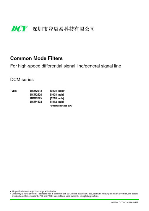
DCM4532[1812 inch]DCM3225[1210 inch]DCM2520[1008 inch]DCM2012[0805 inch]*DCM series•All specifications are subject to change without notice.•Conformity to RoHS Directive: This means that, in conformity with EU Directive 2002/95/EC, lead, cadmium, mercury, hexavalent chromium, and specific bromine-based flame retardants, PBB and PBDE, have not been used, except for exempted applications.Common Mode FiltersFor high-speed differential signal line/general signal line Type:* Dimensions Code [EIA](6) internal codeDCM4532DCM3225DCM2520DCM2012DCM Series DCM2012, 2520, 3225, 4532DCM 2012 -900-2P -T Common Mode FiltersFor High-speed Differential Signal Line / General Signal LineFEATURES•Although greatly miniaturized, this wire-wound chip-type filter maintains the characteristics needed for a common mode filter. Common mode impedance is 1000Ω [at 100MHz], so this filter is greatly effective in supporting noise.•Almost no affect upon even high speed signals since differential mode impedance is kept low.•This series includes both 2-line and 3-line types. They are used for various types of circuits and noise.APPLICATIONS•Used for radiation noise suppression for any electronic devices. •Used to counter common mode noise affecting signals within high-speed lines.•USB line for personal computers and peripheral equipment. •IEEE1394 line for personal computers, DVC, STB, etc.•LVDS, panel link line for liquid crystal display panels.TEMPERATURE RANGESPACKAGING STYLE AND QUANTITIESPRODUCT IDENTIFICATION (1) Series name(2) Dimensions L ×W 2012: 2.0×1.2mm(3) Impedance[at 100MHz]900: 90Ω(4) Number of line2P: 2-line 3P: 3-line(5) Packaging styleT: ø180mm reel taping TL: ø330mm reel taping RECOMMENDED SOLDERING CONDITIONS RECOMMENDED TEMPERATURE PROFILE FOR LEAD-FREE SOLDERREFLOW PROFILE FOR SOLDER HEAT RESISTANCEConformity to RoHS Directive Operating–25 to +85°C Storage(After mount)–25 to +85°CPackaging styleT ype Reel QuantityT apingø180mm 2000 pieces/reel ø330mm 10000 pieces/reel ø180mm 2000 pieces/reel ø330mm 10000 pieces/reel ø180mm 1000 pieces/reel ø330mm 5000 pieces/reel ø180mm 500 pieces/reel ø330mm2000 pieces/reel(1)(2)(3)(4)(5)(6)DCM2520-3P DCM4532-102-3PDCM2520-2P DCM3225-2PDCM2012-2PSHAPES AND DIMENSIONS/CIRCUIT DIAGRAMS/RECOMMENDED PC BOARD PATTERNS 2-LINE TYPE 3-LINE TYPEDCM4532-102-3P10000.6200.2DCM2520-801-3P 800 1.6200.15DCM3225-102-2P 10000.5200.2DCM3225-271-2P 2700.3200.3DCM3225-161-2P 1600.2200.35DCM3225-800-2P 800.15200.4DCM2520-102-2P 10000.9200.2DCM2520-601-2P 6000.45200.3DCM2520-451-2P 4500.4200.35DCM2520-301-2P 3000.35200.4DCM2012-361-2P 3600.5500.22DCM2012-201-2P 2000.25500.35DCM2012-121-2P 1200.22500.37DCM2012-900-2P 900.19500.4ELECTRICAL CHARACTERISTICSPart No.Impedance(Ω)typ.[100MHz]DC resistance(Ω)max.[per 1 line]Rated voltage Edc(V)max.Rated current Idc(A)max.2-LINE3-LINEDCM3225-271-2P DCM3225-102-2PDCM3225-800-2P DCM3225-161-2PDCM2520-601-2P DCM2520-102-2PDCM2520-301-2P DCM2520-451-2PDCM2012-201-2P DCM2012-361-2PDCM2012-900-2P DCM2012-121-2PMEASURING CIRCUITS 2-LINEDCM2520-801-3P DCM4532-102-3PIMPEDANCE vs. FREQUENCY CHARACTERISTICS 3-LINEMEASURING CIRCUITS 3-LINE。
共模电感资料

Q/DNXXXX-2005前言本规范是总规范GJB 1435-92《开关电源变压器总规范》的相关详细规范。
本规范的附录A是资料性附录。
本规范由北京德恩电子有限公司起草本规范主要起草人:本规范审核人:质量:工艺:本规范标准化人:本规范批准人:Q/DNXXXX-2005XXXXX型共模电感器详细规范1 范围1.1 主题内容本规范规定了XXXXX型共模电感器(以下简称“共模电感器”)的详细要求、质量保证规定和试验方法。
1.2 适用范围本规范适用于XXXXX型共模电感器的生产和试验。
1.3 分类1.3.1 型号规格本规范规定的共模电感器型号规格为XXXXX型。
1.3.2类别由于本规范所参照及引用的GJB 1435-92是开关电源变压器的总规范,按照总规范应规定变压器的类别,XXXXX型是共模电感器,因此未在本规范中规定类别,凡是涉及到与类别有关的试验,均按GJB 1435-92 中有关8类的规定执行。
2 引用文件下列文件的有关条款通过引用而构成为本规范的条款。
凡注日期或版次的引用文件,其后的任何修改单(不包括勘误的内容)或修订版本都不适用于本规范,但提倡使用本规范的各方面探讨使用其最新版本的可能性,凡不注日期或版次的引用文件,其最新版本适用于本规范。
GJB 360A—96 电子及电气元件试验方法GJB 1435—92 开关电源变压器总规范GJB 4027-2000 军用电子元器件破坏性物理分析方法3 要求3.1 总则共模电感器应符合本规范和GJB 1435-92总规范的规定。
本规范的要求与总规范不一致时,应以本规范为准。
3.2 材料制造共模电感器的磁芯应符合“XXXX”的有关规定,其它材料要求见附录A(补充件)。
3.3 设计和结构3.3.1 外形尺寸结构共模电感器的外形构见图1,引出线端的引出方向及结构应与图1相一致,外形尺寸应符合表1规定,单位为毫米。
图1电原理图见图2,线径和匝数见表234图23.3.3 重量最大重量: XXg ; 3.4 工作温度范围-55℃~+105℃ 3.5工作电压、电流、频率V , A , kHz 。
共模电感规格书

共模电感规格书一、引言共模电感是一种用于抑制电磁干扰的重要电子元件。
它广泛应用于各种电子设备中,起到滤波、隔离和抑制共模干扰的作用。
本规格书将详细介绍共模电感的技术参数和性能指标,以便用户正确选择和应用共模电感。
二、产品概述共模电感是一种具有双绕组结构的电感器件。
它通常由磁性材料制成,具有较高的感应电感和较低的串扰电感。
根据不同的应用场景和需求,共模电感可分为各种规格和尺寸,具备不同的电气参数和性能特点。
三、技术参数1. 电感值:共模电感的电感值是衡量其性能的重要参数之一。
它通常用于表示电感器件对电流变化的响应能力,单位为亨利(H)。
根据不同的应用需求,共模电感的电感值范围从几微亨到数亨不等。
2. 额定电流:共模电感的额定电流是指在额定工作条件下,电感器件能够正常工作的最大电流值。
它通常由电感器件的内部结构、材料和散热设计等因素决定。
额定电流的选择应根据实际应用中的电流要求和安全裕度进行确定。
3. 阻抗范围:共模电感的阻抗范围是指在工作频率范围内,电感器件对电流的阻碍程度。
它通常由电感器件的电感值和串扰电感值共同决定。
合理选择阻抗范围能够有效抑制共模干扰,提高系统的抗干扰能力。
4. 频率特性:共模电感的频率特性是指其电感值在不同频率下的变化情况。
电感值随频率的变化可以是线性的、非线性的或者具有谐振点等特性。
了解共模电感的频率特性有助于在实际应用中准确选择和设计共模滤波电路。
5. 尺寸和结构:共模电感的尺寸和结构决定了它在电子设备中的安装方式和空间占用。
常见的共模电感结构有线圈式、环形式、片式等,尺寸从微米级到毫米级不等。
根据实际应用的场景和要求,选择合适的尺寸和结构能够有效提高共模电感的性能和可靠性。
四、性能指标1. 温度特性:共模电感的温度特性是指其电感值随温度变化的情况。
温度变化会引起电感器件内部材料的热膨胀和电学性能的变化,从而影响电感值的稳定性。
合理选择具有良好温度特性的共模电感,能够确保系统在不同温度环境下的稳定性和可靠性。
共模电感原厂规格书
DCM4532[1812 inch]DCM3225[1210 inch]DCM2520[1008 inch]DCM2012[0805 inch]*DCM series•All specifications are subject to change without notice.•Conformity to RoHS Directive: This means that, in conformity with EU Directive 2002/95/EC, lead, cadmium, mercury, hexavalent chromium, and specific bromine-based flame retardants, PBB and PBDE, have not been used, except for exempted applications.Common Mode FiltersFor high-speed differential signal line/general signal line Type:* Dimensions Code [EIA](6) internal codeDCM4532DCM3225DCM2520DCM2012DCM Series DCM2012, 2520, 3225, 4532DCM 2012 -900-2P -T Common Mode FiltersFor High-speed Differential Signal Line / General Signal LineFEATURES•Although greatly miniaturized, this wire-wound chip-type filter maintains the characteristics needed for a common mode filter. Common mode impedance is 1000Ω [at 100MHz], so this filter is greatly effective in supporting noise.•Almost no affect upon even high speed signals since differential mode impedance is kept low.•This series includes both 2-line and 3-line types. They are used for various types of circuits and noise.APPLICATIONS•Used for radiation noise suppression for any electronic devices. •Used to counter common mode noise affecting signals within high-speed lines.•USB line for personal computers and peripheral equipment. •IEEE1394 line for personal computers, DVC, STB, etc.•LVDS, panel link line for liquid crystal display panels.TEMPERATURE RANGESPACKAGING STYLE AND QUANTITIESPRODUCT IDENTIFICATION (1) Series name(2) Dimensions L ×W 2012: 2.0×1.2mm(3) Impedance[at 100MHz]900: 90Ω(4) Number of line2P: 2-line 3P: 3-line(5) Packaging styleT: ø180mm reel taping TL: ø330mm reel taping RECOMMENDED SOLDERING CONDITIONS RECOMMENDED TEMPERATURE PROFILE FOR LEAD-FREE SOLDERREFLOW PROFILE FOR SOLDER HEAT RESISTANCEConformity to RoHS Directive Operating–25 to +85°C Storage(After mount)–25 to +85°CPackaging styleT ype Reel QuantityT apingø180mm 2000 pieces/reel ø330mm 10000 pieces/reel ø180mm 2000 pieces/reel ø330mm 10000 pieces/reel ø180mm 1000 pieces/reel ø330mm 5000 pieces/reel ø180mm 500 pieces/reel ø330mm2000 pieces/reel(1)(2)(3)(4)(5)(6)DCM2520-3P DCM4532-102-3PDCM2520-2P DCM3225-2PDCM2012-2PSHAPES AND DIMENSIONS/CIRCUIT DIAGRAMS/RECOMMENDED PC BOARD PATTERNS 2-LINE TYPE 3-LINE TYPEDCM4532-102-3P10000.6200.2DCM2520-801-3P 800 1.6200.15DCM3225-102-2P 10000.5200.2DCM3225-271-2P 2700.3200.3DCM3225-161-2P 1600.2200.35DCM3225-800-2P 800.15200.4DCM2520-102-2P 10000.9200.2DCM2520-601-2P 6000.45200.3DCM2520-451-2P 4500.4200.35DCM2520-301-2P 3000.35200.4DCM2012-361-2P 3600.5500.22DCM2012-201-2P 2000.25500.35DCM2012-121-2P 1200.22500.37DCM2012-900-2P 900.19500.4ELECTRICAL CHARACTERISTICSPart No.Impedance(Ω)typ.[100MHz]DC resistance(Ω)max.[per 1 line]Rated voltage Edc(V)max.Rated current Idc(A)max.2-LINE3-LINEDCM3225-271-2P DCM3225-102-2PDCM3225-800-2P DCM3225-161-2PDCM2520-601-2P DCM2520-102-2PDCM2520-301-2P DCM2520-451-2PDCM2012-201-2P DCM2012-361-2PDCM2012-900-2P DCM2012-121-2PMEASURING CIRCUITS 2-LINEDCM2520-801-3P DCM4532-102-3PIMPEDANCE vs. FREQUENCY CHARACTERISTICS 3-LINEMEASURING CIRCUITS 3-LINE。
giantechyaozan common mode choke series巨泰天祥公司共模电感线圈规格系列

Solder Heat Resistance
Component Adhesion (Push test)
Component Adhesion (Pull test)
2012F2S-900T04 2.0±0.2 1.2±0.2 1.2±0.2 0.55±0.1 0.46±0.1 0.15±0.1
2012F2S-SERIES 2.0±0.2 1.2±0.2 1.2±0.2 0.4±0.1 0.4±0.1 0.15±0.1
3.PUnaitsr:tmNmumbering
100
0.30
400
50
125
10M
WCM2012F2S-161T03 160±25%
100
0.35
350
50
125
10M
WCM2012F2S-181T03 180±25%
100
0.35
350
50
125
10M
WCM2012F2S-221T03 220±25%
100
0.40
300
50
125
10M
WCM2012F2S-261T03 260±25%
Test Condition
Temperature:85 5 Time:500 12hr.
Recovery: 4 to 24hrs of recovery under the standard condition after the removal from test chamber.
绕组铁氧体 NLV32-PFD 3225 产品说明书
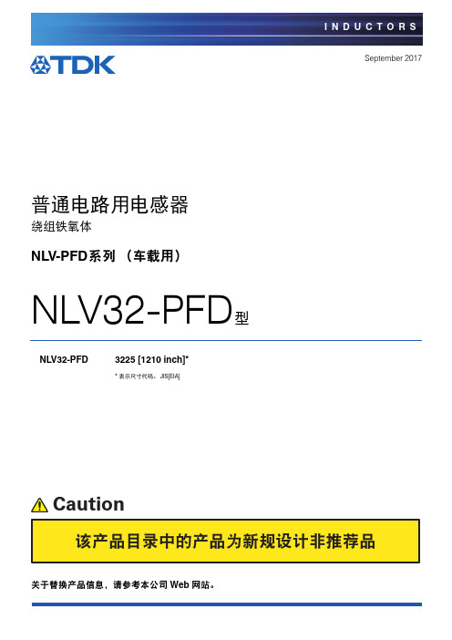
I N D U C T O R SSeptember 2017普通电路用电感器绕组铁氧体NLV-PFD系列(车载用)NLV32-PFD型NLV32-PFD3225 [1210 inch]** 表示尺寸代码。
JIS[EIA]Caution使用注意事项在使用本产品前,请务必随附采购规格书。
安全注意事项使用本产品时,请注意安全事项。
保存时间为6个月以内,保存条件(温度5~40°C 、湿度10~75%RH 以下),需充分注意。
若超过保存时间,端子电极的可焊性将可能老化。
请勿在气体腐蚀环境(盐、酸、碱等)下使用和保管。
在实施焊接前,请务必进行预热。
预热温度与焊接温度及芯片温度的温度差要在150°C 以内。
安装后的焊接修正应在规格书规定的条件范围内。
若加热过度可能导致短路、性能降低、寿命减少。
将安装了芯片的印刷电路组装到装置时,请注意不要因印刷电路整体变形或紧固部等局部变形而给芯片施加剩余应力。
装置会因通电而自我发热(温度上升),因此在热设计方面需留有充分余地。
非磁屏蔽型在基板设计时需注意配置线圈。
受到电磁干扰可能会导致误动作。
由于人体所带的静电会传到接地线上,因此请使用防静电腕带。
请勿将本产品靠近磁铁或带有磁力的物体。
请在采购规格书规定的范围内使用。
本产品目录中记载的产品是指在通用标准用途意义上使用于一般电子设备(AV 设备,通信设备,家电产品,娱乐设备,计算机设备,个人设备,办公设备,计测设备,工业机器人),并且该一般电子设备要在通常的操作和使用方法下使用。
对于需要高度安全性和可靠性的,或者设备的故障,误动作,运转不良可能会给人的生命,身体及财产等造成损害,以及有可能产生莫大社会影响的以下用途(以下称‘特定用途’)中的适用性,性能发挥,品质,本公司不予保证。
客户预定在本产品目录的范围,条件之外,或者在特定用途中使用时,请事先咨询本公司相关部门。
本公司会配合客户需求,一起协商不同于本产品目录中所记载的使用用途。
- 1、下载文档前请自行甄别文档内容的完整性,平台不提供额外的编辑、内容补充、找答案等附加服务。
- 2、"仅部分预览"的文档,不可在线预览部分如存在完整性等问题,可反馈申请退款(可完整预览的文档不适用该条件!)。
- 3、如文档侵犯您的权益,请联系客服反馈,我们会尽快为您处理(人工客服工作时间:9:00-18:30)。
DCM4532
[1812 inch]
DCM3225[1210 inch]DCM2520[1008 inch]DCM2012[0805 inch]*DCM series
•All specifications are subject to change without notice.
•Conformity to RoHS Directive: This means that, in conformity with EU Directive 2002/95/EC, lead, cadmium, mercury, hexavalent chromium, and specific bromine-based flame retardants, PBB and PBDE, have not been used, except for exempted applications.
Common Mode Filters
For high-speed differential signal line/general signal line Type:
* Dimensions Code [EIA]
(6) internal code
DCM4532
DCM3225DCM2520
DCM2012DCM Series DCM2012, 2520, 3225, 4532
DCM 2012 -900-2P -T Common Mode Filters
For High-speed Differential Signal Line / General Signal Line
FEATURES
•Although greatly miniaturized, this wire-wound chip-type filter maintains the characteristics needed for a common mode filter. Common mode impedance is 1000Ω [at 100MHz], so this filter is greatly effective in supporting noise.
•Almost no affect upon even high speed signals since differential mode impedance is kept low.
•This series includes both 2-line and 3-line types. They are used for various types of circuits and noise.
APPLICATIONS
•Used for radiation noise suppression for any electronic devices. •Used to counter common mode noise affecting signals within high-speed lines.
•USB line for personal computers and peripheral equipment. •IEEE1394 line for personal computers, DVC, STB, etc.•LVDS, panel link line for liquid crystal display panels.TEMPERATURE RANGES
PACKAGING STYLE AND QUANTITIES
PRODUCT IDENTIFICATION (1) Series name
(2) Dimensions L ×W 2012: 2.0×1.2mm
(3) Impedance[at 100MHz]
900: 90Ω
(4) Number of line
2P: 2-line 3P: 3-line
(5) Packaging style
T: ø180mm reel taping TL: ø330mm reel taping RECOMMENDED SOLDERING CONDITIONS RECOMMENDED TEMPERATURE PROFILE FOR LEAD-FREE SOLDER
REFLOW PROFILE FOR SOLDER HEAT RESISTANCE
Conformity to RoHS Directive Operating
–25 to +85°C Storage(After mount)
–25 to +85°C
Packaging style
T ype Reel Quantity
T aping
ø180mm 2000 pieces/reel ø330mm 10000 pieces/reel ø180mm 2000 pieces/reel ø330mm 10000 pieces/reel ø180mm 1000 pieces/reel ø330mm 5000 pieces/reel ø180mm 500 pieces/reel ø330mm
2000 pieces/reel
(1)
(2)(3)(4)(5)
(6)
DCM2520-3P DCM4532-102-3P
DCM2520-2P DCM3225-2P
DCM2012-2P
SHAPES AND DIMENSIONS/CIRCUIT DIAGRAMS/RECOMMENDED PC BOARD PATTERNS 2-LINE TYPE 3-LINE TYPE
DCM4532-102-3P
1000
0.6
20
0.2
DCM2520-801-3P 800 1.6200.15DCM3225-102-2P 10000.5200.2DCM3225-271-2P 2700.3200.3DCM3225-161-2P 1600.2200.35DCM3225-800-2P 800.15200.4DCM2520-102-2P 10000.9200.2DCM2520-601-2P 6000.45200.3DCM2520-451-2P 4500.4200.35DCM2520-301-2P 3000.35200.4DCM2012-361-2P 3600.5500.22DCM2012-201-2P 2000.25500.35DCM2012-121-2P 1200.22500.37DCM2012-900-2P 900.19500.4ELECTRICAL CHARACTERISTICS
Part No.
Impedance
(Ω)typ.[100MHz]DC resistance
(Ω)max.[per 1 line]Rated voltage Edc(V)max.Rated current Idc(A)max.2-LINE
3-LINE
DCM3225-271-2P DCM3225-102-2P
DCM3225-800-2P DCM3225-161-2P
DCM2520-601-2P DCM2520-102-2P
DCM2520-301-2P DCM2520-451-2P
DCM2012-201-2P DCM2012-361-2P
DCM2012-900-2P DCM2012-121-2P
MEASURING CIRCUITS 2-LINE
DCM2520-801-3P DCM4532-102-3P
IMPEDANCE vs. FREQUENCY CHARACTERISTICS 3-LINE
MEASURING CIRCUITS 3-LINE。