芯片封装 焊线动画_wirebonding
芯片Wire bonding引线键合导线键合绑定教程-70页
Wire bonding 引线键合/导线键合/绑定什么是导线键合用金属丝将芯片的I/O端与对应的封装引脚或者基板上布线焊区互连,固相焊接过程,采用加热、加压和超声能,破坏表面氧化层和污染,产生塑性变形,界面亲密接触产生电子共享和原子扩散形成焊点,键合区的焊盘金属一般为Al或者Au等,金属细丝是直径为几十到几百微米的Au、Al或者Si-Al丝。
应用范围低成本、高可靠、高产量等特点使得它成为芯片互连的主要工艺方法,用于下列封装::•陶瓷和塑料BGA、单芯片或者多芯片•陶瓷和塑料(CerQuads and PQFPs)•芯片尺寸封装(CSPs)•板上芯片(COB)Virtually all dynamic random access memory (DRAM) chips and most commodity chips in plastic packages are assembled by wirebonding. About 1.2-1.4 trillion wire interconnections are produced annually. Manufacturing losses and test failures are about 40-1000 ppm and trending downward each year.历史和特点1957 年Bell实验室采用的器件封装技术,目前特点如下:¾已有适合批量生产的自动化机器,¾键合参数可精密控制,导线机械性能重复性高,¾速度可达100-125ms/互连(两个焊接和一个导线循环过程),¾间距达50 um 而高度可低于,¾劈刀的改进解决了大多数的可靠性问题¾根据特定的要求,出现了各种工具和材料可供选择,¾已经形成非常成熟的体系。
芯片互连例子采用导线键合的芯片互连三种键合(焊接)机理超声焊接:利用超声波(60~120KHz)发生器使劈刀发生水平弹性振动,同时施加向下的压力。
COB wire_bonding原理介绍
• Tool less conversion window clamps and top plate enables fast device
Eagle
MACHINE SPECIFICATIONS (I) •Bonding System •Bonding Method Thermosonic (TS) •BQM Mode Constant Current, Voltage, Power and Normal (Programmable) •Loop Type Normal, Low, Square & J •XY Resolution 0.2 um •Z Resolution (capillary travelling motion)2.5 um •Fine Pitch Capability 35 mm pitch @ 0.6 mil wire •No. of Bonding Wires up to 1000 •Program Storage 1000 programs on Hard Disk •Multimode Transducer System Programmable profile, control and vibration modes
SEARCH SPEED1
pad
SEARCH TOL 1
lead
Free air ball is captured in the chamfer
SEARCH SPEED1
pad
SEARCH TOL 1
lead
Free air ball is captured in the chamfer
SEARCH SPEED1
PRESSURE
Ultra
Sonic
Vibration
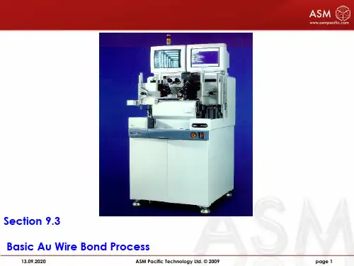
ASM 自动焊线机器介绍Au wire bonding process ppt课件
page 11
Comparison of Different Wire Bonding Techniques
Wirebonding
Thermocompression
Operating Temperature
300-500°C
Wire Materials
Au
Pad Materials
Al, Au
Note
Thermosonic bonding: utilizes temperature, ultrasonic and low impact force, and ball/ wedge methods.
Ultrasonic bonding: utilizes ultrasonic and low impact force, and the weer Grinding
Wafer Saw
Die Bonding
Toaster
Wire Bonding
Die Surface Coating
Molding
Laser Mark
BGA
SURFACE MOUNTPKG THROUGH HOLE PKG
13.09.2020
Solder Ball Placement
Wedge Bond ( 2nd Bond )
Gold wire
Die Pad
Lead
13.09.2020
ASM Pacific Technology Ltd. © 2009
page 6
Wedge Bonding
13.09.2020
ASM Pacific Technology Ltd. © 2009
Dejunk Trim
Solder Plating
Wire-Bonding工艺以及基本知识 PPT
Capillary的選用:
Hole径(H)
Hole径是由规定的Wire径WD(Wire Diameter)
来決定
H
H=1.2~1.5WD
WD
Capillary主要的尺寸:
H:Hole Diameter (Hole径) T:Tip Diameter B:Chamfer Diameter(orCD) IC:Inside Chamfer IC ANGLE:Inside Chamfer Angle FA:Face Angle (Face角) OR:Outside Radius
Die 第一焊点搜索速度1st Search Speed 1
3. 第一焊點接触階段
最初的球形影响参数: 接觸压力和预备功率 Impact Force and Standby Power
1/16 inch 總長L
Capillary尺寸對焊線品質的影響:
1. Chamfer径(CD) Chamfer径过于大的话、Bonding強度越弱,易造成虛焊.
CD
CD
大家应该也有点累了,稍作休息
大家有疑问的,可以询问和交流
2. Chamfer角(ICA ) Chamfer角:小→Ball Size:小 Chamfer角:大→Ball Size:大
1.Wire Bonding原理
IC封裝中電路連接的三種方式: a. 倒裝焊(Flip chip bonding) b. 載帶自動焊(TAB---tape automated bonding) c. 引線鍵合(wire bonding)
Wire Bonding------引線鍵合技術
Wire Bonding的作用
Wire Bonding的四要素: ➢ Time(時間) ➢ Power(功率) ➢ Force(壓力) ➢ Temperature(溫度)
引线键合(WireBonding)
引线键合(WireBonding)引线键合(Wire Bonding)——将芯片装配到PCB上的方法 | SK hynix Newsroom结束前工序的每一个晶圆上,都连接着500~1200个芯片(也可称作Die)。
为了将这些芯片用于所需之处,需要将晶圆切割(Dicing)成单独的芯片后,再与外部进行连接、通电。
此时,连接电线(电信号的传输路径)的方法被称为引线键合(Wire Bonding)。
其实,使用金属引线连接电路的方法已是非常传统的方法了,现在已经越来越少用了。
近来,加装芯片键合(Flip Chip Bonding)和硅穿孔(Through Silicon Via,简称TSV)正在成为新的主流。
加装芯片键合也被称作凸点键合(Bump Bonding),是利用锡球(Solder Ball)小凸点进行键合的方法。
硅穿孔则是一种更先进的方法。
为了了解键合的最基本概念,在本文中,我们将着重探讨引线键合,这一传统的方法。
一、键合法的发展历程图1. 键合法的发展史:引线键合(Wire Bonding)→加装芯片键合(Flip Chip Bonding)→硅穿孔(TSV)下载图片为使半导体芯片在各个领域正常运作,必须从外部提供偏压(Bias voltage)和输入。
因此,需要将金属引线和芯片焊盘连接起来。
早期,人们通过焊接的方法把金属引线连接到芯片焊盘上。
从1965年至今,这种连接方法从引线键合(Wire Bonding),到加装芯片键合(Flip Chip Bonding),再到TSV,经历了多种不同的发展方式。
引线键合顾名思义,是利用金属引线进行连接的方法;加装芯片键合则是利用凸点(bump)代替了金属引线,从而增加了引线连接的柔韧性;TSV作为一种全新的方法,通过数百个孔使上下芯片与印刷电路板(Printed Circuit Board,简称PCB)相连。
二、键合法的比较:引线键合(Wire Bonding)和加装芯片键合(Flip Chip Bonding)图2. 引线键合(Wire Bonding) VS加装芯片键合(Flip Chip Bonding)的工艺下载图片三、引线键合(Wire Bonding)是什么?图3. 引线键合的结构(载体为印刷电路板(PCB)时)下载图片引线键合是把金属引线连接到焊盘上的一种方法,即是把内外部的芯片连接起来的一种技术。
Wire_Bond焊线动作分解说明
pad
lead
Capillary rises to loop height position
RH
pad
lead
Formation of a loop
RD (Reverse Distance)
pad
lead
Formation of a loop
pad
lead
pad
lead
WIRE CLAMP ‘CLOSE’
Wafer Grinding
封裝流程
Wafer Saw
Die Bonding
toaster
Wire Bonding
Die Surface Coating
Molding
Laser Mark
BGA
SURFACE MOUNTPKG THROUGH HOLE PKG
Solder Ball Placement
Dejunk TRIM Solder Plating
Singulation
Solder Plating TRIM/ FORMING
FORMING/ Singulation
Packing
Wire Bond 原理
Ball Bond ( 1st Bond )
Wedge Bond ( 2nd Bond )
SEARCH SPEED1
pad
SEARCH TOL 1
lead
Free air ball is captured in the chamfer
SEARCH SPEED1
pad
SEARCH TOL 1
lead
Free air ball is captured in the chamfer
Wire-Bonding工艺介绍和Gold-Wire特性
金线焊接工具---劈刀
劈刀决定的一些参数: 1、Bond Pad Pitch
金线焊接工具---劈刀
T--Tip Diameter, BTNK—Bottleneck Height&Angle, CA—Cone Angle Will affect bond pad pitch.
2、1st Bond Diameter
Not move
affect Not affect
Go up with capillary
Form ball when 6000v on it
Not affect Not affect
金线球形焊接工艺介绍
Stage1
Stage2
Stage3
Stage4
Stage5
Stage6
Stage7
Stage8
H—Hole Diameter, ICA—Inner Chamfer Angle CD—Chamfer Diameter Will affect 1st bond diameter
金线焊接工具---劈刀
3、Wire Diameter
H—Hole Diameter
Hole diameter is usually 1.5X wire diameter
wire
Ultrasonic and force
Form ball when 6000v on it
Not affect
Go up to chamfer, affect touch die surface
Not move
Not affect
Form loop shape Not affect
Squashed and form 2nd bond
半导体wire bond工艺流程
半导体wire bond工艺流程下载温馨提示:该文档是我店铺精心编制而成,希望大家下载以后,能够帮助大家解决实际的问题。
文档下载后可定制随意修改,请根据实际需要进行相应的调整和使用,谢谢!并且,本店铺为大家提供各种各样类型的实用资料,如教育随笔、日记赏析、句子摘抄、古诗大全、经典美文、话题作文、工作总结、词语解析、文案摘录、其他资料等等,如想了解不同资料格式和写法,敬请关注!Download tips: This document is carefully compiled by theeditor. I hope that after you download them,they can help yousolve practical problems. The document can be customized andmodified after downloading,please adjust and use it according toactual needs, thank you!In addition, our shop provides you with various types ofpractical materials,such as educational essays, diaryappreciation,sentence excerpts,ancient poems,classic articles,topic composition,work summary,word parsing,copy excerpts,other materials and so on,want to know different data formats andwriting methods,please pay attention!半导体 Wire Bond 工艺流程。
1. 焊盘镀层。
WireBonding工艺以和基本知识PPT培训课件
Ball Offset
Capillary Center line
Ball Center line
die 的方 向
lead 的方向
Capillary center -60
Capillary center 60
计算线长 Calculate d Wire Length
DI E
线夹关上 - WIRE CLAMP CLOSE
焊头向上运动 BOND HEAD MOVE UP
CONFIDENTIAL
8. 搜索延遲
搜索延迟 - XY 工作台向第二压点移动 - 焊头不动 SEARCH DELAY - XY TABLE MOVE TOWARDS 2ND BOND - BH MOTIONLESS
动作 焊头下降至第一焊点 之搜索高度 第一焊点之搜索 第一焊点的接触阶段 第一焊点的焊接阶段 返回高度 返回距离 估计线长高度 搜索延迟 焊头下降至第二焊点 之搜索高度 第二焊点之搜索 第二焊点的接触阶段 第二焊点的焊接阶段 线尾长度 焊头回到原始位置
CONFIDENTIAL
焊头動作步驟 1. 焊头在打火高度( 复位位置 )
焊头向上运动 BOND HEAD MOVE UP
反向高度 - RH DIE
CONFIDENTIAL
6. 反向距离
线夹打开 WIRE CLAMP“Open”
反向距离-RD
DIEIE
XY 工作台运动 X-Y TABLE MOVEMENT
CONFIDENTIAL
7. 焊头上升到线弧高度位置
线夹关上后, 开始第一点压 焊检测 M/C START TO DO THE 1ST BOND NON STICK DETECTION AT LOOP TOP POSITION AFTER W/C CLOSE
COB工艺制程简介
COB工艺制程简介1.芯片的焊线连接:1.1芯片直接封装简介:现代消费性电子产品逐渐走向轻、薄、短、小的潮流下,COB(Chip On Board)已成为一种普遍的封装技术。
COB的关键技术在于Wire Bonding(俗称打线)及Molding (封胶成型),是指对裸露的集成电路芯片(IC Chip),进行封装,形成电子组件的制程,其中IC藉由焊线(Wire Bonding)、覆晶接合(Flip Chip)、或卷带接合(Tape Automatic Bonding;简称TAB)等技术,将其I/O经封装体的线路延伸出来。
集成电路芯片必须依照设计和外界的电路连接,方能成为具有一定功能的电子组件就如我们所看到的"IC"就是这种已封装好、有外引脚的封装的集成电路。
1.2芯片的焊线连接方式简介:IC芯片必须与封装基板完成电路连接才能发挥既有的功能,现时市面上流行的焊线连接方式有三类 :打线接合(Wire Bonding)、卷带自动接合(Tape Automated Bonding,TAB)与覆晶接合(Flip Chip,FC),分述如下:1.2.1打线接合(Wire Bonding)打线接合是最早亦为目前应用最广的技术,此技术首先将芯片固定于导线架上,再以细金属线将芯片上的电路和导线架上的引脚相连接。
而随着近年来其它技术的兴起,打线接合技术正受到挑战,其市场占有比例亦正逐渐减少当中。
但由于打线接合技术之简易性及便捷性,加上长久以来与之相配合之机具、设备及相关技术皆以十分成熟,因此短期内打线接合技术似乎仍不大容易为其它技术所淘汰。
图1.2a打线接合的示意图1.2.2卷带式自动接合(Tape Automated Bonding,TAB)卷带式自动接合技术首先于1960年代由通用电子(GE)提出。
卷带式自动接合制程,即是将芯片与在高分子卷带上的金属电路相连接。
而高分子卷带之材料则以polyamide为主,卷带上之金属层则以铜箔使用最多。
- 1、下载文档前请自行甄别文档内容的完整性,平台不提供额外的编辑、内容补充、找答案等附加服务。
- 2、"仅部分预览"的文档,不可在线预览部分如存在完整性等问题,可反馈申请退款(可完整预览的文档不适用该条件!)。
- 3、如文档侵犯您的权益,请联系客服反馈,我们会尽快为您处理(人工客服工作时间:9:00-18:30)。
lead
pad
leadpadle来自dpadlead
pad
lead
Formation of a second bond
pad
heat
lead
Formation of a second bond
pad
heat
lead
pad
heat
lead
pad
heat
lead
pad
lead
pad
lead
pad
lead
Formation of a first bond
PRESSURE
Ultra Sonic Vibration
pad
heat
lead
Formation of a first bond
PRESSURE
Ultra Sonic Vibration
pad
heat
lead
Capillary rises to loop height position
Semiconductor Packaging Process
WAFER
WAFER MOUNT
WAFER SAW
DIE ATTACH
MODING
WIRE BOND
EPOXY CURE
TRIM / FORM
Integrated Circuit (IC)
CONTENTS
• A. PURPOSE • B. PRINCIPLE • C. PROCESS • D. PACKAGE INTODUCE • E. M/C BASIC DATA • F. MATERIAL • G. PARAMETER • H. DEFECTS • I. REFERENCE
A.PURPOSE
• FORMING A STRONG AND RELIABLE INTERTALLIC BOND BETWWEEN THE WIRE AND THE PAD , AS WELL AS BETWEEN THE WIRE AND THE LEAD
DICE GOLD WIRE LEADFRAME
Si
MOISTURE
C. WIREBOND PROCESS
Free air ball is captured in the chamfer
GOLD BALL
pad lead
Free air ball is captured in the chamfer
pad lead
Free air ball is captured in the chamfer
A.PURPOSE
Ball Bond ( 1st Bond )
Wedge Bond ( 2nd Bond )
Gold wire
pad lead
B.PRINCIPLE
• HARD WELDING:
– PRESSURE – AMPLIFY & FREQUENCY – WELDING TIME – WELDING TEMPATURE
pad
lead
pad
lead
pad
lead
pad
lead
Disconnection of the tail
pad
lead
Disconnection of the tail
pad
lead
Formation of a new free air ball
pad
lead
pad
lead
Formation of a loop
pad
lead
Formation of a loop
pad
lead
pad
lead
pad
lead
pad
lead
pad
lead
pad
lead
pad
lead
pad
lead
pad
lead
pad
lead
pad
lead
pad
lead
pad
pad
lead
Capillary rises to loop height position
pad
lead
Capillary rises to loop height position
pad
lead
Capillary rises to loop height position
pad
lead
Capillary rises to loop height position
pad
lead
Free air ball is captured in the chamfer
pad
lead
Free air ball is captured in the chamfer
pad
lead
Formation of a first bond
pad
lead
Formation of a first bond
• THERMOSONIC BONDING:
– THERMAL COMPRESSURE – ULTRASONIC ENERGY(1.2MHZ)
B.PRINCIPLE
PRESSURE VIBRATION
AL2O3
CONTAMINATION GLASS
GOLD BALL
Al SiO2, TiN, TiW