国巨电容规格书CC系列
YAGEO电容规格书

Y5V ∆C/C ≤ 20% -10% ≤ ∆C/C ≤ 20%
∆C/C: ≤ 20%
-40% ≤ ∆C/C ≤ 30% Tanδ: ≤ 7%, 12.5%, 15% IR: 1000MΩ or RxC ≥ 25s Whichever is less
-40% ≤ ∆C/C ≤ 30% Tan δ: ≤ 7%, 12.5%, 15% IR: 2000MΩ or RxC ≥ 50s Whichever is less
-3-
YAGEO CORPORATION
Aging Rate
Aging Curve ∆C/C (%) 10
0
-10
NPO X7R Y5V
-20
-30 1 10 100 1000 Hours
-4-
YAGEO CORPORATION
Reflow Profile
Temp
℃
245 225 235±10
183 150
Rins > 10GΩ or RinsxC≥500s, whichever is less. No breakdown
Rins > 10GΩ or RinsxC≥500s, Whichever is less.
Rins > 10GΩ or RinsxC≥100s, whichever is less.
Code 7 Capacitance tolerance A = ±0.05pF G = ±2% B = ±0.1pF J = ±5% C = ±0.25pF K = ±10% D = ±0.5pF M = ±20% F = ±1% Z= -20%+80% Code 8 Packing style R = Paper tape reel ϕ 7 inch P = Paper tape reel ϕ 13 inch K = Embossed plastic tape reel ϕ 7 inch. F = Embossed plastic tape reel ϕ 13 inch. B = Bulk Bag C = Bulk Cassette Code 9~11 Material
插件国巨电阻规格书
Page-1Approval SheetforCarbon Film ResistorsCFR series±2% & ±5%YAGEO CORPORATIONHeadquarters: 3F, No.233-1, Pao Chiao Rd., Shin Tien, Taipei, Taiwan,R.O.C.Tel: 886-2-2917-7555 Fax: 886-2-2917-4286URL: Page-2Page-31. PRODUCT : CARBON FILM RESISTORS(Normal & Miniature Style)2. PART NUMBER : Part number of the carbon film resistor is identified by the name,power, tolerance, packing, temperature coefficient, special type and resistance value.Example :CFR -12 J T J 52 100RSeries Size Resistance Packing Temperature Special ResistanceName Code Tolerance Style Coefficient Type Value of Resistance(1) Style: CFR SERIES(2) Power Rating: -12=1/6W 、25S=1/4WS 、-25=1/4W 、50S=1/2WS 、-50=1/2W 、 1WS=1WS 、100=1W 、2WS=2WS 、200=2W(3) Tolerance: G=±2% J=±5%(4) Packaging Type : R =Paper Taping Reel T =Tape on Box Packing B =Bulk Packing(5) T .C .R : J=±350ppm/℃ — =lgnore(6) Special Type : 26=26mm 、52=52.4mm 、73=73mm 、 PN =PANAsert AV =AVlsert(7) Resistance Value: 1R 、10R 、100R 、10K 、100K 、330K 、1M………Page-43. BAND-CODE:4. ELECTRICAL CHARACTERISTICSTabe I*Standard resistance is 1Ω~ 10M Ω, below or over this resistance on request. *Rated Continuous Working Voltage (RCWV)=Value Resistance Rating Power ×FIG.1 TEMPERATURE COEFFICIENTPage-55. DERATING CURVE & HOT-SPOT TEMPERATURE6. DIMENSIONS7. ENVIRONMENTAL CHARACTERISTICS(1) Short Time Over Load TestAt 2.5 times of the rated voltage. (If the voltage exceeds the maximum load voltage, the maximum load voltage will be used as the rated voltage) applied for 5 seconds, the resistor should be free from defects after the resistor is released from load for about 30 minutes and the change of the resistance value should be within ±(0.25%+0.05Ω) as compared with the value before the test.Page-6(2) Dielectric Withstanding VoltageThe resistor is placed on the metal V Block. Apply a Table I dielectric withstanding between the terminals connected together with the block for about 60 seconds. The resistor shall be able to withstand without breakdown or flashover.(3) Temperature Coefficient TestTest of resistors above room temperature 125°C to 130°C (Testing Temperature) at the constant temperature silicon plate for over 4 to 5 minutes. Then measure the resistance. The Temperature Coefficient is calculated by the following equation and its value should be within the range of requested.600010t t 1R R R t Coefficien e Temperatur sistor Re ×−×−=R= Resistance value under the testing temperature R 0= Resistance value at the room temperature t = The testing temperature t o = Room temperature(4) Insulation ResistanceApply test terminal on lead and resistor body. The test resistance should be high than 10,000 Mohm.(5) SolderabilityImmerse the specimen into the solder pot at 230±5°C for 5±0.5 seconds. At least 95% solder coverage on the termination.(6) Resistance to SolventThe specimen into the appropriate solvent of Methyleme Chloride condition ofultrasonic machine for 1 minutes. The specimen is no deterioration of coatings and color code.(7) Terminal StrengthDirect Load – Resistors shall be held by one terminal and the load shall be gradually applied in the direction of the longitudinal axis of the resistor unit the applied load reacheds 5 pounds. The load shall be held for 10 seconds. The load of weight shall be ≧2.5kg(24.5N).Page-7(8) Pulse OverloadApply 4 times of rated voltage to the specimen at the 1 second on and 25 seconds off cycle, subjected to voltage application cycles specified in 10000. The change of the resistance value shall be within ±(2%+0.05Ω).(9) Load Life in HumidityPlace the specimen in a test chamber at 40±2°C and 90~95% relative humidity. Apply the rated voltage to the specimen at the 1.5 hours on and 0.5 hour off cycle. The total length of test is 1000 hours. The change of the resistance value shall be within ±(1.5%+0.05Ω).(10) Load Life TestPlaced in the constant temperature chamber of 70±3°C the resistor shall be connected to the lead wire at the point of 25mm. Length with each terminal, the resistors shall be arranged not much effected mutually by the temperature of the resistors and the excessive ventilation shall not be performed, for 90 minutes on and 30 minutes off under this condition the rated D.C. voltage is applied continuously for 1000+48/-0 hours then left at no-load for 1hour, the change of the resistance value measured at this time to the value before the test shall be within ±(1.5%+0.05Ω). There shall be no remarkable change in the appearance and the color code shall be legible after the test.(11) Temperature Cycling TestThe temperature cycle shown in the following table shall be repeated 5 times consecutively. The measurement of the resistance value is done before the first cycle and after ending the fifth cycle, leaving in the room temperature for about 1 hour, the change shall be within ±(1%+0.05Ω). After the test the resistor shall be free from the electrical or mechanical damage.Temperature Cycling Conditions: Step Temperature(°C) Time (minute)1 +25+10 -5 10 to152 -65+0 -3 30 3 +25+10 -5 10 to15 4+150+3 -030Page-8(12) Resistance to Soldering HeatThe terminal lead shall be dipped into the solder pot at 350±10°C for 3±0.5 seconds up to 3 mm. The change of the resistance value shall be within ±(1%+0.05Ω).8. PACKING METHODS Bandolier for Axial leadsThe resistors are supplied on bandolier, either 1000 resistors in ammopack or 5000 resistors on reel.9. TAPE ON REEL PACKING & TAPE ON BOX PACKING10. SPECIAL TYPE (FORMING DIMENSIONS)。
国巨_贴片电容_规格说明-NP0X5R_01005_4V-to-25V_V10
2.2 pF 0.2±0.02
22nF 0.2±0.02
2.7 pF 0.2±0.02
47 nF 0.2±0.02
3.3 pF 0.2±0.02
100 nF 0.2±0.02
3.9 pF 0.2±0.02
220 nF 0.2±0.02
4.7 pF 0.2±0.02
470 nF 0.2±0.02
5.6 pF 6.8 pF
Maximum capacitance change as a function of temperature (temperature characteristic/coefficient):
NP0 X5R / X7R Operating temperature range: NP0 X5R X7R
Surface-Mount Ceramic Multilayer Capacitors 01005
NP0/X5RX7R
Product specification 4
4V to 25V
11
CAPACITANCE RANGE & THICKNESS
Table 2 01005 Sizes
47 pF 56 pF
0.2±0.02 0.2±0.02
68 pF 0.2±0.02
82 pF 0.2±0.02
100 pF 0.2±0.02
Tape width2±0.02 0.2±0.02 0.2±0.02 0.2±0.02 0.2±0.02 0.2±0.02 0.2±0.02 0.2±0.02 0.2±0.02 0.2±0.02 0.2±0.02 0.2±0.02 0.2±0.02 0.2±0.02 8 mm
May. 5, 2017 V.10
台湾CCT承认书,CCT电容规格书

承認書APPROVAL SHEET零件名稱:積層陶瓷電容Description :Multi-Layer Chip CapacitorDATE :20020099/1201深圳市宸远科电子有限公司ChipCera Technology CO.,LTD 深圳市宝安区银田工业区A9栋厂房TEL :+86-7+86-7555555--29120592FAX :+86-7+86-7555555--29120593Reference No.:PD0PD091201912019120100000011Customer Customer::宸遠科技料號CCT Part Numbers客戶料號Customer Customer’’s Part Numbers 宸遠科技ChipCera Technology Co.,LTD 客戶承認Customer Customer’’s Approval 製表Prepared by 審查Checked by 核准Approved byEngineer QA Manager Vice G.M.Tolerance Capacitance for dielectricA=±0.05pF B=±0.10pF C=±0.25pF D=±0.50pF F=±1.0% G=±2.0% J=±5.0% K=±10% M=±20%NP0X7R X5R Y5V 10pF and below More than10pF100pF~1μF(101~105)1uf~100uf(105~107)10nF~10uF(103~106) B,C,D G,J J,K,M K,M M,ZProduct dimensions in mm.X7R SeriesX7R/X5R SeriesY5V Series7Resistance tosoldering heatPreheat the capacitor at120℃to150℃for1minute.Immerse the capacitor in an eutectic soldersolution at270270±±5℃for1010±±1seconds.After set it atroom temperature for2424±±2hours(temperaturecompensation type)or4848±±4hours(high dielectricconstant type),then measure.*High dielectric constant type:Initial measurement of X7RX7R/X5R/X5R and Y5V.Perform a heat treatment at150150±±5℃for one hourand then set it at room temperature for4848±±4hours.Perform the initial measurement.Dielectric NP0X7RX7R//X5RY5VAppearance No defectCapacitanceChange<±2.5%or<±0.25pF±7.5%±20%DF The same as No.2IRMore than500500ΩΩ-F(whichever is smaller)DielectricStrengthNo failure8Resistance toleachingThe capacitors are dipped into the solder at260260±±5℃for3030±±1seconds,and then check the solderingby measuring the areas covered with solder.95%of the terminations are to be soldered evenly andcontinuously.9Solder ability ofterminationZero hour test,and test after storage(20to24months)in original atmosphere in normalatmosphere;un-mounted chips completelyimmersed for2±0.5s in a solder bath of235±5℃.95%of the termination is to be soldered evenly andcontinuously.10Rapid change oftemperatureNPO/X7R:-55℃to+125℃,5cycleX5R:-55℃to+85℃,5cycleY5V:-25℃to+85℃,5cycleDuration:30mins.Recovery:24±2hrs.No visible damage after24h recoveryClass I NPO:∆C/C≤2.5%or±0.25pFClassⅡX7RX7R/X5R/X5R/X5R::∆C/C≤±15%Y5V:∆C/C≤±20%11Damp heat,steadystate500±12hours at40±2℃;90to95%RHNo visible damage after24±2(NPO)or48±4hoursrecoveryClassⅠ(NPO)1.∆C/C±5%or1pF,whichever is greater2.C<10pF;Q≥200+10C10≤C≤30pF;Q≥275+5/2CC>30pF;Q≥3503.IR≥4000MΩorRiCR≥4040ΩΩF,whichever is lessClassⅡ(X7R(X7R/X5R/X5R/X5R))1.∆C/C within±15%2.2.tantanδ≤7%3.3.R R≥2000MΩorRiCR≥5050ΩΩF,whichever is lessClassⅡ(Y5V)1.∆C/C within±30%2.50/25V:tanδ≤9%16V:tanδ≤12.5%10V:tanδ≤15%3.IR≥2000MΩorRiCR≥5050ΩΩF,whichever is less12Endurance 1000h at maximum temperatureVr(rated voltage)≤250VAt2×V rVr(rated voltage)=500VAt1.5VrVr(rated voltage)>500VAt1.2VrC>0..1UF,At1.5VrNo visible damage after24±2(NPO)or48±4hoursrecoveryClass1(NPO)1.∆C/C±2%or1pF,whichever is greater2.tanδ≤2x specified value3.IR≥4000MΩor RiCR≥4040ΩΩF,whichever is lessClass2(X7R(X7R/X5R/X5R/X5R))1.∆C/C within±15%2.tanδ≤7%3.IR≥2000MΩor RiCR≥5050ΩΩF,whichever is lessClass2(Y5V)1.∆C/C within±30%2.50/25V:tanδ≤9%16V:tanδ≤12.5%3.IR≥2000MΩor RiCR≥5050ΩΩF,whichever is lessAll dimensions in mmSize SymbolABPLT(Paper)T(Embossed)04020.62±0.05 1.12±0.05 2.00±0.058.00±0.200.60±0.05N/A 0603 1.10±0.10 1.90±0.10 4.00±0.108.00±0.20 1.00±0.05N/A 0805 1.65±0.05 2.40±0.05 4.00±0.108.00±0.20 1.00±0.05N/A 1206 2.00±0.10 3.50±0.10 4.00±0.108.00±0.20 1.00±0.05Max.2.01210 2.80±0.20 3.70±0.20 4.00±0.108.00±0.20N/A Max.2.01808 2.50±0.30 4.90±0.30 4.00±0.1012.0±0.20N/A Max.2.518123.60±0.304.90±0.308.00±0.1012.0±0.20N/AMax.2.5Paper Tape T ≦1.1mmEmbossed Tape T ≦2.60mm8.4+1.5/-0 All dimensions in mm6.1Capacitor ClassificationMulti-layer ceramic capacitors are available in wide range of characteristics.Electronic Industries Association (EIA)and the military have established categories to help divide the basic characteristics into more easily specified classes.The basic indu industrystry specification for ceramic capacitor is EIA specification RS-198and as noted in the general section,it specifies temperature-compensating capacitors as class I capacitors.These are specified by the military under specification MIL-C-20.General-pur General-purposepose capacitors with non-linear temperature coefficients are called Class II capacitors by EIA and specified by military under MIL-C-11015and MIL-C-39014.The new high reliability military specification,MIL-C-123covers both class Iand class II dielect dielectrics.rics.Class I —Class I capacitors or temperature-compensating capacitors are usually made from mixtures of titanates where barium titanate is normally not a major part of mix.They have predictable temperature coefficients and in general,do not have an aging characteristic.Thus they are the most stable capacitor available.Normally the T.C.s of Class I temperature-compensating capacitors are NP0(±30ppm/℃).Class II —General-purpose ceramic capacitors are called Class II capacitors and have become extremely popular because of the high capacitance values available in very small size.These capacitors are ferroelectrics and vary in capacitance value under the influence of the environmental and electrical operating conditions.Class II capacitors are affected by temperature 、voltage 、frequency and time.Temperature effects for Class II ceramic capacitors are exhibited as non-linear capacitancechanges with tem temperature.perature.Industry standards for Mid-K dielectrics,such as X7R X7R/X5R /X5R and High-K dielectrics,such as Z5U Z5U..6.2The Characterization of MaterialsThe T.C curve of each material (for reference)DesignationClass Temperature Range (℃)Temp.Characteristics NPO(COG)I -55~+125±30ppm/℃X7RII -55~+125±15%X5RII -55~+85±15%Y5V II -25~+85-82~+22%6.3Recommend IR reflow and wave solderng profile(Pb-Free)Typical profile band of IR reflow Typical profile band of wave soldering。
国巨_贴片电容_规格说明UPY-GP_NP0_16V-to-50V_16
P r o d u c t S p e c i f i c a t i o n –M a r c h 7, 2017 V .16DATA SHEETSURFACE-MOUNT CERAMIC MULTILAYER CAPACITORSGeneral purposeClass 1, NP016 V TO 50 V0.22 pF to 100 nFRoHS compliant & Halogen FreeSCOPEThis specification describes NP0 series chip capacitors with lead-free terminations. APPLICATIONS●Consumer electronics for example-Tuners-Television receivers-All types of cameras●Telecommunications●Data processing FEATURES●Supplied in tape on reel●Nickel-barrier end termination ●RoHS compliant●Halogen Free compliant ORDERING INFORMATION - GLOBAL PART NUMBER, PHYCOMP CTC & 12NCAll part numbers are identified by the series, size, tolerance, TC material, packing style, voltage, process code, termination and capacitance value.Y A G E O B R A N D o r d e r i n g c o d eGLOBAL PART NUMBER(PREFERRED)CC XXXX X X NPO X BN XXX(1) (2) (3) (4) (5)(1) SIZE – INCH BASED (METRIC)0201 (0603)0402 (1005)0603 (1608)0805 (2012)1206 (3216)1210 (3225)1812 (4532)(2) TOLERANCEB= ±0.1 pFC= ±0.25 pFD= ±0.5 pFF= ±1%G= ±2%J= ±5%K= ±10%(3) PACKING STYLER= Paper/PE taping reel; Reel 7 inchK= Blister taping reel; Reel 7 inchP= Paper/PE taping reel; Reel 13 inchF= Blister taping reel; Reel 13 inchC= Bulk case(4) RATED VOLTAGE7= 16 V8= 25 V9= 50 V(5) CAPACITANCE VALUE2 significant digits+number of zerosThe 3rd digit signifies the multiplying factor, and letter R is decimal pointExample: 121 = 12 x 101 = 120 pF0.6 ±0.03 0.3 ±0.03 Refer to table 2 to 50.10 0.20 0.20 0402 1.0 ±0.05 0.5 ±0.05 0.20 0.30 0.40 0603 1.6 ±0.10 0.8 ±0.10 0.200.60 0.40 0805 2.0 ±0.10 (1) 1.25 ±0.10 (1) 0.25 0.75 0.70 2.0 ±0.20 (2) 1.25 ±0.20 (2) 1206 3.2 ±0.15 (1) 1.6 ±0.15 (1) 0.25 0.75 1.40 3.2 ±0.30 (2) 1.6 ±0.20 (2) 1210 3.2 ±0.20 2.5 ±0.20 0.25 0.75 1.40 18124.5 ±0.203.2 ±0.200.250.752.20NOTE1. Dimension for size 0805 and 1206, C ≤ 1 nF2. Dimension for size 0805 and 1206, C > 1 nFDIMENSIONO U T L I N E SFig. 2 Surfacemounted multilayer ceramic c apacitor dimension CONSTRUCTION The capacitor consists of a rectangular block of ceramic dielectric in which a number of interleaved metal electrodes are contained. This structure gives rise to a high capacitance per unit volume.The inner electrodesare connected to the two end terminationsand finally covered with a layer of plated tin (NiSn). The terminations are lead-free.A cross section of the structure is shown in Fig.1.Surface mounted multilayer ceramic capacitor constructionC APACITANCE RANGE & THICKNESS FOR NP0CAPACITANCE RANGE & THICKNESS FOR NP0T able 3Sizes from 0201 to 0603 (continued)CAP.020*********25 V50 V16 V25 V50 V16 V25 V50 VNOTE1.Values in shaded cells indicate thickness class in mm2.Capacitance value of non E-12 series is on requestCAPACITANCE RANGE & THICKNESS FOR NP0T able 4Sizes from 0805 to 1812CAP.080512061210181216 V25 V50 V16 V25 V50 V25 V50 V 50 VNOTE1.Values in shaded cells indicate thickness class in mm2.Capacitance value of non E-12 series is on requestCAPACITANCE RANGE & THICKNESS FOR NP0T able 5Sizes from 0805 to 1812 (continued)CAP.080512061210181216 V25 V50 V16 V25 V50 V25 V50 V50 VNOTE1.Values in shaded cells indicate thickness class in mm2.Capacitance value of non E-12 series is on requestTHICKNESS CLASSES AND PACKING QUANTITYELECTRICAL CHARACTERISTICSN P0D I E L E C T R I C C A P A C I T O R S;N I S N T E R M I N A T I O N SUnless otherwise stated all electrical values apply at an ambient temperature of 20±1 °C, an atmospheric pressure of 86 to 106 kPa, and a relative humidity of 63 to 67%.DESCRIPTION VALUE Capacitance range 0.22 pF to 100 nF Capacitance toleranceC < 10 pF ±0.1 pF, ±0.25 pF, ±0.5 pFC ≥ 10 pF±1%, ±2%, ±5%, ±10% Dissipation factor (D.F.)C < 30 pF≤ 1 / ( 400 + 20C )C ≥ 30 pF≤ 0.1 % Insulation resistance after 1 minute at U r (DC) Rins≥ 10 GΩ or R ins × C r≥ 500 seconds whichever is less Maximum capacitance change as a function of temperature(temperature characteristic/coefficient):±30 ppm/°COperating temperature range: –55 °C to +125 °C T able 7Fig. 4 Typical capacitance change with respect tothe capacitance at 1 V as a function of DC voltage Fig. 3 Typical temperature coefficient as a function oftemperatureSample limits (broken lines).Requirement levels (dotted lines)Fig. 5 Typical tan δ as a function of temperature SOLDERING RECOMMENDATIONT able 8SOLDERING METHOD SIZE02010402060308051206≥ 1210Reflow Reflow only≥ 0.1 µF≥ 1.0 µF≥ 2.2 µF≥ 4.7 µF Reflow only Reflow/Wave--- < 0.1 µF< 1.0 µF< 2.2 µF< 4.7 µF---TESTS AND REQUIREMENTST able 9Test procedures and requirementsTEST TEST METHOD PROCEDURE REQUIREMENTSMounting IEC 60384-21/22 4.3The capacitors may be mounted on printed-circuit boardsor ceramic substratesNo visible damageVisualinspectionand dimension check4.4 Any applicable method using × 10 magnification In accordance with specificationCapacitance 4.5.1 Class 1:f = 1 MHz for C ≤ 1 nF, measuring at voltage 1 V rms at 20 °Cf = 1 KHz for C > 1 nF, measuring at voltage 1 V rms at 20 °CWithin specified toleranceDissipation factor (D.F.) 4.5.2 Class 1:f = 1 MHz for C ≤ 1 nF , measuring at voltage 1 V rms at 20 °Cf = 1 KHz for C > 1 nF, measuring at voltage 1 V rms at 20 °CIn accordance with specificationInsulationresistance4.5.3 At U r (DC) for 1 minute In accordance with specificationTemperature coefficient 4.6 Capacitance shall be measured by the steps shown in thefollowing table.The capacitance change should be measured after 5 min at eachspecified temperature stage.Temperature Coefficient shall be calculated from the formula asbelowTemp, Coefficient =610TxC1C1-C2Δ[ppm/℃]C1: Capacitance at step cC2: Capacitance at 125℃∆T: 100℃(=125℃-25℃)(2) Class IICapacitance Change shall be calculated from the formula asbelow∆C =C1C1-C2x 100%C1: Capacitance at step cC2: Capacitance at step b or d<General purpose series>Class1:∆ C/C: ±30ppmClass2:X7R: ∆ C/C: ±15%Y5V: ∆ C/C: 22~-82%<High Capacitance series>Class2:X7R/X5R: ∆ C/C: ±15%Y5V: ∆ C/C: 22~-82%TEST TEST METHOD PROCEDURE REQUIREMENTS4.7 A force applied for 10 seconds to the line joining theterminations and in a plane parallel to the substrate Forcesize ≥ 0603: 5N size = 0402: 2.5N size = 0201: 1NBond strength of plating on end face 4.8 Mounting in accordance with IEC 60384-22 paragraph 4.3 No visible damageConditions: bending 1 mm at a rate of 1 mm/s, radius jig 5mm<General purpose series>∆C/CClass 1:NP0: within ±1% or 0.5 pFwhichever is greaterResistance to soldering heat IEC 60384-21/224.9Precondition: 150 +0/–10 °C for 1 hour, then keep for 24±1 hours at room temperaturePreheating: for size ≤ 1206: 120 °C to 150 °C for 1 minutePreheating: for size >1206: 100 °C to 120 °C for 1 minuteand 170 °C to 200 °C for 1 minuteSolder bath temperature: 260 ±5 °CDipping time: 10 ±0.5 secondsRecovery time: 24 ±2 hoursDissolution of the end face plating shallnot exceed 25% of the length of theedge concerned<General purpose series>∆C/CClass 1:NP0: within ±0.5% or 0.5 pFwhichever is greaterD.F. within initial specified valueR ins within initial specified valueSolderability 4.10Preheated the temperature of 80 °C to 140 °Cand maintained for 30 seconds to 60 seconds.1. Temperature: 235±5°C / Dipping time: 2 ±0.5 s2. Temperature: 245±5°C / Dipping time: 3 ±0.5 s(lead free)Depth of immersion: 10mm The solder should cover over 95% of the critical area of each terminationRapid change of temperature 4.11Preconditioning;150 +0/–10 °C for 1 hour, then keep for24 ±1 hours at room temperature5 cycles with following detail:30 minutes at lower category temperature30 minutes at upper category temperatureRecovery time 24 ±2 hoursNo visual damage<General purpose series>∆C/CClass 1:NP0: within ±1% or 1 pFwhichever is greaterD.F. meet initial specified valueR ins meet initial specified valueTEST TEST METHOD PROCEDURE REQUIREMENTSDamp heat with U r load IEC 60384-21/224.13 1.Preconditioning, class 2 only:150 +0/-10 °C /1 hour, then keep for24 ±1 hour at room temp2.Initial measure:Spec: refer to initial spec C, D, IR3.Damp heat test:500 ±12 hours at 40 ±2 °C;90 to 95% R.H. 1.0 U r applied4.Recovery:Class 1: 6 to 24 hours5.Final measure: C, D, IRP.S. If the capacitance value is less than the minimum valuepermitted, then after the other measurements have beenmade the capacitor shall be preconditioned according to“IEC 60384 4.1” and then the requirement shall be met.No visual damage after recovery<General purpose series>∆C/CClass 1:NP0: within ±2% or 1 pFwhichever is greaterD.F.Class 1:NP0: ≤ 2 x specified valueR insClass 1:NP0: ≥ 2,500 MΩ or R ins x C r≥ 25swhichever is lessEndurance 4.14 1.Preconditioning, class 2 only:150 +0/-10 °C /1 hour, then keep for24 ±1 hour at room temp2.Initial measure:Spec: refer to initial spec C, D, IR3.Endurance test:Temperature: NP0: 125 °CSpecified stress voltage applied for 1,000 hours:Applied 2.0 x U r for general product.4.Recovery time: 24 ±2 hours5.Final measure: C, D, IRP.S. If the capacitance value is less than the minimum valuepermitted, then after the other measurements have beenmade the capacitor shall be preconditioned according to“IEC 60384 4.1” and then the requirement shall be met.No visual damage<General purpose series>∆C/CClass1:NP0: within ±2% or 1 pF whichever is greaterD.F.Class1:NP0: ≤ 2 x specified valueR insClass1:NP0: ≥ 4,000 MΩ or R ins x C r≥ 40s whichever is lessVoltage proof IEC 60384-1 4.6Specified stress voltage applied for 1 minuteU r≤ 100 V: se ries applied 2.5 U r100 V < U r≤ 200 V series applied (1.5 U r + 100)200 V < U r≤ 500 V series applied (1.3 U r + 100)U r > 500 V: 1.3 U rI: 7.5 mANo breakdown or flashoverREVISION HISTORYREVISION DATE CHANGENOTIFICATIONDESCRIPTIONVersion 16 Mar. 7, 2017 - - 0805 L4 spec updatedVersion 15 Nov. 21, 2016 - - Product range updatedVersion 14 Jul. 22, 2016 - - Add 0805/8.2nF and 10nF/ 16V to 50V, T=1.25mm Version 13 May. 16, 2016 - - Product range updatedVersion 12Feb. 16, 2016- - Product range updatedVersion 11Sep. 11, 2014- - Product range updatedVersion 10Feb. 18, 2014- - Product range updatedVersion 9Jun. 17, 2013- - Product range updatedVersion 8Aug 05, 2011- - Dimension updatedVersion 7Jun 14, 2011- - Size1210 T=1.0mm SPQ added - Dimension updatedVersion 6Jan 06, 2011- - Dimension updatedVersion 5Dec 29, 2010- - Dimension updatedVersion 4Nov 23, 2010- - Dimension updatedVersion 3Apr 20, 2010- - The statement of "Halogen Free" on the cover added- Dimension updatedVersion 2Oct 26, 2009- - Typo updatedVersion 1Jun 02, 2009- - 12NC code updatedVersion 0Apr 15, 2009- - New datasheet for general purpose NP0 series with RoHS compliant- Replace the "16V to 50V" part of pdf files: NP0_16V_7, NP0_16V-to-100V_6, NP0_25V_7, NP0_50-to-500V_11- Combine 0201 from pdf files: UP-NP0X5RX7RY5V_0201_6.3-to-50V_2and UY-NPOX5RX7RY5V_0201_6.3-to-50V_2- Define global part number- Description of "Halogen Free compliant" added。
CC1瓷片电容规格书
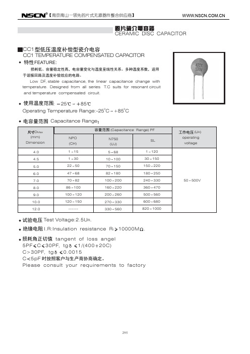
1 15 1 30 22 50 47 68 70 82 86 100 100 120 120 150 ------
5 68 10 100 70 150 82 180 100 200 160 220 200 260 270 330 330 560
1 120 30 150 150 220 180 250 240 330 360 470 500 560 600 680 820 1000
于谐振回路及温度补偿效应的电路。 Low DF, stable capacitance, the linear capacitance change with
temperature. Designed from all series T.C suits for resonant circuit and temperature compensated circuit.
E P
包封形式 环氧包封 酚醛包封
Enciosure style Epoxy resin Phenol resin
11.W- 表示无铅产品 Lead-Free 温度系数 TEMPERATURE CHARACTERISTICS
材料温度系数及允许偏差 :X10-6/ 0 60
750 120 140 1000
2 额定电压 Rated voltage
Letter symbol D
E
F
G
J
K
L
NM P
QR
X
Y
rated voltage 16V 25V 50V 100V 160V 250V 500V 1KV 2KV 3KV 4KV 6KV 250VAC 400VAC
3 电容本体直径 Diameter
代号 symbol
国巨电容命名规则
国巨电容命名规则
国巨电容的命名规则通常遵循以下几个规则:
1. 电容器型号一般由字母和数字组成。
其中,字母代表电容器
的一些特性,比如温度系数、容量稳定度等;数字则表示电容量大小,单位为微法(μF)。
2. 电容器型号的第一个字母通常代表电容器的材料种类。
例如:
- C:钽电容器(tantalum capacitor)
- E:铝电解电容器(aluminum electrolytic capacitor)
- K:多层陶瓷电容器(multilayer ceramic capacitor)
- P:聚酯薄膜电容器(polyester film capacitor)
- N:聚酰亚胺薄膜电容器(polyimide film capacitor)
- S:固体电解电容器(solid electrolytic capacitor)
3. 电容器型号中的其他字母和数字则有可能代表其他一些特性,比如电压、封装规格等。
例如:
- 104:表示电容量为100nF(10的4次方)
- 25V:表示电容器的额定电压为25V
- A/B/C:表示封装规格,不同的字母代表不同的封装方式。
总之,国巨电容的型号中字母和数字的组合代表了电容器的各种
特性,可以根据需要选择合适的型号。
国巨_贴片电容_规格说明-ST_NPOX7R_16V-to-3KV_4
DIMENSION Table 1 For outlines see fig. 3
TYPE L1 (mm) W (mm) T (mm)
0402 0603 0805 1206
1210
1808 1812
1.0 ± 0.15 1.6 ± 0.20 1.6 ± 0.25
0.5 ± 0.15 0.8 ± 0.15 0.8 ± 0.25
force before order.
Surface-Mount Ceramic Multilayer Capacitors
Soft Termination
NPO & X7R
Product specification 3
16V to 3KV
19
CONSTRUCTION
The capacitor consists of a rectangular block of ceramic dielectric in which a number of interleaved metal electrodes are contained. This structure gives rise to a high capacitance per unit volume. The inner electrodes are connected to the two end flexible terminations and finally covered with a layer of plated tin (NiSn). The terminations are lead-free. A cross section of the structure is shown in Fig.1 and Fig.2.