Si基体中掺杂B,P的第一性原理研究
SiC第一性原理的研

LDA
GGA
图6
五、总结
a、由图1可知,在同样的晶胞体积下,用GGA的方法计算单点能比用 LDA方法计算的能量要高6eV左右。随着截断能的增高,总能量最终趋 近于一定值,但随之计算时间会变长。 b、由图4可知,K点精度设置的越高,计算得到的总能量就越趋近于 一个定值,同样计算时间会变长。 c、由图2、3、5可知,用GGA方法计算所需的时间要比用LDA方法 的短。由图6可知,用GGA方法计算的禁带宽度1.394eV要略大于 LDA方法计算的1.346eV,更接近于实验值2.417eV。 由a、b可知计算是精度设置得越高,所得的结果就越精确。但是 由于计算时要考虑到计算效率,所以在计算时要按实际情况进行相 应的设置。对于本次计算,在保证了计算结果精确性的情况下,又 较好的控制了计算时间,所以设置是比较合理的。由c可知对于3CSiC用GGA方法计算能带结构所得的结果会更精确,同时也会更省 时。 综上所述,本次计算结果是可信的,但是用GGA方法计算会更好。
SiC第一性原理的研究
姓名:王涛 专业:材料物理 学号:20111338001
一、SiC晶体
SiC是一种优良的半导体,常见的SiC有4种 结构,分别是3C-SiC(闪锌矿结构)、2H-SiC (铅锌矿结构)、4H-SiC、6H-SiC,本次计算将 采用3C-SiC。 通过查询可知3C-SiC空间群为F-43M,晶格 常数a=b=c=0.43589nm,禁带宽度为2.417eV, 价电子为C:2S2 2P2 ,SiC:3S23P2。
表1、截断能与总能量的对应数据
图1、截断能与总能量的关系
图2、截断能与时间的关系
从图1可以看出,截断能增大到从280eV时,总能量开始收敛, 而初始设定310eV高于280eV,所以认定截断能设为310eV计算 得到的结果是可信的。从图2可以看出,截断能越大,计算所需 时间就越长。所以可以将截断能设定为310eV来测试SCF对总能 量的影响,以减少计算量,和计算时间。
Si中B元素的室温扩散与吸杂现象研究
硅中硼元素的室温扩散与吸杂现象研究谢兮兮导师:秦国刚2015.6Diffusion and Gettering of B Elements in Si at Room TemperatureByXixi XieDirected ByProf.Guogang QinSchool of Physics,Peking UniversityJun.2015摘要半导体材料是制造电子设备不可或缺的材料,在当下的信息化社会里占据尤为重要的地位。
半导体中掺入微量的杂质元素,就会对半导体的物理和化学性质产生决定性影响。
硼元素是半导体中的重要受主杂质,在硅中主要以代位形式存在。
传统改变掺杂在硅中硼的方法是,在高温下通过提高代位硼扩散系数来实现。
本文探讨在室温的条件下,使用高密度等离子体刻蚀机处理硅样品,以实现硼的快速扩散和吸杂,并尝试提出解释的吸杂机制。
关键词:半导体硼元素扩散室温吸杂AbstractSemiconnductor material is fundamental for manufacturing electronic equipment and the development of the information society.The impurity elements which are adulterated in Silicon have an important impact on the physical and chemical properties of semiconductor material.The most common acceptor impurity element, Boron,exists in the form of substitutional impurity.The traditional method of altering Boron element in Silicon is to reach a high temperature.The article will focus on how to alter the Boron element at room temperature with ICP,and give a proper explanation.Keywords:seimiconductor,diffusion of Boron,gettering at room temperature目录第一章引言 (1)第二章硅中浅能级杂质和实验相关设备原理介绍 (2)2.1浅能级杂质的存在方式与基本属性 (2)2.2硅中B、P、As等杂质的扩散与高温吸杂 (4)2.2.1杂质扩散 (4)2.2.2高温吸杂 (6)2.3高密度等离子体刻蚀机运行原理与离子注入简介 (7)2.3.1高密度等离子体刻蚀机 (7)2.3.2离子注入 (8)第三章ICP刻蚀下硅中硼的室温扩散与吸杂机制 (11)3.1实验方法 (11)3.2实验数据与结论 (11)3.3讨论与机制猜测 (14)第四章结论与展望 (20)第一章引言自然界分导体、绝缘体和半导体三类。
Si基体中掺杂B,P的第一性原理研究
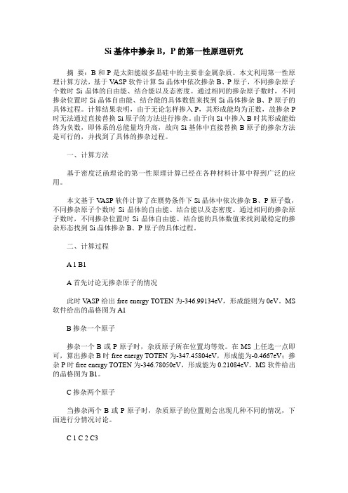
Si基体中掺杂B,P的第一性原理研究摘要:B和P是太阳能级多晶硅中的主要非金属杂质。
本文利用第一性原理计算方法,基于V ASP软件计算Si晶体中依次掺杂B、P原子,不同掺杂原子个数时Si晶体的自由能、结合能以及态密度。
通过相同的掺杂原子数时,不同掺杂位置时Si晶体自由能、结合能的具体数值来找到Si晶体掺杂B、P原子的具体过程。
计算结果表明,由于无论怎样掺入P,其形成能均为正数,故掺杂P 时无法通过直接替换Si原子的方法进行掺杂。
由于向Si中掺入B时其形成能始终为负数,即体系的总能量均升高,故向Si基体中直接替换B原子的掺杂方法是可行的,并找到了具体的掺杂过程。
一、计算方法基于密度泛函理论的第一性原理计算已经在各种材料计算中得到广泛的应用。
本文基于V ASP软件计算了在赝势条件下Si晶体中依次掺杂B、P原子数,不同掺杂原子个数时Si晶体的自由能、结合能以及态密度。
通过相同的掺杂原子数时,不同掺杂位置时Si晶体自由能、结合能的具体数值来找到最稳定的掺杂形态找到Si晶体掺杂B、P原子的具体过程。
二、计算过程A 1 B1A首先讨论无掺杂原子的情况此时V ASP给出free energy TOTEN为-346.99134eV,形成能则为0eV。
MS 软件给出的晶格图为A1B掺杂一个原子掺杂一个B或P原子时,杂质原子所在位置均等效。
在MS上任选一点即可,算出掺杂B时free energy TOTEN为-347.45804eV,形成能为-0.4667eV;掺杂P时free energy TOTEN为-346.78050eV,形成能为0.21084eV。
MS软件给出的晶格图为B1。
C掺杂两个原子当掺杂两个B或P原子时,杂质原子的位置则会出现几种不同的情况,下面进行分情况讨论。
C 1 C 2 C3如图C1,由V ASP算得掺杂B时free energy TOTEN为-347.412888eV,形成能为-0.421548eV;掺杂P时free energy TOTEN为-346.353895eV,形成能为0.637445eV。
磷酸铁锂正极材料掺杂改性的第一性原理研究

磷酸铁锂正极材料掺杂改性的第一性原理研究磷酸铁锂正极材料掺杂改性的第一性原理研究磷酸铁锂(LiFePO4)作为一种重要的正极材料,由于其高能量密度、较低的材料成本和良好的循环稳定性而备受瞩目。
然而,其相对较低的离子导电性和电子导电性限制了其在电池中的应用效能,限制了其在高功率需求下的使用。
因此,在研究中如何提高磷酸铁锂正极材料的电化学性能是一个重要的课题。
掺杂是一种有效的手段,可以改善材料的电化学性能。
通过向磷酸铁锂正极材料中引入其他元素,可以调节材料的电子结构、改善电子传输和离子扩散,从而提高其电化学性能。
因此,本文通过第一性原理计算方法,研究了不同掺杂元素对磷酸铁锂正极材料性能的影响。
首先,我们选取了几种常用的掺杂元素,包括锌(Zn)、镍(Ni)、钴(Co)和锑(Sb),分别将它们掺杂到磷酸铁锂结构中,并对其进行优化计算。
通过计算发现,这些掺杂元素可以有效地改变磷酸铁锂正极材料的电子结构。
例如,锌和镍的掺杂可以减小能隙,增加导电性;钴的掺杂可以提高材料的离子扩散速率;锑的掺杂可以改善材料的结构稳定性。
其次,我们进一步研究了不同掺杂浓度对磷酸铁锂材料性能的影响。
通过计算发现,适量的掺杂可以提高材料的电化学性能,但过高或过低的掺杂浓度则可能导致材料性能下降。
因此,寻找合适的掺杂浓度是非常重要的。
最后,我们对掺杂元素的位置进行了研究。
我们发现,不同掺杂位置对材料的性能有很大的影响。
例如,在磷酸铁锂材料的龙骨结构中,掺杂元素可以替换铁原子或磷原子,从而改变材料的结构和导电性。
在掺杂过程中,掺杂元素与其他原子之间的相互作用也起着关键的作用。
综上所述,通过第一性原理计算方法,我们系统地研究了不同掺杂元素对磷酸铁锂正极材料性能的影响。
这些研究结果可以为进一步优化磷酸铁锂正极材料的性能提供理论指导,为新型电池的设计和应用提供重要的参考。
然而,由于复杂的电化学反应和体系的多变性,还需要进一步的实验研究来验证并完善这些理论模拟结果。
Nb掺杂影响NiTi金属间化合物电子结构的第一性原理计算

图@
!! 构型 C-&- ! K ! K ! 超晶胞模型 图! 掺杂 C+ 原子前后 !! C-&- 合金中的各点缺陷生成能对比图
= " 计算结果和讨论
!"#" $% 原子对 ! & $’(’ 点缺陷生成能的影响 在 C-&- 高温氧化过程中, C- 原子和 &- 原子的
合金生成前后总能量的变化, 即 (C-@L ’ L ( &- ( C+ ’ )N ) (C-@L ’ L ( &- ( C+ ’ ) "& (C-) L(@ L ’ L ( )K ) ( &-)L ’) (C+) ,(!) L () (C-I"H &-I"H )N ) (C-I"H &-I"H )L I"H ) (C-) "&
[!!, !=] 计算的理论方法 8 本文中电子与电子间相互作
产生 C- 和 &- 原子点缺陷则是原子扩散过程进行的 前提条件 8 理想的 ! ! C-&- 结构属于体心立方结构, 是由 C- 原子和 &- 原子分别占据体心原子与顶角原 子 8 在实际应用中, 因 C-&- 结构往往偏离理想结构, 而产生点缺陷 8 在纯 C-&- 中存在 C- 原子和 &- 原子 晶格位置的空位点缺陷和反位点缺陷 8 当添加合金 在纯 C-&- 结 化元素后, 还存在取代位置缺陷 8 因此, 即 C- 空位, 构中, 存在 B 种基本的单点缺陷类型, &空位, 反位 ( 占据 位置) , 反位 ( 占据 CC&&&C位置) , 分别标记为 % C- ,% &- , 当添加 C+ 元 C-&- , &-C- ; 素后, 除了上述 B 中点缺陷外, 还有 C+ 取代 &- 或者 标记为 C+&- 和 C+C- 8 点缺陷生成 C- 所形成的点缺陷, 能 ( &. ) 是衡量点缺陷生成难易程度的一个重要指 本论文只 标 8 由于多个点缺陷并存的情况比较复杂, 对单点缺陷 % C- ,% &- ,C-&- , &-C- , C+&- 和 C+C- 的生成能 进行研究, 根据文献 [!H—!P] , 点缺陷生成能 ( &. ) 定义为 "& N "& . L "& C-&- , (@) &. N ! ’. !’ . 其中, "& . 是含有点缺陷的 ! ! 构型 C-&- 体系的形 成能, "& C-&- 是理想 ! ! C-&- 体系的形成能,’ . 为点 缺陷的原子浓度 8 在本文中, 对于取代点缺陷 &-C- , 由于超晶胞中原子总数为 @F, C-&- ,C+&- ,C+C- 来讲, 因此, 单个点缺陷的原子浓度为 ’ . N @M@F 8 而对于空 位缺陷 % C- 和 % &- 来讲, 由于产生一个空位后, 超晶胞 中原子总数变为 @H, 因此, 单空位点缺陷的原子浓 度为 ’ . N @M@H 8 C-&-9C+ 和 C-&- 体系的形成能定义为
第一性原理研究Pt掺杂NiTi金属间化合物晶体结构与电子结构

第一性原理研究Pt掺杂NiTi金属间化合物晶体结构与电子结构别业旺;孙卫国【摘要】利用第一性原理研究了Pt掺杂B2结构的NiTi合金的晶体结构与电子结构.研究表明,Pt掺杂比例不高于6.25%时,体系的结构不发生变化,并且点缺陷形成能更低,说明掺杂Pt元素能提高体系的稳定性.而态密度,布局分析以及电荷密度分布的计算进一步表明,Pt原子的d电子成键能力很强,与周围原子剧烈的相互作用,结构更为稳定.通过比较不同取代位点得出Pt更倾向于取代Ni位.【期刊名称】《西南民族大学学报(自然科学版)》【年(卷),期】2011(037)004【总页数】6页(P647-652)【关键词】NiTi金属间化合物;Pt掺杂;电子结构【作者】别业旺;孙卫国【作者单位】四川大学原子与分子物理研究所四川成都610065;四川大学原子与分子物理研究所四川成都610065【正文语种】中文【中图分类】O56Due to the excellent shape memory effect and super elastic behavior, NiTi intermetallic compound, is widely applied in many fields, such asautomation, aerospace and biomedical science [1-3]. Moreover, because alloying element plays an important role in controlling the martensite transformation temperature or modifying crystalline structure, the NiTi-based ternary alloys are also gained more and more attentions, such as Ni-Ti-Hf, Ni-Ti-Cu, Ni-Ti-Zr, Ni-Ti-Nb, Ni-Ti-Al,Ni-Ti-Mn, Ni-Ti-Pt and Ni-Ti-Pd[4-12]. However, almost all of these alloying elements will increase the Matensite transformation temperature and it is a disadvantage for applying the pseudoelastic properties of NiTi on medicaldevices.Fortunately, there exits an exception that Pt (with additions of 0-10 at.%) can decrease the transformation temperature of NiTi alloy[13]. In addition, NiTiPt alloys demonstrate a much smaller stress hysteresis and smaller temperature dependence of transformation stress comparing to NiTi alloys, with the strength and ductility of NiTiPt and NiTi alloys are basically identical [13]. Therefore, the NiTiPt alloy is a potential material for medical devices and thus many researches is concentrated on this material. In this paper, the crystalline structure, site preference, electronic structure and bonding behavior of Pt-doped NiTi intemetallic compound are investigated by using the first principle method.The calculations presented in this study are performed with the Cambridge Serial Total Energy Package[14-15](CASTEP), based on the density functional theory, using Vanderbilt-type ultrasoft pseudopentials[16] and a plane-wave expansion of the wave functions. We use the generalized gradient approximation (GGA) in the scheme of Perdew-Wang[17] (PW91) to describe the exchange and correlation potential. The structure isoptimized with the Broyden-Fletcher-Goldfarb-Shanno method[18]. The plane-wave cutoff energy of 500 eV is employed. The k-mesh is setto be 8×8×8 Monkhorst-Pack grid. The convergence is assumed when the forces on atoms are less than 0.03eV/ Å. The self-consistence convergence of energy is set to 1×10⁻⁶ eV/atom, and the displacement tolerance is set to be 0.0002nm while the stress diviation is with the value of 0.1 GPa. All necessary convergence tests are performed to be reliable.Structure of B2-NiTi is composed of Ni and Ti cubic sublattices, and the Ni and Ti atoms are commutable because of geometrical symmetry[19]. In this paper, we create a structure named Ni8Ti8 (2×2×2 supercell of NiTi,a=b=c=6.028,α=β=γ=90°, shown in Fig.1. a). With the center atom (Ni or Ti) of Ni8Ti8 replaced by Pt atom, the Pt-doped NiTi alloy crystal lattice structures (Ni8Ti7Pt and Ni7Ti8Pt, shown in Fig.1.(b) and (c)) are constructed. So the doping concentration in our model is set to be 6.25 at%, and this value is in the range of most of theoretical and experimental study [11,13].3.1 Crystal structureThe fully relaxed equilibrium lattice constants and other theoretical or experimental results are listed in Table.1.Ni8Ti8 is still cubic, as shown in Table.1. The calculated a=6.041nm, which is in good agreement with the experimental and other theoretical value[20,23]. Ni8Ti7Pt and Ni7Ti8Pt still retain initial cubic structures, which mean that Pt doping may not change the cubic structure of NiTi system under the doping concentration of6.25%. For the optimized Ni8Ti7Pt,the lattice constants are slightly smallerthan that of Ni8Ti8. However, the calculated lattice constants of Ni7Ti8Pt are larger than that of Ni8Ti8. These results indicate that different substitution sites (PtTi and PtNi) bring about the difference in the change trend of lattice constants.3.2 Formation energyThe formation energy (Ef) is a key issue to estimate the difficulty of the formation of point defect[24]. In this work,two kinds of points caused by different Pt substitution (named as PtNi and PtTi), are studied in detail. The formation energy is defined as followWhere EtNixTiyXz is the total energy of X-doped supercell, and ENibulk, ETibulk, EXbulk are the total energy of the fcc Ni, hcp Ti and fcc Pt, respectively. The formation energy of the three supercells is listed in Table 1. It is obviously that both Ni8Ti7Pt and Ni7Ti8Pt have smaller Ef compared to Ni8Ti8, indicating that Pt dopant will strengthen the stability of NiTi alloy. Furthermore, as the lower formation energy of Ni7Ti8Pt is, it can be inferred that Pt is likely to occupy Ni site in Ni8Ti8 crystal lattice.3.3 Density of statesAs the addition of Pt, the geometrical structure has changed, and the electrical structure varies correspondingly. In this work, the consequence of Pt doping in NiTi is investigated qualitatively by partial density of states (PDOS) of each atom. The 5d electron occupied absolutely all the electron configuration of Pt, meaning that the 5d electron made almost all the contribution of electronic structure of Pt atom. As to Ni atom, we only analysis the 3d electrons because of the contribution of s and p electronsis negligible. In our discussion, we plan to discuss the s and p electron of Ti atoms at first, and then focus on the d electrons of the three elements in NiTi alloy.The PDOS of s electron of Ti atom is shown on the top of Fig.2, while the p electron of that is shown at the bottom.The line of Ni7Ti8Pt is nearly the same with that of Ni8Ti8, while the peak of the Ni8Ti7Pt line is lower than the original Ni8Ti8, both in the two part of Fig.2. The results only meant to show that the contribution of s and p electron of Ti atom are reduced by the Pt substituting central Ti atom, but have no change when Pt substitutes central Ni atom.The PDOS of d electron of each atom are shown in detail in Fig.3, top panel for Ti-d PDOS, middle panel for Ni-d PDOS, and bottom panel for Pt-d PDOS. For the Ti-d PDOS, the line of Ni8Ti7Pt moves away from Fermi energy, while the line of Ni7Ti8Pt keeps the same with Ni8Ti8. For the Ni-d PDOS, the lines of Ni8Ti7Pt and Ni7Ti8Pt move downward,comparing with that of Ni8Ti8. Furthermore, the line of Ni8Ti7Pt drops deeper. It can be inferred that the d PDOS of Ni and Ti atom will be weaken significantly with the Pt substitution for Ti, but stay the same as the Pt substituting for Ni.For the Pt-d PDOS, the line of Pt does not appear any obvious peak in the hexagonal Pt, but presents strong peaks near the Fermi energy as the alloying element in NiTi intermetallic compound. Furthermore, the line of Ni7Ti8Pt has the higher and narrower peaks than that of Ni8Ti7Pt. Drawn by these discoveries, it is no doubt that the Pt has strong interaction with Ni or Ti atoms due to the d electrons, and this interaction behaves moreintensive in Ni7Ti8Pt.To summarize the discussion mentioned above, we point out that, different sites of substitution result in different influence on the electron structure, and the Pt prefers to substitute Ni site. In a word, it is possible that the PtNi will dominate the doping behaviors.3.4 Population analysisIn order to reveal the influence of Pt doping on the electron structure of NiTi supercell for further, we obtain the Milliken population of the centre atom and its nearest neighbor atoms, and then analyze the charge gain or loss behaviors. Table 2 lists the results of Milliken population, indicating that the Pt doping changed the charge distributions of each atom at different levels. For the Ni8Ti8, the Ni atom gains 0.33 , as the Ti atom lost the equal charge, which means that bonding is dominant in the electronic interactions. As to the Ni8Ti7Pt, Ni and Pt atom have minus charge,and manifest gaining charge, and then resulting in competition between them. For the Ni7Ti8Pt, the charge of Pt and Ti has opposite sign. Furthermore, the charge of the Pt atom is with the value of -1.09, meaning that the Pt has very strong ability of gaining electrons. From the discussion above, it is inferred that the substitution of central Ni atom for a Pt atom can enforce the bonding interactions.3.5 Electron densityElectron density provides additional information regarding the consequences of the detailed electron structure described above. Fig.4 plot the density electron of (110) plane of each structure. As see in thisfigure, there is the hybridization between the Ni(Pt) and Ti(Pt) atoms. However, the charge density around Ni and Ti atoms is lower and more localized than that around Pt atoms. Therefore, the hybridization between the Pt and Ti(Ni) is stronger than that between the Ti and Ni atoms. Moreover, the hybridization between Pt and Ti atoms is stronger than that between the Pt and Ni atoms, indicating that PtNi is more stable.In this work, we implement the first principle calculation to determine the structure stability and electron structure properties of NiTi intermetalic compound with or without Pt doping. The formation energies of bothNi8Ti7Pt and Ni7Ti8Pt rose, indicating that the NiTi alloy manifests more stable after Pt doping. The results of partial density of states,Milliken population and electron density analysis demonstrate that the Pt atom prefers to replace the Ni atom.【相关文献】[1] WEVER D J, VELDHUIZEN A G , VERIES J DE, et al. Electrochemical and surface characterization of a nickel–titanium alloy[J].Biomaterials, 1998, 19: 761-769.[2] RUTA R S, GADIYAR A S, MADANGOPAL K et al. Biocompatibility of Ni-Ti shape memory alloy[J]. Corrosion,1993, 28:217-221.[3] THIERRY B, TABRIZIAN M, TREPANIER C, et al. Effect of surface treatment and sterilization processes on the corrosion behavior of NiTi shape memory alloy[J]. J Biomed Mater Res, 2000,51: 685-693.[4] LI C B, LI M K, YIN D, et al. First principles study on the charge density and the bulk modulus of the transition metals and their carbides and nitrides[J]. Chin Phys, 2005, 14: 2287-2292.[5] XU X G , WANG C Z, LIU W, et al. Ab initio study of the effects of Mg doping on electronic structure of Li (Co, Al) O2[J]. Acta Phys Sin, 2005, 54: 313-316.[6] WU H LI, ZHAO X Q, GONG S K. Nb掺杂影响NiTi金属间化合物电子结构的第一性原理计算[J]. Acta Phys Sin, 2010, 59:515-520.[7] K OTSUKA, X REN. Physical metallurgy of Ti-Ni-based shape memory alloys[J]. Progress in Materials Science, 2005, 50: 511-678.[8] SANJABI S, CAO Y Z, BARBER Z H. Multi-target Sputter Deposition of High Temperature Shape Memory Ni50Ti50-xHfx Thin Films[J]. Sens Actuators A, 2005, 121: 543-548.[9] BERTHEVILLE B. Powder metallurgical processing of ternary Ni50Ti50−xZrx(x = 5, 10 at.%) alloys[J]. J Alloys Compd, 2005,398:94-99.[10] XU Y, SHIMIZU S, SUZUKI Y, et al. Recovery and recrystallization processes in Ti---Pd---Ni high-temperature shape memory alloys [J].Acta Mater,1997, 45: 1503-1511.[11] MOHANCHANDRA K P, SHIN D, CARMAN G P. Deposition and characterization of Ti-Ni-Pd an Ti-Ni-Pt shape memory alloy thin films[J]. Smart Mater Struct, 2005, 14: S312-S316.[12] MOSCA H O, BOZZOLO G, GROSSO M F DEL. Thermal and physical properties of Al-Ni-Ru-M alloys[J]. Intermetallics,2009,162: 99-105.[13] LIN B, GALL K, MAIER H J, WALDRON R. Structure and thermomechanical behavior of NiTiPt shape meomory alloy wires[J].Acta Biomaterialia,2009,5: 257-267.[14] KEIJI W, MASATOSHI S, HIDEAKI T, et al. Formation of composite oxide films on Aluminum by Sol-Gel coating and anodizing-For the development of high performance Aluminum electrolytic capacitors[J].Electrochemistry ,2001, 69: 407-413.[15] KEIJI W, MASATOSHI S, HIDEAKI T. Foramtion of Al-Zr composite oxide films on aluminum by sol-gel coating and anoding[J].J Electroanal Chem, 1999, 473: 250-255. [16] Vanderbilt D. Soft self-consistent pseudopotentials in a generalized engenvalue formalism[J].Phys Rev B, 1990, 41: 7892-7895.[17] PERDEW J P, CHEVARY J A, VOSKO S H, et al. Atoms, molecules, solids, and surfaces: Applications of the generalized gradient approximation for exchange and correlation[J]. Phys Rev B, 1992, 46: 6671-6687.[18] PFROMMER B G, COTE M, LOUIE S G et al. Relaxation of crystals with the Quasi-Newton Method[J]. J Comput Phys, 1997, 131:133-140.[19] GOO E, SINCLAR R. The B2 to R transformation in Ti50Ni47Fe3 and Ti49.5Ni50.5 alloys[J]. Acta Metall, 1985,33: 1717-1723.[20] HATCHER N, KONTSEVOI Y, FREEMAN A J. Matensitic transformation path ofNiTi[J].Phys Rev B, 2009,79 020202(R).[21] GACHON J, NOTIN M, HERTZ J. The enthalphy of mixing of the intermediate phase in the systems FeTi,CoTi, and NiTi by direct reaction calorimetry[J]. Thermochim Acta, 1981, 48:155-164.[22] HATCHER N, KONTSEVOI O YU, FREEMAN A J. Role of elastic and shear stabilities inthe martensitic transformation path of NiTi[J]. Phys Rev B, 2009, 80: 144203-144220. [23] LU J M, HU Q M, YANG positon-dependent elastic properties and electronic structures of off-stoichiometric TiNi from first-principles calculations[J]. Acta Materialia , 2008,56: 4913-4920.[24] 尚家香, 喻显扬. 3d过渡金属在NiAl中的占位及对键合性质的影响[J]. 物理学报,2008,57:2380-2385.。
碳主族元素掺杂硅的第一性原理计算

碳主族元素掺杂硅的第一性原理计算作者:卜琼琼来源:《科技视界》 2015年第16期卜琼琼(云南机电职业技术学院,云南昆明 650203)【摘要】单晶硅的性质对所含杂质与缺陷十分敏感。
于是,为了在硅上获得适合于实际应用的光发射,人们对Si材料的改性主要采取引入与控制杂质和缺陷的方法,期望获得有效的发光中心,近年来,Si材料的掺杂改性在实验和理论上都获得了广泛的关注。
本文通过第一性原理的方法计算在硅中掺入C、Si、Ge、Sn、Pb等第四主族元素,来对它们的性质进行计算模拟,为Si的掺杂改性做理论分析指导。
【关键词】C族元素;Si;能带;态密度构造2x2x1共32个原子的超晶胞,其中浅色原子代表Si原子,深色原子代表C族(C、Ge、Sn、Pb)元素原子。
采用基于密度泛函理论(Density Functional Theory,DFT)结合平面波赝势方法的CASTEP软件包完成。
电子与电子之间的相互作用通过广义梯度近似(GGA)的PBE的计算方案来处理。
本文采用超软赝势(Ultra-soft pseudopotentials,Usp)描述离子实与价电子之间的相互作用势。
系统总能量和电荷密度在布里渊区的积分计算使用Monkhorst-Pack方案来选择k空间网格点,布里渊区k矢的选取为666,平面波截断能Ecut设为200eV。
经过参数优化,以上参数满足计算要求。
在分析中采用如下的局域轨道作为价轨:C 2s22p2、Si 3s2 3p2、Ge 4s2 4p2、Sn5s2 5p2、Pb 5d10 6s2 6p2。
为了得到体系的稳定结构,在Si实验晶格常数值附近对原胞体积和总能量进行优化。
通过计算不同掺杂原子原胞体积下的体系总能量,得出了Si晶体晶格常数a,b,c。
表1是Si正交相结构优化后的晶格常数。
由表1可看出,几何优化后得到的理论原胞参数与实验值比较接近,误差在1%,与实验值较相近。
对超晶胞进行原子替代,用第四主族元素原子分别取代体系中等同位置的一个Si原子,构成Si31X1体系(X分别为C、Si、Ge、Sn、Pb原子)。
Si-P掺杂石墨烯的稳定性和能带结构的理论研究
墨 烯 结 构 的 形 成 能 较 低 ,比 较 稳 定 Q S i 掺 杂 石 墨 烯 的 能 带 结 构 在 G 点 产 生 了 约 0 .1 e V 的 带 隙 ,从 良 导 体 过 渡 到 了 半 导 体 Q
在 P 或 S i - P 掺 杂 石 墨 烯 体 系 中 ,费 米 能 级 上 升 而 穿 过 价 带 ,使 掺 杂 系 统 保 持 金 属 性 。态 密 度 计 算 表 明 ,P 或 S i - P 掺杂石
1 计算方法
计 算 主 要 采 用 基 于 紧 束 缚 密 度 泛 函 计 算 方 法 的 D F T B 软 件 包 。紧 束 缚 密 度 泛 函 计 算 方 法 对 交 换 积 分 进 行 近 似 和 参 数 化 ,紧 束 缚 近 似 简 化 后 的 哈 密 顿 矩 阵 元 由 电 荷 自 洽 决 定 ,是 一 种 半 经 验 的 计 算 方 法 ,并且 计算速度很高,可以计算较大体系[8]。计 算 中 C、S i 和 P 赝 势 选 择 matsci,自洽场迭代使用简约布里渊区的 2 x 2 x 2 的 [ 点 ,自洽迭代的收敛精度为10-5eV〇计 算 的石墨烯模型为6 x 6 的结构,共 7 2 个 原 子 ,平面
作者简介:牛 群 磊 (1994一 ),男 ,河 南 洛 阳 人 ,在 读 本 科 ,主 要 从 事 低 维 半 导 体 材 料 设 计 与 研 究 。
通讯作者: 朱 伟 玲 (1965— ),女 ,广 东 高 州 人 ,硕 士 ,教 授 ,主 要 从 事 光 电 子 技 术 及 低 维 半 导 体 材 料 性 质 研 究 。
墨 烯 体 系 中 费 米 能 级 附 近 主 要 由 P 原 子 的 3P 态 电 子 和 C 原 子 的 2P 态 电 子 占 据 ,主 要 的 电 子 性 质 与 P 的 3 键 词 :掺 杂 石 墨 烯 ; 紧 束 缚 密 度 泛 函 ;稳 定 性 ;能带结构
- 1、下载文档前请自行甄别文档内容的完整性,平台不提供额外的编辑、内容补充、找答案等附加服务。
- 2、"仅部分预览"的文档,不可在线预览部分如存在完整性等问题,可反馈申请退款(可完整预览的文档不适用该条件!)。
- 3、如文档侵犯您的权益,请联系客服反馈,我们会尽快为您处理(人工客服工作时间:9:00-18:30)。
Si基体中掺杂B,P的第一性原理研究
摘要:B和P是太阳能级多晶硅中的主要非金属杂质。
本文利用第一性原理计算方法,基于V ASP软件计算Si晶体中依次掺杂B、P原子,不同掺杂原子个数时Si晶体的自由能、结合能以及态密度。
通过相同的掺杂原子数时,不同掺杂位置时Si晶体自由能、结合能的具体数值来找到Si晶体掺杂B、P原子的具体过程。
计算结果表明,由于无论怎样掺入P,其形成能均为正数,故掺杂P 时无法通过直接替换Si原子的方法进行掺杂。
由于向Si中掺入B时其形成能始终为负数,即体系的总能量均升高,故向Si基体中直接替换B原子的掺杂方法是可行的,并找到了具体的掺杂过程。
一、计算方法
基于密度泛函理论的第一性原理计算已经在各种材料计算中得到广泛的应用。
本文基于V ASP软件计算了在赝势条件下Si晶体中依次掺杂B、P原子数,不同掺杂原子个数时Si晶体的自由能、结合能以及态密度。
通过相同的掺杂原子数时,不同掺杂位置时Si晶体自由能、结合能的具体数值来找到最稳定的掺杂形态找到Si晶体掺杂B、P原子的具体过程。
二、计算过程
A 1 B1
A首先讨论无掺杂原子的情况
此时V ASP给出free energy TOTEN为-346.99134eV,形成能则为0eV。
MS 软件给出的晶格图为A1
B掺杂一个原子
掺杂一个B或P原子时,杂质原子所在位置均等效。
在MS上任选一点即可,算出掺杂B时free energy TOTEN为-347.45804eV,形成能为-0.4667eV;掺杂P时free energy TOTEN为-346.78050eV,形成能为0.21084eV。
MS软件给出的晶格图为B1。
C掺杂两个原子
当掺杂两个B或P原子时,杂质原子的位置则会出现几种不同的情况,下面进行分情况讨论。
C 1 C 2 C3
如图C1,由V ASP算得掺杂B时free energy TOTEN为-347.412888eV,形成能为-0.421548eV;掺杂P时free energy TOTEN为-346.353895eV,形成能为0.637445eV。
如图C2,由V ASP算得掺杂B时free energy TOTEN为-347.920743eV,形成能为-0.929403eV;掺杂P时free energy TOTEN为-346.484889eV,形成能为0.506451eV。
如图C3,此时由V ASP算得掺杂B时free energy TOTEN为-348.059883eV,形成能为-1.068543eV;掺杂P时free energy TOTEN为-346.538671eV,形成能为0.452669eV。
D掺杂三个原子
当掺杂三个B或P原子时,杂质原子的位置则会出现几种不同的情况。
D 1 D2
如图D1,由V ASP算得掺杂B时free energy TOTEN为-347.042041eV,形成能为-0.050701eV;而掺杂P时free energy TOTEN为-345.82922eV,形成能为1.16212eV。
如图D2,由V ASP算得掺杂B时free energy TOTEN为-347.677310eV,形成能为-0.68597eV;掺杂P时free energy TOTEN为-346.08004eV,形成能为0.91130eV。
E掺杂四个原子
E 1 E2 E3
如图E1,由V ASP算得掺杂B时free energy TOTEN为-346.636095eV,形成能为0.355245eV;而掺杂P时free energy TOTEN为-345.515436eV,形成能为1.475904eV。
如图E2 ,由V ASP算得掺杂B时free energy TOTEN为-347.145871eV,形成能为-0.154531eV;掺杂P时free energy TOTEN为-345.468484eV,形成能为1.522856eV。
如图E3,由V ASP算得掺杂B时free energy TOTEN为-346.470160eV,形成能为0.52118eV;掺杂P时free energy TOTEN为-345.394398eV,形成能为1.596942eV。
F掺杂五个原子
F 1 F2 F3
如图E1,由V ASP算得掺杂B时free energy TOTEN为-346.087825eV,形成能为0.903515eV;掺杂P时free energy TOTEN为-344.943658eV,形成能为2.047682eV。
如图E2,掺杂B时free energy TOTEN为-347.337625eV,形成能为-0.346285eV;掺杂P时free energy TOTEN为-345.204567eV,形成能为1.786773eV。
如图E3,掺杂B时free energy TOTEN为-346.491222eV,形成能为0.500118eV;掺杂P时free energy TOTEN为-345.077092eV,形成能为1.914248eV。
G掺杂六个原子
G 1 G2 G3
如图G1,由V ASP算得掺杂B时free energy TOTEN为-344.926872eV,形成能为2.064468eV;掺杂P时free energy TOTEN为-344.078754eV,形成能为2.912586eV。
如图G2,由V ASP算得掺杂B时free energy TOTEN为-346.986191eV,形成能为0.005149eV;掺杂P时free energy TOTEN为-344.756896eV,形成能为2.234444eV。
如图G3,由V ASP算得掺杂B时free energy TOTEN为-347.218160eV,形成能为-0.22682eV;掺杂P时free energy TOTEN为-344.614332eV,形成能为2.377008eV。