缓冲电路笔记
缓冲电路

主要应用
各种直流电源,如蓄电池、干电池、太阳能电池等。 交流电机调速用变频器、不间断电源、感应加热电源 等电力电子装臵的核心部分都是逆变电路。
换流方式
• 逆变电路的基本工作原理
• 换流方式分类
逆变电路的基本工作原理
以单相桥式逆变电路为例说明最基本的工作原理
S1~S4是桥式电路的4个臂,由电力电子器件及辅 助电路组成。
电压型逆变电路
1)逆变电路的分类 —— 根据直流侧电源性质的不同
直流侧是电压源
电压型逆变电路——又称为电压源
型逆变电路 Voltage Source Type Inverter-VSTI
直流侧是电流源
电流型逆变电路——又称为电流源
型逆变电路 Current Source Type Inverter-CSTI
单相电压型逆变电路
1)单相半桥逆变电路
工作原理
V1和V2栅极信号在一周期内 各半周正偏、半周反偏,两 者互补,输出电压uo为矩形 波,幅值为Um=Ud/2。
V1或V2通时,io和uo同方向, 直流侧向负载提供能量; VD1或VD2通时,io和uo反向, 电感中贮能向直流侧反馈。 VD1、VD2称为反馈二极管, 它又起着使负载电流连续的 作用,又称续流二极管。
参数计算与器件选择
根据不同的负载类型计算负载等效阻抗: 电阻型:Z=R 电阻电感型:Z=R+jωL Z=(R2+(ωL)2 ) ½ 对于RLC:Z=R+jωL-1/jωC 对于电阻:i=2P/Ud=Ud/2R 对于电阻电感:i=2P/Udcosφ=Ud/2Z 开关管上的电压:U=(2~3)Ud 电流:I=(1.5~2)(2)1/2i
电阻负载时,负载电流 io 和uo的波形相同,相位也 相同。
IGBT缓冲电路总结
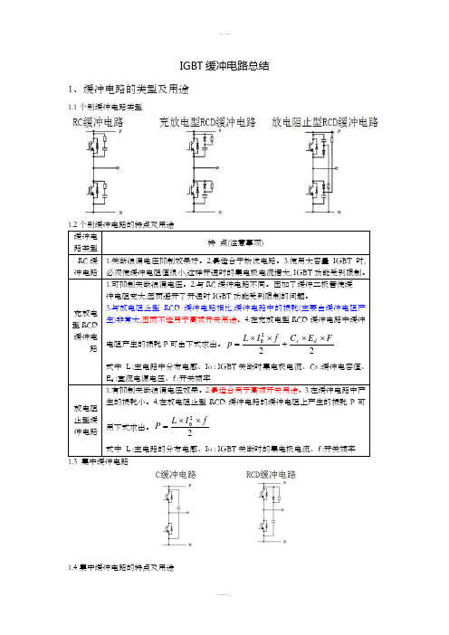
IGBT缓冲电路总结1、缓冲电路的类型及用途1.1个别缓冲电路类型缓冲电路类型特点(注意事项)RC缓冲电路1.关断浪涌电压抑制效果好。
2.最适合于斩波电路。
3.使用大容量IGBT时,必须使缓冲电阻值很小,这样开通时的集电极电流增大, IGBT功能受到限制。
充放电型RCD缓冲电路1.可抑制关断浪涌电压。
2.与RC缓冲电路不同。
因加了缓冲二极管使缓冲电阻变大,因而避开了开通时IGBT功能受到限制的问题。
3.与放电阻止型RCD缓冲电路相比,缓冲电路中的损耗(主要由缓冲电阻产生)非常大,因而不适用于高频开关用途。
4.在充放电型RCD缓冲电路中缓冲电阻产生的损耗P可由下式求出。
222FECfILp ds⨯⨯+⨯⨯=式中L :主电路中分布电感、Io : IGBT关断时集电极电流、Cs :缓冲电容值、E d :直流电源电压、f :开关频率放电阻止型缓冲电路1.有抑制关断浪涌电压效果。
2.最适合用于高频开关用途。
3.在缓冲电路中产生的损耗小。
4.在放电阻止型RCD缓冲电路的缓冲电阻上产生的损耗P可用下式求出。
22fILP⨯⨯=式中L :主电路的分布电感、Io : IGBT关断时的集电极电流、f :开关频率1.3 集中缓冲电路1.4集中缓冲电路的特点及用途以RCD 缓冲吸收电路为例,其中应用的元件需要结合实际的情况进行选择。
其中的吸收电容Cs 的选择可以采用下面的公式:()2020c pk s s U U I L C -= 电路中的电阻Rs 不宜过大,如太大Cs 放电时间过长,电不能完全放掉。
但Rs 太小,在器件导通时,RsCs 放电电流过大、过快,可能危及器件的安全,也可能引起振荡。
一般的,电阻选择参考下面的公式:sws s f C R ⨯=61 其中,LS :主电路电感,主要是没有续流时的杂散电感;Upk :C S 上的最大充电电压; U C0:电源电压;Io :负载电流;f sw :开关频率。
需要注意的是,电容应该选择无感电容;电阻要注意它的功耗,应选择相应的功率电阻;吸收模块的制作要注意绝缘。
塞米控应用笔记 IGBT测量和缓冲电容规格

Application Note Revision: Issue Date: Prepared by: 002008-03-17Joachim Lamp Key Words: IGBT module, snubber capacitor, peak voltage IGBT Peak Voltage Measurement and Snubber Capacitor SpecificationGeneral.................................................................................................................................................................1 Capacitor parameter.............................................................................................................................................2 DC voltage class...................................................................................................................................................2 Capacitance and series-inductance .....................................................................................................................2 Pulse handling......................................................................................................................................................3 RMS voltage and RMS current.............................................................................................................................3 Lifetime.................................................................................................................................................................3 Measurements and verification.............................................................................................................................3 Voltage stress of IGBT (V CEpeak )............................................................................................................................3 Measuring capacitor RMS current........................................................................................................................5 Temperature and self heating under operation....................................................................................................7 Symbols and terms used.. (7)This application note provides information on how to select and test snubber capacitors for IGBT modules in high power applications and how to test the effectiveness. This information should help to prevent failure of the IGBT module and snubber capacitor caused by electrical or thermal overstress. The information given in this application note contains tips on which parameter of the capacitor should be considered and how to carry out the necessary measurements.GeneralIf high currents are switched fast, then voltage overshoots occur, which can destroy the switching power semiconductor. The voltage overshoot is caused by the energy stored in the magnetic field of the current path (e.g. DC-link connections). It is linked by the value of the parasitic inductance or stray inductance L S (E=0,5*L S *i²). The voltage (V=LS *di/dt) may exceed the maximum blocking voltage of the power semiconductor (V CES , V RRM …) because it is added to the DC-link voltage. The first countermeasure is a good low inductive DC-link design to keep the voltage on the semiconductor low. This is done by means of a laminated bus bar system (sandwich of +DC, –DC metal sheets and an insulation layer between) and short connections between the voltage source (DC-link capacitor) and power semiconductor. In addition, snubber capacitors are recommended, which should be mounted directly on the DC-link terminals of each IGBT module. This snubber works as a low-pass filter and “takes over” the voltageovershoot. Fig. 1 shows typical designs. The waveform in Fig. 2 shows in comparison the voltage across an IGBT at turn-off with and without snubber capacitor. The effect of voltage spike reduction can be seen clearly. Fig. 3 shows an equivalent circuit with parasitic inductances.Fig. 1 Low inductance snubber capacitors for mounting on IGBT modulesApplication Note AN-7006In order to decide whether a snubber capacitor is necessary, the maximum collector-emitter voltage (V CEpeak ) of the IGBT has to be checked under worst case conditions to be sure that V CES will not be exceeded under any operating condition. If necessary, several aspects have to be considered when choosing the right snubber capacitor for the application:1. Capacitor DC-voltage class.2. Capacitance value and series inductance3. Pulse handling capability.4. RMS voltage and RMS current5. LifetimeFig. 3 Equivalent circuit diagram of IGBT module connected to DC-link and snubber capacitorCapacitor parameterDC voltage classThe maximum continuously applied DC voltage can be the rated DC voltage given in the data sheet to achieve the life expectancy. Semiconductors with 1200V blocking voltage are used with up to 900V DC-link voltage. For these applications, capacitors with a rated voltage of 1000V are recommended. For 1700V semiconductors, 1250V or 1600V capacitors are recommended, depending on the DC-link voltage.The peak voltage also has to be in the admissible values because otherwise the plastic film could be damaged.Permissible peak voltages are given in the data sheets or have to be requested. Consider also that the applied DC voltage has to be derated when the capacitor is operating at higher temperatures than the rated temperature.Capacitance and series-inductanceThe capacitance value has to be high enough to achieve sufficient voltage spike suppression during switching off. Typical values for these capacitors are from 0.1 μF to 1.0 μF. But not only is the capacitance value important for this. Also a low inductive design of the capacitor isV CE = 200V/dev 400ns/devV ccV 3V 1 Black line : Without snubber Brown line : With snubberT/2V 1V 2DC+L CL SnubberL DC+L ESR R ESRTOPApplication Note AN-7006important. The remaining inductance, caused by the loop between the terminals and the internal connections of the capacitors is responsible for the first voltage spike V2 seen in Fig. 2. A high capacitance value is no guaranteefor a low voltage spike if the self-inductance remains.A low self-inductance can be achieved by using capacitors with wide flat terminals that can be screwed directly onto the IGBT module terminals. The capacitor should be designed so that the terminals encircle as small an area as possible and that they are directly connected to the capacitor coil without having internal wires between (see Fig. 1).The choice of the correct snubber should be determinedby measurements. Furthermore, metallized polypropylene foil capacitors should be used with plastic case according to UL94V-0.Pulse handlingThe inner connections of the capacitor are capable of withstanding only a limited amount of energy at each switching event. The data sheets of the supplier specify limits for pulse operation as i²t or v²t values. These values can be calculated from the oscillating current or voltage waveform of the capacitor. This calculation can easily be carried out using modern digital oscilloscopes.A capacitor failure can occur only because of very high peak currents, even when the involved voltages are lower than the specified ones. In this situation the critical thing is the involved energy and normally there will be a loss of connection between metal spray and film metallization. Because of the very high energy involvedthe film metallization will be vaporized on the connection area to the metal spray. This will lead the capacitor to a high loss factor or even to a capacitance loss. The maximum dv/dt values are less critical because ofthe damped sinusoidal waveform.RMS voltage and RMS currentA damped oscillation occurs at each switching event (onor off = twice switching frequency of the IGBT) betweenthe snubber capacitor and the bus bar capacitance. The maximum magnitude, V3, for an undamped oscillation and the frequency can be calculated using the formulaein Fig. 3. This RMS current leads to self heating of the capacitor. The capacitor will stabilize at a certain temperature which also depends on the ambient temperature and on the mounting conditions (e.g. temperature of power module terminals).Data sheets give values for the permissible RMS current and RMS voltage depending on the frequency. The oscillating frequency depends on the DC-link stray inductance and the snubber capacitor value. Typical values are in the range of 100 kHz to 1 MHz. The permissible RMS current decreases with the frequency because the losses increase.Please see chapter “Measuring capacitor RMS current” which gives tips for practical current measurement on the capacitor.LifetimeThe capacitor lifetime and failure rate is mainly affectedby the operating temperature and operating voltage. The failure criteria differ from supplier to supplier. Check the data sheet and application notes for lifetime and failure rate data. Self healingThe most important reliability feature of film capacitors is their property to self-heal that means to clear a defect in the dielectric. The capacitor can be used afterwards without any restrictions. This defect is caused when the dielectric breakdown field strength is exceeded locally at a weak point in the foil.Measurements and verificationVoltage stress of IGBT (V CEpeak)The maximum value of V CES must never be exceeded. Therefore, measurements have to be carried out to determine the maximum value of V CE (also written as V CEpeak) which can occur in the application. It should show that the module itself, the driver board (gate resistors), DC link and snubber capacitor perform well together with respect to V CEpeak. It is proposed to investigate the following 4 working conditions: •Maximum peak operating current of equipment; •Over current trip from highest to lowest short circuit (SC) inductance specified for the application;Note: Different SC can occur in the application, e.g.on the load, on the cables to the load or inside the equipment close to the IGBT module. Typical SC inductance values are L>10µH for load SC and L<1µH for appliance terminal SC. This is just a short cable or hard connection. Tests should be started from higher inductances going down to the lowest.The highest voltage overshoot typically occurs when the IGBT switches off just before desaturation occurs. This is at low short circuit inductances when the over current detection switches off the IGBT just before desaturation occurs. The test should be carried out at low junction temperature and high junction temperature.•Leg shot through (not applicable for SKiiP modules and drivers with interlock function);Note: TOP and BOT IGBT are switched on at thesame time. In this case, desaturation occurs, whichhas to be detected and cleared by the driver boardwithin the time stated on the IGBT data sheet.Different cases can be investigated:- TOP and BOT switch on at the same time- TOP is already switched on and conducting currentwhen BOT is switching on (and vice-versa).•Diode switch off;Note: Voltage spikes can occur at diode switch off,which can lead to high blocking voltage on the diodeand the parallel connected IGBT. The worst case ismostly at low current (<10%*I C) and low temperature.The voltage has to be measured on the diode whichis switching off or on the parallel connected IGBT.Sometimes the snubber capacitor is more necessaryfor the diode switch off than for the IGBT switch off.Short on times of diodes can also cause voltagespikes if the chip is not fully floated with carriers.The blocking voltage should be measured as close to the IGBT chip as possible. For SKiiP modules, the closest points are the module power terminals. For discrete power modules such as SEMiX and SEMITRANS auxiliary emitter contacts are available which are electrically closer to the chip. Voltages on internalApplication Note AN-7006module stray inductances between measurement point and IGBT chip have to be added to the measured value to obtain the actual blocking voltage at IGBT chip level.A practical approach for most applications is to carry out what is known as a “double pulse test” (see Fig. 6). With different values of the load inductance and the pulse length, each load condition from low load to overload can be adjusted. A single pulse test with limited pulse length should be used for a short circuit. In these tests, the driver board receives its input signal from a pulse generator instead of the control board.Measurement procedure•DC-link is fed by an insulated DC voltage source which is limited in output current. Normally a few 100 mA is enough. Set the DC-link voltage to the highest possible value in the application. This is usually the value of over voltage protection.•The short circuit is realized by thick cable from DC plus connection to AC for measuring BOT switch and from DC minus to AC for measuring on TOP switch.The inductance is given by the length of the wire;1µH corresponds to about 1m length. The short circuit can also be caused by connecting the wire between two AC terminals of two different legs of an inverter circuit. One IGBT (e.g. TOP Phase L1) has to be permanently switched on while the pulse is applied to the other IGBT (e.g. BOT Phase L2).• A pulse generator with adjustable pulse length is connected on the driver input. The pulse generatorcan be set to single pulse and double pulse.•If the over current protection (OCP) is carried out by the control board and not the driver, then the control board OCP error signal has to be monitored to find the point when the input signal would be set to off.This is not necessary for SKiiP modules because the OCP is implemented in the driver board.•Start with the highest inductance. Carry out a single pulse, increase the pulse length until the OCP switches off. Measure the maximum value of V CE. •Lower the inductance and repeat the test down to the lowest short circuit inductance specified for the application. Find the maximum value of V CEpeak. •Carry out leg shot through if the driver has no interlock function.•Apply a double pulse for investigation of IGBT switch on and diode switch off behaviour. The diode (e.g.BOT) is switched off when the complementary IGBT(e.g. TOP) is switching on while the diode isconducting current. This is when the second pulse isapplied.•Carry out measurements on each IGBT module.Highest values occur on the module which is farthestfrom the DC link capacitors.•Perform the test at low and high temperatures. A high temperature can be reached by heating the heatsink e.g. using a heating plate. The junction temperature is approximately the heat sink temperature because the temperature increase due to the single switching is negligible.Grounding and voltage probe connections:•Grounding the oscilloscope is necessary for safety and for taking accurate measurements. Thereforethe DC power source has to be isolated to prevent ashort circuit.•It is recommended to connect the negative polarity of the voltage probe to DC plus when measuring theV CE of the TOP IGBT because this potential doesnot change. This reduces common mode noise onthe measured signal. If the gate voltage of the TOPIGBT is also measured, the AC can be grounded(Fig. 5) and the minus polarity of the voltage probeshave to be connected to this AC.•Differential (isolated) voltage probes can be used for measurements when they have sufficient bandwidth. When starting the measurements it isrecommended to test the behaviour of the differential voltage probe e.g. by comparing thesignal at V CE measurement with a passive voltageprobe.•Common mode noise on the measured signals can also be reduced by putting appropriate ferritesacross the probes and across the oscilloscopemains cable.Application Note AN-7006Fig. 6 Typical double pulse waveformsMeasuring capacitor RMS currentAn alternating current is flowing in the capacitor after switching off IGBT and diode.When switching off IGBT, the current from the bus bar commutates into the snubber capacitor. This leads to a positive peak current at the switching moment. This is followed by a damped oscillation between snubber capacitor and DC-link capacitor (Fig. 7).When switching off the diode, the reverse recovery current will be “pulled out” of the snubber capacitor. This leads to a peak current in negative direction at the switching moment. Similar to switching off IGBT, a damped oscillation follows that can even be higher in amplitude than at IGBT switch off (Fig. 8).The frequency of the damped oscillation in both cases is determined by the bus bar parasitic inductance and the snubber capacitor value. Typically, the frequency is in the range of 100 kHz up to several MHzSnubberLink DC osc C *L **21T 1f −π==The oscillation leads to losses in the capacitor and consequently to self heating. The data sheet of the capacitor supplier gives the permissible load of the capacitor as RMS voltage or RMS current.Measurements and calculations must be carried out to check that the capacitor is not overloaded in the operating system.Measurement procedureCurrent measurement carried out, for example, by a Rogowsky current transducer surrounding the capacitor leg produces good results. An AC-voltage measurement can be less accurate because of its low value in comparison to the high DC-voltage.The RMS value can often not be calculated simply by using the “RMS measure” function of a modern digital oscilloscope over a whole period of inverter output frequency. The offset of the probes are too high in comparison to the low total RMS values to obtain accurate figures.A practical approach is to measure the RMS value within the oscillation time at switch off of “BOT”-diode (t1) and “TOP”-IGBT (t2) (see Fig.9). These two parts are set according to the switching period (T =1/f sw ) to calculate from this the total RMS value for the switching period. This has to be done for the whole sinusoidal waveform of a frequency converter. As a worst case consideration it can be done once at the maximum values of I RMS (t1) and I RMS (t2).Diodeswitch offIGBT switch offCh1 brown Vce 200V/dev Ch2 blue Ic 100A/dev Ch4 green driver input signalApplication Note AN-7006Tt *)t (I T t *)t (I I RMS RMSRMS 221122+=I RMS (t1) = RMS value within period t1I RMS (t2) = RMS value within period t2 T = switching period of the converter ω = angular frequency of oscillationThe RMS voltage can be calculated as follows:C*f **2I V osc RMSRMS π=Fig. 7 Switching off IGBT Fig. 8 Switching off diodebrown: V CE BOT IGBT 200V/Dev blue: I Snubber 500A/Dev red: V Snubber 200V/Devbrown: V CE BOT IGBT 200V/Devblue: I Snubber 500A/Dev red: V Snubber 200V/DevApplication Note AN-7006The measurements should be carried out at maximum thermal operating conditions. The corresponding highest diode junction temperature leads to the highest reverse recovery current. Maximum thermal operating conditions are the values of converter output current, switching frequency, ambient and heat sink temperature that gives the highest temperature. Short overloads in the second range are normally negligible. It should be taken into consideration that the permissible RMS voltage and current depend on the frequency of the oscillation. This is given in the data sheet of the capacitor.The snubber capacitor is also stressed by adjacent IGBT modules from other phases at the same DC-link. However, this load is often much lower because of the bus bar impedance between the IGBT modules. Temperature and self heating under operation Capacitor suppliers limit the admissible temperature of the capacitor during operation. The capacitor can fail immediately if this temperature is exceeded. Also the self heating temperature is limited, which is a measure for the capacitor load. In critical applications, it has to be checked under maximum thermal operating conditions that the temperatures are not exceeded. The capacitor is heated by the following:•AC current that heats the device up due tointernal losses (tan δ / ESR)•Environmental temperature•Heating by high bus bar temperature.The operating temperature is given by the ambient plus the temperature difference of the self-heating effect.T Operation = T a + dT self-heatingThe ambient temperature T a is the capacitor temperature when not in operation but mounted in original position. This temperature can be measured on a not connected dummy capacitor similar to the capacitor under test. This temperature may be higher than the cabin temperature because of the additional heating due to connected hot bus bars.The operating temperature can be measured by thermocouples which are placed inside the capacitor close to the hot spot but this requires specially prepared capacitors. A measurement of the body temperature is sufficient when the temperature gradient from the hot spot to the body is known (R th).T Operation = T body + R th*i²*R ESRSymbols and terms usedSymbol TermAC AC terminal of a power moduleBOT Lower IGBT in a bridge leg configurationC DC-Link Capacitance of the DC-link capacitorC Snubber Capacitance of the snubber capacitor-DC Negative potential (terminal) of a direct voltage source +DC Positive potential (terminal) of a direct voltage sourcedi/dt Rate of rise and fall of currentdv/dt Rate of rise and fall of voltageE Energyf osc Frequency of a resonant circuitf sw SwitchingfrequencyIGBT Insulated Gate Bipolar TransistorI AC AC terminal currentI C, i C Collector current of an IGBTL C Internalparasiticinductance of the collector terminalL DC+/DC-Bus bar parasitic inductanceL E Internalparasiticinductance of the emitter terminalL ESR Internal equivalent series inductance of DC link capacitor L S Parasitic inductance / stray inductanceL Snubber Internalparasiticinductance of the capacitorOCP Over current protectionR ESR Internal equivalent series resistance of DC link capacitorApplication Note AN-7006R th Thermal resistance between capacitor coil and bodySC ShortcircuitSKiiP Semikron integrated intelligent Power moduleT PeriodtimeT a AmbienttemperatureT body Body temperature of the capacitorTOP Upper IGBT in a bridge leg configurationT Operation OperationtemperatureV CC Collector-emittersupplyvoltageV CE Collector-emitter voltage of an IGBTV CES Maximum collector-emitter voltage of an IGBT with short circuited gateV CEpeak Peak value of collector-emitter voltage in applicationV RRM Repetitive maximum reverse voltage of a diodeDISCLAIMERSEMIKRON reserves the right to make changes without further notice herein to improve reliability, function or design. Information furnished in this document is believed to be accurate and reliable. However, no representation or warranty is given and no liability is assumed with respect to the accuracy or use of such information. SEMIKRON does not assume any liability arising out of the application or use of any product or circuit described herein. Furthermore, this technical information may not be considered as an assurance of component characteristics. No warranty or guarantee expressed or implied is made regarding delivery, performance or suitability. This document supersedes and replaces all information previously supplied and may be superseded by updates without further notice.SEMIKRON products are not authorised for use in life support appliances and systems without express written approval by SEMIKRON.SEMIKRON INTERNATIONAL GmbHP.O. Box 820251 • 90253 Nürnberg • Deutschland • Tel: +49 911-65 59-234 • Fax: +49 911-65 59-262sales.skd@ • 1 1 2 8 3 6 5 0 0 3 / 2 0 0 8。
buck电路lcd缓冲电路工作原理

一、概述在电子设备中,LCD(Liquid Crystal Display)液晶显示屏已经成为一种常见的显示技术。
而在LCD的驱动电路中,缓冲电路的作用十分重要。
本文将介绍在LCD驱动电路中常见的缓冲电路——buck电路的工作原理。
二、LCD驱动电路概述1. LCD显示屏原理LCD显示屏通过在液晶材料中施加电场来控制光的透过程度,从而显示出不同的图案和文字。
其驱动电路通常由更替的开关电源和缓冲电路组成,以便精确控制电场的幅度和方向。
2. 缓冲电路的重要性在LCD的驱动电路中,缓冲电路的作用是将输入信号的阻抗转换为适合驱动LCD的输出阻抗。
缓冲电路还能提供电流放大和隔离的功能,以保护LCD显示屏和驱动电路。
三、buck电路的基本原理1. buck电路概述buck电路是一种DC-DC转换电路,其工作原理是通过开关管的不断连接和断开,将输入电压稳定降低到所需的输出电压。
在LCD驱动电路中,buck电路常常被用来为显示屏提供稳定的电压。
2. buck电路的工作原理buck电路中包含一个功率开关、电感、电容和二极管。
当功率开关闭合时,电感带动电流增大,储存能量;当功率开关断开时,电感释放能量,输出电压减小。
通过不断地调整开关管的闭合时间,buck电路可以将输入电压稳定地降低到所需的输出电压。
四、LCD驱动电路中的buck电路应用1. buck电路的稳压特性在LCD驱动电路中,正常工作需要稳定的电压输出。
buck电路通过内置的反馈控制电路,能够对输入电压进行精确的调整,以获得稳定的输出电压。
2. buck电路的节能特性LCD作为电子设备中常见的显示技术,对功耗的要求很高。
buck电路能够高效地将输入电压转换为所需的输出电压,减少了电能的损耗,达到了节能的效果。
3. buck电路的稳定性和可靠性LCD在工作时需要稳定的电压输出,同时又要求对电源的质量要求较高。
buck电路能够满足LCD驱动电路对电压输出的稳定性和可靠性的要求,保证LCD工作的稳定和可靠。
第五讲:缓冲电路及串并联应用

9
缓冲电路与器件串并联应用
——器件的串联与均压 器件的串联与均压 ( 1 ) 当单个器件的额定电压小于实际需要时,可 当单个器件的额定电压小于实际需要时 , 以用多个同型号的器件相串联起来。 以用多个同型号的器件相串联起来。 ( 2) 相同的漏电流 , 但由于器件特性的分散性 , ) 相同的漏电流, 但由于器件特性的分散性, 各器件所承受的电压却不相等。 各器件所承受的电压却不相等。
13
缓冲电路与器件串并联应用
静态均流: •串联电阻均流。
•
•
动态均流: •解决方法是在器件支路中串入电感。
•
14
本章小结 作业: 作业: 共两题。 2.2、2.4,共两题。 额外作业: 额外作业:
收集资料,查询一个没有讲过的新器件,说明其机构、 收集资料,查询一个没有讲过的新器件,说明其机构、 开关特性、主要参数、 开关特性、主要参数、驱动电路等
e)三角形吸 收电路
8
缓冲电路与器件串并联应用
——电力电子器件的串并联 电力电子器件的串并联 对于大型的电力电子装置, ( 1 ) 对于大型的电力电子装置 , 当单个器件的电 压或电流额定值满足不了要求时, 压或电流额定值满足不了要求时,或者考虑降低装置的 成本时,需要将几个电力电子器件串联或并联起来使用。 成本时, 需要将几个电力电子器件串联或并联起来使用。 由于各个器件之间在静、 ( 2 ) 由于各个器件之间在静 、 动态特性方面会存 在一定的差异,在串、并联组合在一起应用时, 在一定的差异,在串、并联组合在一起应用时,就会因 这些差异导致某些器件的损坏。 这些差异导致某些器件的损坏。 因此,需要采取一定措施加以保护。 ( 3 ) 因此 , 需要采取一定措施加以保护 。 下面以 晶闸管为例介绍器件的串并联问题。 晶闸管为例介绍器件的串并联问题。
RC缓冲电路snubber设计基本知识

RC缓冲电路snubber设计原理RC 缓冲snubber 设计Snubber 用在开关之间,图4 显示了RC snubber 的结构图,用RC 电路可以降低管子的峰值电压及关断损耗和降低电流振铃现象。
我们可以轻松选择一个snubber Rs ,Cs 网络,但是我们需要优化设计以达到更好的缓冲效果快速snubber 设计,为了达到Cs 〉Cp ,一个比较好的选择是Cs 选择两倍大小的Cp ,也就是两倍大小的开关管寄生电容及估算出来的LAYOUT 布板电容,对于Rs ,我们选择的标准是Rs=Eo/Io ,这表示通过电流流向Rs 的所产生的电压不能比输出电压还大。
消耗在Rs 上的电压大小我们可以通过储存在Cs 上的能量来估计。
下式表示了储存在电容上的能量。
当电容Cs 充放电的过程中,能量在电阻Rs 上消耗,而这个过程中在一个给定的开关频率下平均的功率损耗如下所得:因为振铃的发生,实际的功耗比上式要稍微大一些。
如下将用实例来演示一遍以上的简化设计步骤,现在用IRF740 ,额定工作电流时Io=5A ,Eo=160V ,IRF740 的Coss=170pF ,布板寄生电容大概40pF ,两倍Cp 值大概420pF 左右,我们选择一个500V 的mike snubber 电容,标准的容值有390 和470pF ,我们选择比价接近的390pF ,Rs=Eo/Io=32W ,开关频率fs 设为100kHz 的话,Pdiss 大概为1W 左右,选择一个寄生电感非常小的2 W 的碳膜电阻作为Rs 。
如果这种简化而实际有效的设计方法还不能有效减小峰值电压,那么我们可以增加Cs ,或则使用如下的优化设计方法。
优化的RC 滤波器设计在一些情况下必须降低峰值电压及功率损耗很严重,我们可以借鉴以下的优化snubber 设计方法,以下是W.McMurray 博士在一篇文章提出的经典的Rcsnubber 优化设计方法,如下讨论其精粹的设计步骤。
三态缓冲器

续前 if (n_e1==0) case ({x2,x1}) 2’b00 : y1=b[0]; 2’b01 : y1=b[1]; 2’b10 : y1=b[2]; 2’b11 : y1=b[3]; endcase else y1=1’b0; end endmodule
二. MSI 多路选择器的级联 分析图示电路的逻辑功能 A3=1时, 8选1
变形符号
高有效使能 原码输出
低有效使能 原码输出
高有效使能 反码输出
低有效使能 反码输出
三态缓冲器的Verilog HDL模型及仿真
使能无效 输出高阻
使能有效 正常逻辑输出
三态缓冲器常用于多个数据源 共享一根(组)公用线(总线)
P Q
使能端
EN1 /EN2 /EN3 SS0 SS1 SS2
G1 G2A G2B A B C
00: 01: 10: 11: A→ALU B→ALU C→ALU D→ALU 寄存器选择 数据
多 路 选 择 器
8位
ALU
译码 指令
操作码 001
2. 多路选择器与多路分配器联用,实现多通道数据分时传送。
en
D0 D1
。 。 。 多 路 选 择 器 多 路 分 配 器 。 。 。
F0 F1
D7
C B A
Y
Y
74LS151 (3)
A2 C A1 A0 B
D7…D0 EN D23…D16
A
A2 C A1 B 74LS151 (2) A0 A D7…D0 EN Y Y D15…D8
Y
Y
74LS151 (1)
D7…D0 EN D7…D0
三. 多路选择器的应用 1. 数据选择传送 8位 寄存器A 寄存器B 寄存器C 寄存器D
IGBT缓冲电路的简单介绍

◆缓冲电阻发生的损耗大致可以由下式计算:
式中:L为主电路中的分布电感,IC为IGBT关断时的集电极电流,f为IGBT的开关频率,C为缓冲电容,Ud为直流电压。
放电阻止型RCD缓冲电路
关断浪涌电压有抑制效果;
最适合高频电路;
缓冲电路发生的损耗少;
IGBT缓冲(吸收)电路的简单介绍
个别缓冲电路涌电压抑制明显;
最适合斩波电路;
适用大容量IGBT时,缓冲电阻值必须很小。因此关断时集电极电流增大,增加IGBT的负担。
缓冲电路的损耗很大,不适用高频电路。
充放电型RCD缓冲电路
◆与RC缓冲电路不同,外加缓冲二极管,缓冲电阻值能够变大,能过回避开通时的IGBT的负担问题。
缓冲电路的电阻的损耗大致可以由下式计算:
集中式缓冲电路
C缓冲电路
电路最简单;
因主电路电感与缓冲电容产生LC谐振,母线电压容易产生振荡。
RCD缓冲电路
与C缓冲电路相比,增加了缓冲二极管解决了振荡的问题.
- 1、下载文档前请自行甄别文档内容的完整性,平台不提供额外的编辑、内容补充、找答案等附加服务。
- 2、"仅部分预览"的文档,不可在线预览部分如存在完整性等问题,可反馈申请退款(可完整预览的文档不适用该条件!)。
- 3、如文档侵犯您的权益,请联系客服反馈,我们会尽快为您处理(人工客服工作时间:9:00-18:30)。
有源滤波装置中逆变电路的设计 夏向阳 在三相桥式逆变电路 PWM 调制控制中,IGBT 模块由于开关速度快,开关 频率高,动态损耗较大,关断过程中功率管上有时会出现危险的过电压,造成功 率管的损坏.产生过电压主要有2个原因:关断浪涌电压和续流二极管恢复浪 涌电压•关断浪涌电压是在关断瞬间因流过IGBT 的电流被切断而产生的瞬态 高压;而当续流二极管恢复反向阻断能力时会产生与关断浪涌电压相似的浪 涌电压•如图1所示电路中,当上桥臂的IGBT 模块IGBT1开通时,流过感性负载 的电流IL 不断增加.当该IGBT 关断时,感性负载中的电流不可能发生突变,它必 然通过下桥臂IGBT 模块的续流二极管VD2流通.如果电路是理想的,即不存在 寄生的杂散电感,IGBT1关断时其上的电压VCE1只会上升到比母线电压Ud 高 出一个二极管的压降值,随后VD2导通防止电压进一步增加.图1线路杂散寄生电感对的影响但在实际的功率电路中线路上存在有寄生的杂散电感 ,可以在图电路中增加一个总值为LS 的漏电感以模拟线路杂散电感的影响•当IGBT1关 断时,电感LS 阻止负载电流向VD2切换,在该电感两端产生阻止母线电流减少 的电压VS(VS=LS *dLS/d 电压的极性如图1所示,它与直流电源母线电压相叠 加并以浪涌电压的形式加在IGBT1的两端.在极端情况下,该浪涌电压会超过 IGBT1的额定值而导致它的损坏.续流二极管恢复时会产生与关断浪涌电压相 似的浪涌电压•2.1缓冲回路的设计线路因杂散电感会产生的瞬态浪涌高压,这种浪涌电压如果不加以抑制, 可能会造成功率开关器件的损坏•而减少这种浪涌电压的途径有 2种,一是采 用层状母线结构,降低母线寄生漏电感;另一种方法是安装缓冲电路•缓冲电路 在IGBT 关断时工作,起到提供旁路的作用,从而达到抑制尖峰电压的目的,同 时还可以减小功率器件的开关损耗•因为引起功率电路上产生瞬时冲击电压 的能量正比于1 /2LSi2[5]这里的LS 为母线寄生电感,i 为主电路工作电流.在保 证工作电流i 大小不变的条件下,为了降低这种能量,就必须减少主电路的寄 生电感.因此选用了具有如下片状结构的IGBT 如图2所示.通过与宽排母线相JU1TR1GRF2 一I vr TGBT2 VD21所示 I k连,很好地降低了线路电感A 型结构的缓冲回路最简单,通过一个无感电容直接连接 C1,E2这种结构 适用于低功率电路的设计,随着功率的增大,A 型结构的缓冲效果将会变差,甚 至可能与母线寄生电感产生振荡.B 型结构通过一个快速恢复二极管来捕捉 消除冲击电压和阻塞振荡,解决了 A 型存在的一些问题.这种缓冲回路中的RC 时间常数应该大概为IGBT 开关周期的三分之一(T =T /3=1/3f).这种缓冲回路 也会随着逆变器功率的增大而无法有效控制浪涌冲击电压 .C 型结构的缓冲回路是在大功率系统中应用最多的一种缓冲回路,功能上与B 型类似,但因为 它直接连接了上下桥臂IGBT 的集电极和发射极,从而大大降低了回路电感.D 型缓冲回来能有效的控制冲击电压、寄生振荡和dv /dt 噪声冋题,但其本身功 率消耗太多而不适用高频系统应用.在设计中,采用A 型和C 型缓冲回路的复 I~I r —J_—1 TI J r EIGBT 構块 xd im -I* ---------------- *■ ------ i-11 ------ Hl ---- 1—IGBT 模块 m 1Irm啊壑片- 通向克流整漉电容、*s.rfHS 吸收回踣层、、^L\-C2彥欖事*-代■用 *—(+)<M电压的缓冲电路主要有4种类型,如图4所示 BC D图44种类型缓冲电路结构合回路.图5是使用C型缓冲回路IGBT关断时的典型电压波形.其初始的尖峰电压厶V1主要由缓冲回路的寄生电感和缓冲二极管的正向恢复引起的,当采用快速型缓冲二极管时,对产生这种尖峰电压的影响较小,主要由回路寄生电感产生,这样,可以通过下面的公式来计算厶V1的幅值,即△ V仁 LSX di /dt.⑴式中LS为缓冲回路总的寄生电感;di /dt为IGBT关断时的电流变化率典型的IGBT功率电路的di /dt=0.01 A /ns x |。
当4 V1的最大允许值被确定后就可以通过这个公式来计算缓冲回路的最大允许寄生电感值.装置设计时允许流过的电流峰值为400 A4V1限制为100 V,由式⑴得di /dt=0.01 A /ns x 400 A=4 A /ns.(2)LS=A V1 - di /dt=100 V - 4 A/ns=25nH.从上面的计算可以看出,大功率的IGBT电路要求缓冲回路的寄生电感非常小.在工程实现上可从三个方面到达上述要求.1)选用无感型电阻、电容和快速恢复型二极管.2)缓冲回路尽量靠近IGBT.3)尽量采用多个小的电容并联构成缓冲电容,因为越小的电容并联成的等效电容的寄生电感要比单个电容要小得多.从图5可以看出,在初始尖峰电压△ V1之后还有一个较小的峰值电压厶V2,这个电压的形成主要是由缓冲回路的电容值和IGBT母线寄生电感产生的可以通过一个能量守恒的公式来估算厶V2的大小,即12 L B X i2 = 1/2 X C x △^V式中LB母线寄生电感,i为工作电流,C为缓冲电容值.同样,在设定厶V2 的最大允许值后,可以通过对式(4)的变化来计算一个给定功率电路的缓冲电容值的大小,即L B X i2具体的相关参数的选择可以参考三菱公司相关资料说明•通过以上设计原则和反复实验,本装置缓冲电路选用低电感的聚丙烯无极电容 1. 37卩F1200 V无感泄放电阻36W/100W,以及与IPM相匹配的快速缓冲二极管1200V /100 A.逆变桥缓冲电路应用研究与软开关技术探讨周永明在图2<5的三冲缓冲电路中,A型缓冲电路结构简单,B型利C型电路使用较为广泛,二者的工柞原理基本相同,因此本文将主耍对B型缰冲电路进行分析。
便用B型缓冲电路的IGHT单相、三相逆变桥等效电路如图2不所示:(Q三相6)单祁图2-6 IGBT逆变器蒔效电路给构以开关7;关断时刻为起点来分析缓冲电路的工作原理’其工作过程可分为三个阶段即:换流阶段、杂散电感一谐振放能阶段、缓冲电容G*放电阶段叫1 •换流阶段这」阶段从开关7;接收关断信号开始到开关7;完全截止结束.在这一阶段中,流过6的母线电流经过7;和缓冲电路两条支路分流。
由于此过程时间很短,一般为纳秒级’因此可以将此过程中电压s电流的变化拟似线性化來处理。
其等效电賂如图2-7所示占LP1当t = i/时有:(cs = J\ (2-2)在此过程中开关两端的电压为毗二蛤十厶鲁•必须说明的是.由于实际的换流过程并非完全的线性’应此在此过程中会出现第个电压尖峰,且此电压尖峰与母线电流丿"缓冲电路寄生电感£八关断时电流的出7曲有关.2.杂散电感G谐振放能阶段线性化换流阶段结束后,开关完全截止.主回路杂散电感匚与缓冲电容G谐振* 一中储存的能摄通过匚泄放。
当%达到谐振峰值时,回路电沁为零,缓冲电路二极管0截止]箝位%防止振荡的发生.在此过程中将出现第二个电压尖峰,且此电压尖峰主要是由杂散电感。
引起,在下面的分析中可以看到,该电压尖峰与母线电流缓冲电容Q八杂散电鹽£八缓冲电路将生电感厶有关.这一过程的等效电路图如图"8所示;VdSLo>图2弋厶谐扳放能等效电跑£ = S+S +厶列电路方程为:_ r di ・『严d2u^r/初始条件为:22人%(02人4人亦解电路方程可得;叱⑴=匚+(。
)-^r+X血(如-叭(2-3)式中匕举=arcian( / )2圧由(2-3)式当也心气时%达到峰值,其峰值为:(2-43如果忽略线性化换流阶段心的升奇,由(2-4)式可得;(2-5)3.缓冲电容匚放电阶段谐振放能阶段结束后.电容G通过电阻此、电源和负载放电.在放电期间,可以认対负銭疑恒流源。
有丁负载后,可以不考虑匚、毎对放电的影响-其等效电路图如下;W2-9电舁G放电零效电路图由图2-9列电路方程为:初始条件期以)》砂"宀[知(0)七环孚V G解电路方程可得& ----------- ------------- r<2-6)Cjn I 也I Tr聊丿dlt *打心一匚~Tr^ .=-匚丝—~一~ e 8 a di Z?f对于不同拓扑结构的缓冲电路.允许缓冲电容匚放威的最大时间各不一样.对于图2-6 (a)所示的拓扑结构其最大放电时间%TJ3(线性化换流时间和谐振放能时间相对IMfe;可忽略不计)对于图2-6 Cb)其垠大放电时间为TJ2.假设当叫⑴=51冥匕时认为G上的过电压放电完毕,且限定xlOO% = U%,则对于0 2-6 (a)& W ―—(2-7)3C, In 15 &的功率损耗为:P"甘碗如警(丹)同理可求出对于图2咗(b)R M―—’ ~ 2CJnl5P"器<2-9)从(2・8〉、(2-9)虫可以看出缓冲电阻&的功率损耗与巴的阻值、G 的大小并无关系.在这里必须说明的是.在实际的工作过程中由于缓冲一极管的反向恢复特性,导致此阶段开始将出现一个振蕩区,由于此振荡持续的时间相对于放电过程持续的时间来说很短.为了分析问题的方便,在上面的讨论中将缰冲二极管理想化了.4.缓冲电路二极管Q,容就让算在缓冲电路工作过程中、只有线性化换流阶段和厶谐振族能阶段有电流流过缓冲二极管。
在线性化换流阶段电流为打片,在谐振放能阶段电流曲<2-3)式可得为仏叫一切(忽略了线性化换流阶段电压的变 化),曲此可以求得流过缓冲二极管Q 电流的有效值为:对于92-6 (a> :对于图2-6 (b) >必须捋出的是,式(2-11)不能完全作为二扱管电流磔童的选择,必须考 虑觅复冲击电流人的彫响.一般都是由更复脉冲幅置人来决定它的容运选 择,同时选用快恢复二极管,5+仿真实続结果(2—10)[牛# 秒 (1 +加+绅+鈕 如)](2-11)I 】+圧+ 2卩+ sin 坤)]2. 3.4缓沖电路各元件步數对煖冲电路影响的仿真分析L缓冲电容G对缓冲电路的影响保持电歸其他参数不变,只改变匚的值,分别i±C f-O.luF , 0. 27 u 氏654几则可以得到开黄两端的关断电压仿真波形如图—所示:7007i MOV5DOV400V51+CU«5Z.QtU ’53+Qu«t/sIS 2-11 G对关断电压波砸的膨响从2-H中可以看出随着G的増大.第二个电压尖峰越来越小.这是由于G越大,缓冲电路对关断浪涌抑制程度越好,这与公式(2-5)是相符的* 另外*从图2-11中还可以看出随着G的增大,第二个电压尖峰出现的时间越来越滞后,这是由于匚越大,则5谐振赦能周期越长*从而便得叱达到谐振峰值的时间越长.Z缓冲电阻札対缓冲电路的影响保持缓冲电路其他参数条件不变.而改变&的大小.令&分别等于R 18Q. 39则得到的开关关斯时的电压仿真波形如图2-12所示’从图2-12中可以看出&的大小对线性化换流阶段和杂敬电燼谐振放能阶段的电压波形并无影响*但是却对C,放电时的电压波形有影响.这是因为&越小*则它在缓冲二极管反向恢宴过程中的分流作用越天,电流下降率减小* 从而減小了£八兮上的电圧.SJ2-12出对关断电压玻形的矗响3缓冲二极管D对缱冲电路的影响如图2-13给出了卩为理想二极管(反向恢复时间为零或几乎为零)及实际使用的快恢复二极管时的关断电压仿真波形.W2-13 D「对关斷电版波形的影响从图2-13屮可以看出二极管的反向恢复特性虽然不会影响关斷电压前峰值,但却使得ICBT关断时集、射极之刑的端压榻定时间变长.应此在实际使用中应选择反向恢宣时间短、反向恢便特性软的快恢复二极管.级冲电路设计中应注意的何题从233节的分析中我们可知:煨冲电路在关断过程屮将岀现两个电压尖峰,第个电更尖峰出现在换流阶段.此电压尖峰主翌由缰冲电路寄生电感引起的*朝二个电压尖峰出现在匚谐按放能阶段,此曲压尖峰是由于“储能的释放引屆的.同时在缓冲电容匚放电阶段,由于缓冲二极管的反向恢貝特性*还将出现撇荡。