ATMEL 单片机选型指南
如何选择适合的单片机-单片机选型

专利证书网站首页由单片机实现检测控制,其中一个首要的工作就是选择合适的单片机。
目前国内在使用单片机作控制系统的微处理器时多选择51系列或Motorola 系列单片机,而本系统选用的PIC系列单片机在多个方面较其它系列单片机更有优越性。
下面对PIC单片机作较详细介绍。
2.4.l由单片机实现检测控制,其中一个首要的工作就是选择合适的单片机。
目前国内在使用单片机作控制系统的微处理器时多选择51系列或Motorola当今世界上涌现出各种各样的单片机,目前应用较广的主要有美国Intel公司开发和生产的MCS一51,MCS一96系列、台湾ICSI公司的8051系列、美国Motorola公司的MC68系列和美国Microchip公司的PIC系列等,其中各个系列的单片机都有其各自的优点,与其它系列相比,美国力,从而提高了工业电脑自动控制器的适应能力,以下分几个方面通过与其它类型单片机的比较来说明它的优越之处。
(l)哈佛总线结构 PIC系列单片机在架构上采用了与众不同的设计手法,PIC系列单片机不仅采用了哈佛体系结构(也就是两种存储器位于不同的逻辑空间里,这种架构的微控制器、微处理器、数字信号处理器或者微型计算机系统,称为哈佛体系结构),而且还采用了哈佛总线结构。
在PIC系列单片机中采用的这种哈佛总线结构,就是在芯片内部将数据总线和指令总线分离,并且采用不同的宽度,这样做的好处是,便于实现指令提取的“流水作业”,也就是在执行一条指令的同时对下一条指令进行取指令操作;便于实现全部指令的单字节化、单周期化,从而有利于提高CP U执行指令的速度。
在一般的单片机中,指令总线和数据总线是共用的(即分时复用)Motorola公司开发的MC68H C05/08系列单片机,其程序存储器和数据存储器统一编址(也就是两种存储器位于同一个逻辑空间里,这种架构的微控制器、微处理器、数字信号处理器或者微型计算机系统,称为普林斯顿体系结构),早期在国内市场上最流行的单片机产品Intel开发生产的MCS一51系列单片机,其程序存储器和数据存储器虽然独立编址;但是它们与CP U之间传递信息必须共用同一条总线,仍然摆脱不了瓶颈效应的制约,于是影响到CP U运行速度的进一步提高。
Atmel 8051 微控制器家族 - 产品选择指南.pdf_1702133939.8143017说

Continued....Features Array•Compatible with MCS-51™ Products•4K Bytes of Reprogrammable Flash Memory–Endurance: 1,000 Write/Erase Cycles• 3.0V to 6V Operating Range•Fully Static Operation: 0 Hz to 24 MHz•Two-Level Program Memory Lock•128 x 8-Bit Internal RAM•15 Programmable I/O Lines•Two 16-Bit Timer/Counters•Six Interrupt Sources•Programmable Serial UART Channel•Direct LED Drive Outputs•On-Chip Analog Comparator•Low Power Idle and Power Down Modes•Brown-Out DetectionDescriptionThe AT89C4051 is a low-voltage, high-performance CMOS 8-bit microcomputer with 4K Bytes of Flash programmable and erasable read only memory (PEROM). The device is manufactured using Atmel’s high density nonvolatile memory technology and is compatible with the industry standard MCS-51™ instruction set. By combining a versatile 8-bit CPU with Flash on a monolithic chip, the Atmel AT89C4051 is a pow-erful microcomputer which provides a highly flexible and cost effective solution to many embedded control applications.The AT89C4051 provides the following standard features: 4K Bytes of Flash, 128 bytes of RAM, 15 I/O lines, two 16-bit timer/counters, a five vector two-level interrupt architecture, a full duplex serial port, a precision analog comparator, on-chip oscillator and clock circuitry. In addition, the AT89C4051 is designed with static logic for opera-tion down to zero frequency and supports two software-selectable power saving modes. The Idle Mode stops the CPU while allowing the RAM, timer/counters, serial port and interrupt system to continue functioning. The Power Down Mode saves the RAM contents but freezes the oscillator disabling all other chip functions until the nexthardware reset.Block DiagramAT89C4051Pin DescriptionV CCSupply voltage.GNDGround.Port 1Port 1 is an 8-bit bidirectional I/O port. Port pins P1.2 to P1.7 provide internal pullups. P1.0 and P1.1 require exter-nal pullups. P1.0 and P1.1 also serve as the positive input (AIN0) and the negative input (AIN1), respectively, of the on-chip precision analog comparator. The Port 1 output buffers can sink 20 mA and can drive LED displays directly. When 1s are written to Port 1 pins, they can be used as inputs. When pins P1.2 to P1.7 are used as inputs and are externally pulled low, they will source current (I IL) because of the internal pullups.Port 1 also receives code data during Flash programming and verification.Port 3Port 3 pins P3.0 to P3.5, P3.7 are seven bidirectional I/O pins with internal pullups. P3.6 is hard-wired as an input to the output of the on-chip comparator and is not accessible as a general purpose I/O pin. The Port 3 output buffers can sink 20 mA. When 1s are written to Port 3 pins they are pulled high by the internal pullups and can be used as inputs. As inputs, Port 3 pins that are externally being pulled low will source current (I IL) because of the pullups. Port 3 also serves the functions of various special features of the AT89C4051 as listed below:Port 3 also receives some control signals for Flash pro-gramming and verification.RSTReset input. All I/O pins are reset to 1s as soon as RST goes high. Holding the RST pin high for two machine cycles while the oscillator is running resets the device.Each machine cycle takes 12 oscillator or clock cycles. XTAL1Input to the inverting oscillator amplifier and input to the internal clock operating circuit. XTAL2Output from the inverting oscillator amplifier.Oscillator CharacteristicsXTAL1 and XTAL2 are the input and output, respectively, of an inverting amplifier which can be configured for use as an on-chip oscillator, as shown in Figure 1. Either a quartz crystal or ceramic resonator may be used. To drive the device from an external clock source, XTAL2 should be left unconnected while XTAL1 is driven as shown in Figure 2. There are no requirements on the duty cycle of the external clock signal, since the input to the internal clocking circuitry is through a divide-by-two flip-flop, but minimum and maxi-mum voltage high and low time specifications must be observed.Figure 1. Oscillator ConnectionsNote:C1, C2= 30 pF ± 10 pF for Crystals= 40 pF ± 10 pF for Ceramic Resonators Figure 2. External Clock Drive ConfigurationPort Pin Alternate FunctionsP3.0RXD (serial input port)P3.1TXD (serial output port) P3.2INT0 (external interrupt 0) P3.3INT1 (external interrupt 1) P3.4T0 (timer 0 external input) P3.5T1 (timer 1 external input)Special Function RegistersA map of the on-chip memory area called the Special Func-tion Register (SFR) space is shown in the table below. Note that not all of the addresses are occupied, and unoc-cupied addresses may not be implemented on the chip. Read accesses to these addresses will in general return random data, and write accesses will have an indetermi-nate er software should not write 1s to these unlisted loca-tions, since they may be used in future products to invoke new features. In that case, the reset or inactive values of the new bits will always be 0.Table 1. AT89C4051 SFR Map and Reset Values0F8H0FFH0F0H B000000000F7H 0E8H0EFH0E0H ACC000000000E7H 0D8H0DFH0D0H PSW000000000D7H 0C8H0CFH 0C0H0C7H0B8H IPXXX000000BFH0B0H P3111111110B7H0A8H IE0XX000000AFH 0A0H0A7H98H SCON00000000SBUFXXXXXXXX9FH90H P11111111197H88H TCON00000000TMOD00000000TL000000000TL100000000TH000000000TH1000000008FH80H SP00000111DPL00000000DPH00000000PCON0XXX000087HAT89C4051Restrictions on Certain InstructionsThe AT89C4051 is an economical and cost-effective mem-ber of Atmel’s growing family of microcontrollers. It contains 4K bytes of flash program memory. It is fully compatible with the MCS-51 architecture, and can be programmed using the MCS-51 instruction set. However, there are a few considerations one must keep in mind when utilizing certain instructions to program this device.All the instructions related to jumping or branching should be restricted such that the destination address falls within the physical program memory space of the device, which is 4K for the AT89C4051. This should be the responsibility of the software programmer. For example, LJMP 0FE0H would be a valid instruction for the AT89C4051 (with 4K of memory), whereas LJMP 1000H would not.1. Branching instructions:LCALL, LJMP, ACALL, AJMP, SJMP, JMP @A+DPTR These unconditional branching instructions will execute correctly as long as the programmer keeps in mind that the destination branching address must fall within the physical boundaries of the program memory size (locations 00H to FFFH for the 89C4051). Violating the physical space limits may cause unknown program behavior.CJNE [...], DJNZ [...], JB, JNB, JC, JNC, JBC, JZ, JNZ With these conditional branching instructions the same rule above applies. Again, violating the memory boundaries may cause erratic execution.For applications involving interrupts the normal interrupt service routine address locations of the 80C51 family archi-tecture have been preserved.2. MOVX-related instructions, Data Memory:The AT89C4051 contains 128 bytes of internal data mem-ory. Thus, in the AT89C4051 the stack depth is limited to 128 bytes, the amount of available RAM. External DATA memory access is not supported in this device, nor is exter-nal PROGRAM memory execution. Therefore, no MOVX [...] instructions should be included in the program.A typical 80C51 assembler will still assemble instructions, even if they are written in violation of the restrictions men-tioned above. It is the responsibility of the controller user to know the physical features and limitations of the device being used and adjust the instructions used correspond-ingly.Program Memory Lock BitsOn the chip are two lock bits which can be left unpro-grammed (U) or can be programmed (P) to obtain the addi-tional features listed in the table below:Lock Bit Protection Modes(1)Note: 1.The Lock Bits can only be erased with the Chip Erase operation.Idle ModeIn idle mode, the CPU puts itself to sleep while all the on-chip peripherals remain active. The mode is invoked by software. The content of the on-chip RAM and all the spe-cial functions registers remain unchanged during this mode. The idle mode can be terminated by any enabled interrupt or by a hardware reset.P1.0 and P1.1 should be set to ’0’ if no external pullups are used, or set to ’1’ if external pullups are used.It should be noted that when idle is terminated by a hard-ware reset, the device normally resumes program execu-tion, from where it left off, up to two machine cycles before the internal reset algorithm takes control. On-chip hardware inhibits access to internal RAM in this event, but access to the port pins is not inhibited. To eliminate the possibility of an unexpected write to a port pin when Idle is terminated by reset, the instruction following the one that invokes Idle should not be one that writes to a port pin or to external memory.Power Down ModeIn the power down mode the oscillator is stopped, and the instruction that invokes power down is the last instruction executed. The on-chip RAM and Special Function Regis-ters retain their values until the power down mode is termi-nated. The only exit from power down is a hardware reset. Reset redefines the SFRs but does not change the on-chip RAM. The reset should not be activated before V CC is restored to its normal operating level and must be held active long enough to allow the oscillator to restart and sta-bilize.P1.0 and P1.1 should be set to ’0’ if no external pullups are used, or set to ’1’ if external pullups are used.Program Lock BitsLB1LB2Protection Type1U U No program lock features.2P U Further programming of the Flashis disabled.3P P Same as mode 2, also verify isdisabled.Brown-Out DetectionWhen V CC drops below the detection threshold, all port pins (except P1.0 and P1.1) are weakly pulled high. When V CC goes back up again, an internal Reset is automatically generated after a delay of typically 15 msec. The nominal brown-out detection threshold is 2.3V ± 10%.Programming The FlashThe AT89C4051 is shipped with the 4K bytes of on-chip PEROM code memory array in the erased state (i.e., con-tents = FFH) and ready to be programmed. The code mem-ory array is programmed one byte at a time. Once the array is programmed, to re-program any non-blank byte, the entire memory array needs to be erased electrically. Internal Address Counter: The AT89C4051 contains an internal PEROM address counter which is always reset to 000H on the rising edge of RST and is advanced by apply-ing a positive going pulse to pin XTAL1.Programming Algorithm: To program the AT89C4051, the following sequence is recommended.1.Power-up sequence:Apply power between V CC and GND pinsSet RST and XTAL1 to GND2.Set pin RST to ’H’Set pin P3.2 to ’H’3.Apply the appropriate combination of ’H’ or ’L’ logiclevels to pins P3.3, P3.4, P3.5, P3.7 to select one of the programming operations shown in the PEROM Pro-gramming Modes table.To Program and Verify the Array:4.Apply data for Code byte at location 000H to P1.0 toP1.7.5.Raise RST to 12V to enable programming.6.Pulse P3.2 once to program a byte in the PEROM arrayor the lock bits. The byte-write cycle is self-timed and typically takes 1.2 ms.7.To verify the programmed data, lower RST from 12V tologic ’H’ level and set pins P3.3 to P3.7 to the appropriate levels. Output data can be read at the port P1 pins.8.To program a byte at the next address location, pulseXTAL1 pin once to advance the internal address counter.Apply new data to the port P1 pins.9.Repeat steps 5 through 8, changing data and advancingthe address counter for the entire 4K bytes array or until the end of the object file is reached.10.Power-off sequence:set XTAL1 to ’L’set RST to ’L’Turn V CC power offData Polling: The AT89C4051 features Data Polling to indicate the end of a write cycle. During a write cycle, an attempted read of the last byte written will result in the com-plement of the written data on P1.7. Once the write cycle has been completed, true data is valid on all outputs, and the next cycle may begin. Data Polling may begin any time after a write cycle has been initiated.Ready/Busy: The Progress of byte programming can also be monitored by the RDY/BSY output signal. Pin P3.1 is pulled low after P3.2 goes High during programming to indi-cate BUSY. P3.1 is pulled High again when programming is done to indicate READY.Program Verify: If lock bits LB1 and LB2 have not been programmed code data can be read back via the data lines for verification:1.Reset the internal address counter to 000H by bringingRST from ’L’ to ’H’.2.Apply the appropriate control signals for Read Code dataand read the output data at the port P1 pins.3.Pulse pin XTAL1 once to advance the internal addresscounter.4.Read the next code data byte at the port P1 pins.5.Repeat steps 3 and 4 until the entire array is read.The lock bits cannot be verified directly. Verification of the lock bits is achieved by observing that their features are enabled.Chip Erase: The entire PEROM array (4K bytes) and the two Lock Bits are erased electrically by using the proper combination of control signals and by holding P3.2 low for 10 ms. The code array is written with all “1”s in the Chip Erase operation and must be executed before any non-blank memory byte can be re-programmed.AT89C4051Reading the Signature Bytes: The signature bytes are read by the same procedure as a normal verification of locations 000H, 001H, and 002H, except that P3.5 and P3.7 must be pulled to a logic low. The values returned are as follows.(000H) = 1EH indicates manufactured by Atmel (001H) = 41H indicates 89C4051Programming InterfaceEvery code byte in the Flash array can be written and the entire array can be erased by using the appropriate combi-nation of control signals. The write operation cycle is self-timed and once initiated, will automatically time itself to completion.All major programming vendors offer worldwide support for the Atmel microcontroller series. Please contact your local programming vendor for the appropriate software revision.Flash Programming ModesNotes:1.The internal PEROM address counter is reset to 000H on the rising edge of RST and is advanced by a positive pulse atXT AL 1 pin.2.Chip Erase requires a 10-ms PROG pulse.3.P3.1 is pulled Low during programming to indicate RDY/BSY .ModeRST/VPP P3.2/PROGP3.3P3.4P3.5P3.7Write Code Data (1)(3)12VLHHHRead Code Data (1)H H L L H H Write LockBit - 112VHHHHBit - 212V H H L LChip Erase 12VH L L LRead Signature Byte H H L L L L(2)Figure 3. Programming the Flash MemoryFigure 4. Verifying the Flash MemoryFlash Programming and Verification CharacteristicsT A = 0°C to 70°C, V CC = 5.0 ± 10%Note:1. Only used in 12-volt programming mode.Symbol ParameterMin Max Units V PP Programming Enable Voltage 11.512.5V I PP Programming Enable Current 250µA t DVGL Data Setup to PROG Low 1.0µs t GHDX Data Hold After PROG 1.0µs t EHSH P3.4 (ENABLE) High to V PP 1.0µs t SHGL V PP Setup to PROG Low 10µs t GHSL V PP Hold After PROG 10µs t GLGH PROG Width1110µs t ELQV ENABLE Low to Data Valid 1.0µs t EHQZ Data Float After ENABLE 0 1.0µs t GHBL PROG High to BUSY Low 50ns t WC Byte Write Cycle Time2.0ms t BHIH RDY/BSY\ to Increment Clock Delay1.0µs t IHIL Increment Clock High200nsAT89C4051Flash Programming and Verification WaveformsAbsolute Maximum Ratings*Operating Temperature.................................-55°C to +125°C *NOTICE:Stresses beyond those listed under “Absolute Maximum Ratings” may cause permanent dam-age to the device. This is a stress rating only and functional operation of the device at these or any other conditions beyond those indicated in the operational sections of this specification is not implied. Exposure to absolute maximum rating conditions for extended periods may affect device reliability.Storage T emperature.....................................-65°C to +150°C Voltage on Any Pinwith Respect to Ground.....................................-1.0V to +7.0V Maximum Operating Voltage.............................................6.6V DC Output Current......................................................25.0 mADC CharacteristicsT A = -40°C to 85°C, V CC = 3.0V to 6.0V (unless otherwise noted)Notes:1.Under steady state (non-transient) conditions, I OL must be externally limited as follows:Maximum I OL per port pin: 20 mAMaximum total I OL for all output pins: 80 mAIf I OL exceeds the test condition, V OL may exceed the related specification. Pins are not guaranteed to sink current greater than the listed test conditions.2.Minimum V CC for Power Down is 2V .Symbol Parameter ConditionMin Max Units V IL Input Low Voltage -0.50.2 V CC - 0.1V V IH Input High Voltage (Except XT AL1, RST)0.2 V CC + 0.9V CC + 0.5V V IH1Input High Voltage (XT AL1, RST)0.7 V CCV CC + 0.5V V OL Output Low Voltage (1)(Ports 1, 3)I OL = 20 mA, V CC = 5V I OL = 10 mA, V CC = 2.7V 0.5V V OHOutput High Voltage (Ports 1, 3)I OH = -80 µA, V CC = 5V ± 10% 2.4V I OH = -30 µA 0.75 V CCV I OH = -12 µA0.9 V CCVI IL Logical 0 Input Current (Ports 1, 3)V IN = 0.45V-50µA I TL Logical 1 to 0 T ransition Current (Ports 1, 3)V IN = 2V , V CC = 5V ± 10%-750µA I LI Input Leakage Current (Port P1.0, P1.1)0 < V IN < V CC ±10µA V OS Comparator Input Offset Voltage V CC = 5V20mV V CM Comparator Input Common Mode Voltage0V CC V RRST Reset Pulldown Resistor 50300K ΩC IO Pin Capacitance T est Freq. = 1 MHz, T A = 25°C 10pF I CCPower Supply CurrentActive Mode, 12 MHz, V CC = 6V/3V 15/5.5mA Idle Mode, 12 MHz, V CC = 6V/3V P1.0 & P1.1 = 0V or V CC5/1mA Power Down Mode (2)V CC = 6V P1.0 & P1.1 = 0V or V CC 100µA V CC = 3V P1.0 & P1.1 = 0V or V CC20µAExternal Clock Drive WaveformsExternal Clock DriveSymbol Parameter V CC = 3.0V to 6.0V V CC = 4.0V to 6.0V UnitsMin Max Min Max1/t CLCL Oscillator Frequency012024MHz t CLCL Clock Period83.341.6ns t CHCX High Time3015ns t CLCX Low Time3015ns t CLCH Rise Time2020ns t CHCL Fall Time2020nsSerial Port Timing: Shift Register Mode Test Conditions(V CC = 5.0V ± 20%; Load Capacitance = 80 pF)Shift Register Mode Timing WaveformsSymbolParameter12 MHz Osc Variable Oscillator UnitsMinMaxMin Maxt XLXL Serial Port Clock Cycle Time1.012t CLCL µs t QVXH Output Data Setup to Clock Rising Edge 70010t CLCL -133ns t XHQX Output Data Hold After Clock Rising Edge 502t CLCL -117ns t XHDX Input Data Hold After Clock Rising Edge 0ns t XHDVClock Rising Edge to Input Data Valid70010t CLCL -133nsAC Testing Input/Output Waveforms (1)Note: 1.AC Inputs during testing are driven at V CC - 0.5V for a logic 1 and 0.45V for a logic 0. Timing measure-ments are made at V IH min. for a logic 1 and V IL max. for a logic 0.Float Waveforms (1)Note: 1.For timing purposes, a port pin is no longer float-ing when a 100 mV change from load voltage occurs. A port pin begins to float when 100 mV change frothe loaded V OH /V OLlevel occurs.Notes: 1.XT AL1 tied to GND for I CC (power down)2.P.1.0 and P1.1 = V CC or GND3.Lock bits programmedOrdering InformationSpeed (MHz)PowerSupply Ordering Code Package Operation Range12 3.0V to 6.0V A T89C4051-12PCA T89C4051-12SC 20P320SCommercial(0°C to 70°C)A T89C4051-12PI A T89C4051-12SI 20P320SIndustrial(-40°C to 85°C)A T89C4051-12P A A T89C4051-12SA 20P320SAutomotive(-40°C to 105°C)24 4.0V to 6.0V A T89C4051-24PCA T89C4051-24SC 20P320SCommercial(0°C to 70°C)A T89C4051-24PI A T89C4051-24SI20P320SIndustrial(-40°C to 85°C) Package Type20P320 Lead, 0.300” Wide, Plastic Dual In-line Package (PDIP)20S20 Lead, 0.300” Wide, Plastic Gull Wing Small Outline (SOIC)AT89C4051 Packaging Information。
单片机选型注意事项

单片机选型注意事项
在单片机应用系统开发中,单片机是整个设计的核心,设计者需要为单片机侵扰合适的外部器件,同时还需要设计整个控制软件,因此选择合适的单片机型号很重要。
目前,市场上的单片机种类繁多,在进行正式的单片机应用系统开发之前,需要根据不同单片机的特性,从中作出合于理的选择。
在单片机选型时,主要注意以下几点
1:仔细调查市场,尽量选用主流的,货源充足的单片机型号,这些器件使用的比较广泛,有许多设计资料供学习或参考。
2;尽量选择所需的硬件资源集成在单片机内部的型号,例如ADC,DAC,12C,SPI和USB等,这样便于整个控制系统的软件管理,减少外部硬件的投入,缩小整体电路板的面积,从而减少总体投资等。
3:对于手持式设备,移动设备或者其他需要低功耗的设备,尽量选择低电压,低功耗的单片机型号,这样可以减少能量的消耗,延长设备的使用寿命。
4:在资金等条件允许的情况下,尽量选择功能丰富,扩展能力强的单片机,这样便于以后的功能升级和扩展。
5:对于体积有限制的产品,尽量选择贴片封装的单片机型号,这样可以减。
飞思卡尔8位单片机—飞思卡尔8位单片机基础知识

2.2、单片机的命名规则及选择
2.2.1、单片机选型需要关心的事项
供电电压、速度及功耗 管脚数量、并口与串口、功能复用、外扩能力 存储器资源:ROM、RAM、是否分页 外设接口 定时器数量、PWM、捕捉、比较 SPI、IIC、UART、CAN、USB、YITAI 中断源 模拟量处理 特殊接口:VGA、LCD、MOTOR 封装
选型要学会查找资源差异表
Freescale的08系列单片机型号有一百多种。在 这些不同型号的单片机中,资源各不相同,即使 是同一种型号的单片机,也有多种封装形式,其 I/O引脚数目也不相同。如MC68HC908JB8就有 20脚的DIP、28脚的SOIC、44脚的QFP和20脚 的SOIC四种封装形式。
7〉 管脚的复用
注意: 0、管脚功能复用时的优先 级见右表,高优先级接管管 脚时,对低优先级模块会产 生杂乱信号,因此切换前应 先停止不使用的功能。 1、PTA5作为只能输入管脚 而言,输入电压不能超过 VDD。 2、IIC使用的端口可以通过 设置SOPT2 寄存器中的 IICPS位重新定位到PTB6和 PTB7,复位时缺省使用 PTA2 and PTA3。 3、如果ACMP和ADC被同 时使能,管脚PTA0和PTA1 可同时使用。
第二章 飞思卡尔8位单片机基础知识
2.1、飞思卡尔8位单片机系列简介 2.2、飞思卡尔单片机命名规则与单片机选型 2.3、 MC9S08QG8硬件结构
8bit 单片机的Core type
HC08系列、HCS08系列、RS08系列。 HC08是1999年开始推出的产品,种类多,针对不同场合 的应用都可以选到合适的型号。 HCS08是2004年左右推出的8位MCU,资源丰富,功耗 低,性价比高,是08系列单片机的发展趋势。HC08与 HCS08的最大区别是调试方法不同与最高频率的变化 。 RS08是HCS08架构的简化版本,2006年推出,其内核体 积比传统的内核小30%,带有精简指令集,满足用户对 体积更小、更加经济高效的解决方案的需求。RAM及 Flash空间大小差异、封装形式不同、温度范围不同、 频率不同、I/O资源差异等形成了不同型号,为嵌入式 应用产品的开发提供了丰富的选型。
单片机选型手册
159.00
带 16KB FLASH 和 24bit ADC 的 8051 cpu
169.00
带 32KB FLASH 和 24bit ADC 的 8051 cpu
189.00
带 32KB 存储器 24bit ADC 和四 16bit DAC 的 8051 CPU
340.25
带 32KB 存储器 24bit ADC 和四 16bit DAC 的 8051 CPU
USART USART USART USART USART
USART USART USART USART USART USART USART USART USART USART USART USART USART USART USART
定时器
16bit*3 16bit*3 16bit*3 16bit 3 16bit 3 16bit 1 16bit 1 16bit*1 16bit*1 16bit 1 16bit 1 16bit*1 16bit 2 16bit 2 16bit 2 16bit*2 16bit*2 16bit 1 16bit 1 16bit*1 16bit 2 16bit*2 16bit 2 16bit 2 16bit 2 16bit 2 16bit 2 16bit*2 16bit*2 16bit*3 16bit*3 16bit*3 16bit*3 16bit*3 16bit*3
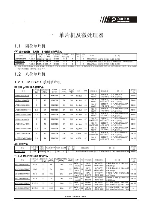
TI 公司 MSC121 混合信号产品
型号
工作电压 速度/频率 Flash RAM/EEPROM Timer
(V)
(MHz) (BYTE) (BYTE) /WDT
A/D I/O 串行通讯
MSC1210Y2PAGT 2.7-5
33
4K
常用的单片机品牌和型号介绍

常用的单片机品牌和型号介绍单片机(Microcontroller)是一种集成了微处理器核心、存储器和各种外设接口的集成电路,广泛应用于嵌入式系统中。
单片机能够完成各种控制和计算任务,因此在电子领域中使用非常广泛。
本文将介绍几个常用的单片机品牌和型号,以帮助读者选择适合自己项目的单片机。
一、STMicroelectronicsSTMicroelectronics(意法半导体)是全球领先的半导体供应商之一,提供多种单片机产品。
其中,STM32系列是STMicroelectronics最为著名的单片机系列之一,基于ARM Cortex-M内核。
STM32系列广泛应用于各种嵌入式设备,具有高性能、低功耗等特点。
常见的型号包括STM32F0、STM32F1、STM32F4等,适用于不同的应用场景。
二、AtmelAtmel是一家美国公司,也是全球最大的单片机供应商之一。
Atmel的AVR系列单片机以其高性能和易用性而闻名。
AVR系列单片机具有低功耗、快速执行速度和丰富的外设接口,非常适合于各种嵌入式应用。
其中,ATmega328P是最常用的型号之一,广泛使用于Arduino开发板等项目中。
三、Texas InstrumentsTexas Instruments(德州仪器)是一家世界领先的半导体公司,提供多种单片机产品。
MSP430系列是Texas Instruments的一系列低功耗、高集成度的单片机产品,适用于各种便携式设备和电池供电系统。
MSP430系列单片机具有强大的外设功能和丰富的存储器选项,常见的型号有MSP430G2553、MSP430F5529等。
四、MicrochipMicrochip是一家专注于微控制器和模拟半导体的供应商,其PIC 单片机系列非常知名。
PIC系列单片机具有低功耗、高稳定性和广泛的外设接口,适用于各种应用场景。
其中,PIC16F877A是最常用的型号之一,常见于工业自动化、家电控制等领域。
Atmel微控制器产品参考指南说明书

AVR for LCD Control
ATmega169P ATmega329P ATmega329 ATmega3290P ATmega3290 ATmega649 ATmega6490
Application Oriented
AVR for USB Connectivity
Flash Programming
Flexible Programming Implementation
Self-Program using any physical link!
In-System Programming
Parallel JTAG
The programming channels can be disabled to avoid any further download !
Product Range
Atmel microcontrollers - success through innovation
Product Range
&
quick reference guide
Product Range
Product Range
Product Families
tinyAVR® megaAVR® XMEGA™
AVR for Remote Access Control
AVR MCUs Are Designed to Program Themselves at Your Command
Flash Programming
&
quick reference guide
Self-Programming Flash – Key Benefits
英飞凌单片机选型手册
XC166 40 MHz, Single Cycle
XC164CS Mid-range
XC164CM Low-end
XC167 High-end Motor Ctrl
XC161 High-end
C500 20 MHz, 12 Cycle
C505 44 Pin, CAN
C515 80 Pin, CAN
with 2 Nodes
–
MultiCAN with 2 Nodes
✓
✓
3 + 1-ch
✓
2
✓
✓
✓
PG-TQFP-64
✓
–
✓
✓
3 + 1-ch
✓
2
✓
✓
✓
PG-TQFP-64
✓
MultiCAN with 2 Nodes
✓
✓
3 + 1-ch
✓
2
✓
✓
✓
PG-TQFP-64
32-bit Microcontrollers
8
8-bit Microcontrollers
C505CA
10
C515C
12
C868
14
XC866
16
XC886/888CLM
18
XC886/888LM
20
Starter Kits for 8-bit Microcontrollers
22
16-bit Microcontrollers
C161K/O
24
✓
2
✓
✓
✓
PG-TQFP-48
✓
–
✓
✓
3 + 1-ch
- 1、下载文档前请自行甄别文档内容的完整性,平台不提供额外的编辑、内容补充、找答案等附加服务。
- 2、"仅部分预览"的文档,不可在线预览部分如存在完整性等问题,可反馈申请退款(可完整预览的文档不适用该条件!)。
- 3、如文档侵犯您的权益,请联系客服反馈,我们会尽快为您处理(人工客服工作时间:9:00-18:30)。
Flash ISP (In-System Programmable)
芯片型号
描述
AT89C5115
Low-pin-count 8-bit Microcontroller with A/D Converter and 16K Bytes of Flash Memory We recommend to implement an external brown out to prevent any Flash/EEPROM corruption during power-on or power-off. Please refer to related application note: External Brown-out Protection for C51 Microcontrollers with Active High Reset Input
High performance 8-bit Microcontroller 16 kbytes Flash We recommend to implement an external brown out to prevent any Flash/EEPROM corruption during power-on or power-off. Please refer to related application note: External Brown-out Protection for C51 Microcontrollers with Active High Reset Input High performance 8-bit microcontroller 32 Kbytes Flash We recommend to implement an external brown out to prevent any Flash/EEPROM corruption during power-on or power-off. Please refer to related application note: External Brown-out Protection for C51 Microcontrollers with Active High Reset Input High performance 8-bit microcontroller with 64 Kbytes Flash
High performance 8-bit microcontroller with 128 Kbytes Flash Low-Voltage Microcontroller with 4K Bytes In-System Programmable Flash Low-Voltage Microcontroller with 8K Bytes In-System Programmable Flash 2.7-Volt 80C31 Microcontroller with 2K Bytes In-System Programmable Flash 20-pin Package. 2.7-Volt 80C31 Microcontroller with 4K Bytes In-System Programmable Flash 20-pin Package. 8-bit Microcontroller with 4K Bytes In-System Programmable Flash
AT89C51AC2
8-bit microcontroller with 32Kbyte Flash, 2KByte EEPROM and 10-bit A/D converter We recommend to implement an external brown out to prevent any Flash/EEPROM corruption during power-on or power-off. Please refer to related application note: External Brown-out Protection for C51 Microcontrollers with Active High Reset Input
AT89C51IC2 is a 80C51 8-bit microcontrollers featuring a 32K bytes Flash code memory and a two-wire interface (TWI).
High performance 8-bit microcontroller 64 Kbytes Flash, 2 Kbytes EEPROM and Two Wire Interface (TWI).
8-bit Microcontroller with 8K Bytes In-System Programmable Flash
AT89S8253
In-System Programmable Microcontroller with 12K bytes Flash 2K bytes EEPROM
Flash ISP - Single Cycle Core 芯片型号
● 4 KB version: AT89LP4052
AT89LP4052
4-Kbyte In-system Flash -- Single-Cycle Microcontroller 256 Bytes RAM,SPI PWM,20 MIPS Throughput at 20 MHz.. ● 2 KB version: AT89LP2052
8051结构单片机选型参数表
● OTP (One-Time Programmable) ● ROM ● ROMless ● USB MCUs
芯片型号 AT89C51CC03
CAN Networking MCUs
描述 8-bit microcontroller with CAN controller and 64-Kbyte Flash. 2-Kbyte RAM, 2-Kbyte EEPROM, SPI. Power Fail Detect (no need for external brown- out). Pinout compatible with T89C51CC01.
8-bit microcontroller with CAN controller and 32- Kbyte Flash AT89C51CC01 T89C51CC01 We recommend to implement an external brown out to prevent any Flash/EEPROM corruption during power-on or power-off. Please refer to
AT89C51ED2 AT89C51IC2 AT89C51ID2
AT89C51RB2
AT89Байду номын сангаас51RC2
AT89C51RD2 AT89C51RE2 AT89LS51 AT89LS52 AT89S2051 AT89S4051 AT89S51 AT89S52
High performance 8-bit microcontroller 64 Kbytes Flash, 2 Kbytes EEPROM
AT89LP214 AT89LP216
AT89LP2052
2-Kbyte In-system Programmable Flash -- Single Cycle 8051 Microcontroller 128 Bytes RAM UART SPI I/O = 12 Analog Comparator Internal RC Oscillator On-chip Debug 2-Kbyte In-system Programmable Flash -- Single Cycle 8051 Microcontroller 128 Bytes RAM PWM UART SPI I/O = 16,Analog Comparator, Internal RC Oscillator,On-chip Debug 2-Kbyte In-system Flash -- Single-Cycle Microcontroller,256 Bytes RAM,SPI,PWM,20 MIPS Throughput at 20 MHz..
AT89LP213
描述
2-Kbyte In-system Programmable Flash -- Single Cycle 8051 Microcontroller, 128 Bytes RAM, PWM, SPI, I/O = 12, Analog Comparator, Internal RC Oscillator, On-chip Debug
● CAN Networking MCUs ● Flash (Reprogrammable) ● Flash ISP (In-System Programmable) ● Flash ISP - Single Cycle Core ● Lighting MCUs
ATMEL 爱特梅尔 > 8051结构单片机
Lighting MCUs 芯片型号 AT83EB5114 AT89EB5114
描述
Dedicated to lighting control applications,the AT83EB5114 retains all the features of the standard 80C51 with 4 Kbytes ROM program memory,256 bytes RAM,256 bytes EEPROM,a 7-source,4-level interrupt system,an onchip oscillator and two timers/counters. Analog functions include a 10-bit,6 channels A/D converter and two optimized PWM units.