testbench时钟信号的编写(verilog)
verilogtestbench写法

verilogtestbench写法Verilog测试平台(testbench)技术(⼀) 收藏对设计进⾏功能仿真和时序仿真时,需要给待测模块提供激励输⼊。
对于由Verilog语⾔描述的设计模块,最好的⽅法⾃然同样是⽤Verilog语⾔对待测模块施加激励和检测模块的输出响应。
实际应⽤中,Verilog测试平台(testben ch)就是⽤来提供上述功能的。
Verilog测试平台是⼀个例化的待测(MUT)Verilog 模块,给它施加激励并观测其输出。
由于测试平台是⽤Verilog语⾔描述的,因此可以应⽤到不同的仿真环境中。
待测模块和与之对应的测试平台组成⼀个仿真模型,应⽤这个模型可以在不同的测试环境中⽤相同的激励对待测模块进⾏调试。
下⾯就对不同电路类型分别介绍verilog测试平台的语⾔结构。
⼀、测试平台1.组合电路测试设计组合电路的测试平台时,待测模块及其功能决定了激烈的选择与测试次数。
对于⼀个已有的待测模块,测试平台中需要声明与待测模块输⼊输出端⼝对应的变量。
与输⼊端⼝相连接的变量定义为reg,与输出端⼝相连接的变量定义为wire,例化时将测试平台中声明的变量与待测模块的输⼊输出端⼝相关联。
使⽤initial语句控制程序运⾏,initial语句是⼀种过程结构,在initial块中可使⽤延迟控制语句来控制initial块中的程序流动。
这⾥对⼀个简单的算术逻辑单元(ALU)为例进⾏测试,下⾯是该单元Verilog 描述。
/***************************************************************** ********///多动能ALU的Verilog代码'timescale 1ns/100psmodule alu_4bit(a,b,f,oe,y,p,ov,a_gt_b,a_eg_b,a_lt_b);input [3:0] a,b;input [1:0] f;input oe;input [3:0] y;output p,ov,a_gt_b,a_eg_b,a_lt_b; reg [4:0] im_y;always @(a or b or f)beginov=1'b0;im_y=0;case(f)2'b00:beginim_y=a+b;if(im_y>5'b01111)ov=1'b1;end2'b01:beginim_y=a-b;if(im_y>5'b01111)ov=1'b1;end2'b10:im_y[3:0]=a&b;2'b11:im_y[3:0]=a^b;default:im_y[3:0]=4'b0000;endcaseendalways @(a or b)beginif(a>b){a_gt_b,a_ge_b,a_lt_b}=3'b100;else if(a{a_gt_b,a_ge_b,a_lt_b}=3'b001;else{a_gt_b,a_ge_b,a_lt_b}=3'b010;endassign p=^im_y[3:0];assign y=oe?im_y[3:0]:4'bz;endmodule/***************************************************************** ********/模块alu_4bit是四功能的算术逻辑单元,输⼊包括数据信号a、b和功能信号f,输出包括数据信号y和ALU⽣成的奇偶校验信号p、溢出信号ov及⽐较信号。
编写高效率的testbench
编写高效率的testbench简介:由于设计的规模越来越大也越来越复杂,数字设计的验证已经成为一个日益困难和繁琐的任务。
验证工程师们依靠一些验证工具和方法来应付这个挑战。
对于几百万门的大型设计,工程师们一般使用一套形式验证(formal verification)工具。
然而对于一些小型的设计,设计工程师常常发现用带有testbench的HDL仿真器就可以很好地进行验证。
Testbench已经成为一个验证高级语言(HLL --High-Level Language) 设计的标准方法。
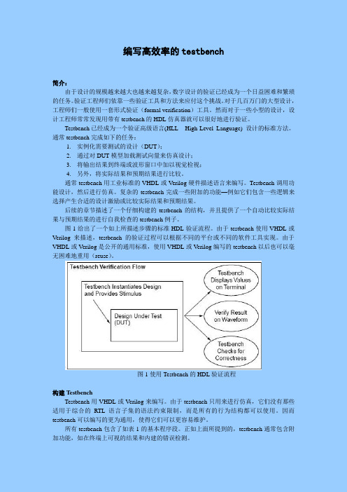
通常testbench完成如下的任务:1.实例化需要测试的设计(DUT);2.通过对DUT模型加载测试向量来仿真设计;3.将输出结果到终端或波形窗口中加以视觉检视;4.另外,将实际结果和预期结果进行比较。
通常testbench用工业标准的VHDL或Verilog硬件描述语言来编写。
Testbench调用功能设计,然后进行仿真。
复杂的testbench完成一些附加的功能—例如它们包含一些逻辑来选择产生合适的设计激励或比较实际结果和预期结果。
后续的章节描述了一个仔细构建的testbench的结构,并且提供了一个自动比较实际结果与预期结果的进行自我检查的testbench例子。
图1给出了一个如上所描述步骤的标准HDL验证流程。
由于testbench使用VHDL或Verilog来描述,testbench的验证过程可以根据不同的平台或不同的软件工具实现。
由于VHDL或Verilog是公开的通用标准,使用VHDL或Verilog编写的testbench以后也可以毫无困难地重用(reuse)。
图1使用Testbench的HDL验证流程构建TestbenchTestbench用VHDL或Verilog来编写。
由于testbench只用来进行仿真,它们没有那些适用于综合的RTL语言子集的语法约束限制,而是所有的行为结构都可以使用。
因而testbench可以编写的更为通用,使得它们可以更容易维护。
VHDL——如何写简单的testbench
use ieee.std_logic_1164.all;use ieee.std_logic_arith.all;--use ieee.std_logic_unsigned.all;entity cnt6 isport(clr,en,clk :in std_logic;q :out std_logic_vector(2 downto 0) );end entity;architecture rtl of cnt6 issignal tmp :std_logic_vector(2 downto 0); beginprocess(clk)-- variable q6:integer;beginif(clk'event and clk='1') thenif(clr='0')thentmp<="000";elsif(en='1') thenif(tmp="101")thentmp<="000";elsetmp<=unsigned(tmp)+'1';end if;end if;end if;q<=tmp;-- qa<=q(0);-- qb<=q(1);-- qc<=q(2);end process;end rtl;二、六进制计数器testbench的代码signal en :std_logic:='0';signal clk :std_logic:='0';signal q :std_logic_vector(2 downto 0);constant clk_period :time :=20 ns;begininstant:cnt6 port map(clk=>clk,en=>en,clr=>clr,q=>q);clk_gen:processbeginwait for clk_period/2;clk<='1';wait for clk_period/2;clk<='0';end process;clr_gen:processbeginclr<='0';wait for 30 ns;clr<='1';wait;end process;en_gen:processbeginen<='0';wait for 50ns;en<='1';wait;end process;end rtl;--测试平台文件(testbench)的基本结构library ieee;use ieee.std_logic_1164.all;entity test_bench is --测试平台文件的空实体(不需要端口定义) end test_bench;architecture tb_behavior of test_bench iscomponent entity_under_test --被测试元件的声明port(list-of-ports-theri-types-and-modes);end component;begininstantiation:entity_under_test port map(port-associations);process() --产生时钟信号……end process;process() --产生激励源……end process;end tb_behavior;------------------------------------------------------------------- --简单计数程序源码library ieee;use ieee.std_logic_1164.all;use ieee.std_logic_unsigned.all;use ieee.std_logic_unsigned.all;entity sim_counter isport(clk :in std_logic;reset :in std_logic;count :out std_logic_vector(3 downto 0));end entity;architecture behavioral of sim_counter issignal temp :std_logic_vector(3 downto 0);beginprocess(clk,reset)beginif reset='1' thentemp<="0000";elsif clk'event and clk='1' thentemp<=temp+1;end if;end process;count<=temp;end behavioral;------------------------------------------------------------------- --简单计数程序,测试文件代码(testbench)library ieee;use ieee.std_logic_1164.all;use ieee.std_logic_unsigned.all;use ieee.numeric_std.all;entity counter_tb_vhd is --测试平台实体end counter_tb_vhd;architecture behavior of counter_tb_vhd is--被测试元件(DUT)的声明component sim_counterport(clk :in std_logic;reset :in std_logic;count :out std_logic_vector(3 downto 0));end component;--输入信号signal clk:std_logic:='0';signal reset :std_logic:='0';--输出信号signal count :std_logic_vector(3 downto 0);constant clk_period :time :=20 ns; --时钟周期的定义begindut:sim_counter port map(clk=>clk,reset=>reset,counter=>counter);clk_gen:processbeginclk='1';wait for clk_period/2;clk='0';wait for clk_period/2;end process;tb:process --激励信号beginwait for 20 ns;reset<='1';wait for 20 ns;reset<='0';wait for 200 ns;wait; --will wait forever;end process;end;--激励信号的产生方式--1.以一定的离散时间间隔产生激励信号的波形--2.基于实体的状态产生激励信号,也就是说基于实体的输出响应产生激励信号--两种常用的复位信号--1.周期性的激励信号,如时钟--2.时序变化的激励型号,如复位--eg.产生不对称时钟信号w_clk<='0' after period/4 when w_clk='1' else'1' after 3*period/4 when w_clk='0' else'0';--eg.产生堆成时钟信号,process语句clk_gen1:processconstan clk_period := 40 ns;beginclk='1';wait for clk_period/2;clk='0';wait for clk_period/2;end process;四、如果自己不想写这些testbench的这些固定格式,可以在quartus 里自动生成testbench文件的模板,然后往里面写信号就行了步骤:processing->start->start test bench template write这里需要注意的是要在仿真选项里选择一个仿真工具,然后才会生成testbench自动生成的testbench模板格式如下:-- Copyright (C) 1991-2008 Altera Corporation-- Your use of Altera Corporation's design tools, logic functions-- and other software and tools, and its AMPP partner logic-- functions, and any output files from any of the foregoing-- (including device programming or simulation files), and any-- associated documentation or information are expressly subject-- to the terms and conditions of the Altera Program License-- Subscription Agreement, Altera MegaCore Function License-- Agreement, or other applicable license agreement, including,-- without limitation, that your use is for the sole purpose of-- programming logic devices manufactured by Altera and sold by-- Altera or its authorized distributors. Please refer to the-- applicable agreement for further details.-- ***************************************************************************-- This file contains a Vhdl test bench template that is freely editable to-- suit user's needs .Comments are provided in each section to help the user -- fill out necessary details.-- ***************************************************************************-- Generated on "03/13/2011 20:05:04"-- Vhdl Test Bench template for design : cnt6---- Simulation tool : ModelSim (VHDL)--LIBRARY ieee;USE ieee.std_logic_1164.all;ENTITY cnt6_vhd_tst ISEND cnt6_vhd_tst;ARCHITECTURE cnt6_arch OF cnt6_vhd_tst IS-- constants-- signalsSIGNAL clk : STD_LOGIC;SIGNAL clr : STD_LOGIC;SIGNAL en : STD_LOGIC;SIGNAL q : STD_LOGIC_VECTOR(2 DOWNTO 0);COMPONENT cnt6PORT (clk : IN STD_LOGIC;clr : IN STD_LOGIC;en : IN STD_LOGIC;q : OUT STD_LOGIC_VECTOR(2 DOWNTO 0));END COMPONENT;BEGINi1 : cnt6PORT MAP (-- list connections between master ports and signalsclk => clk,clr => clr,en => en,q => q);init : PROCESS-- variable declarationsBEGIN-- code that executes only onceWAIT;END PROCESS init;always : PROCESS-- optional sensitivity list-- ( )-- variable declarationsBEGIN-- code executes for every event on sensitivity list WAIT;END PROCESS always;END cnt6_arch;。
组合-时序逻辑电路Verilog-Testbench代码_带仿真代码和波形_

1组合逻辑电路--基本门电路1.1基本门电路1.1.1结构化描述方式代码如下View Code1 module logics2 (3 input iA,4 input iB,5 output oAnd,6 output oOr,7 output oNot8 );910 and and_inst(oAnd,iA,iB);11 or or_inst(oOr,iA,iB);12 not not_inst(oNot,iA);1314 endmodule最底层的是门级原语and or not RTL级视图testbench如下View Code1 `timescale 1 ns/ 1 ns2 module logics_tb();34 reg ia;5 reg ib;67 wire oAnd;8 wire oOr;9 wire oNot;1011 initial12 begin13 ia=0;14 #40 ia=1;15 #40 ia=0;16 #40 ia=1;17 #40 ia=0;18 end1920 initial21 begin22 ib=0;23 #40 ib=0;24 #40 ib=1;25 #40 ib=1;26 #40 ib=0;27 end2829 logics logics_inst30 (31 .iA(ia),32 .iB(ib),33 .oAnd(oAnd),34 .oOr(oOr),35 .oNot(oNot)36 );3738 endmoduleRTL级仿真图形如下GATE级仿真图如下可见RTL级仿真是理想的,GATE级仿真考虑了延迟和信号开始的不确定。
1.1.2采用流描述方法代码如下View Code1 module logics2 (3 input iA,4 input iB,5 output oAnd,6 output oOr,7 output oNot8 );910 assign oAnd=iA&iB;11 assign oOr=iA|iB;12 assign oNot=~iA;1314 endmoduleRTL级视图,仿真图形同上。
verilog testbench语法
verilog testbench语法Verilog testbench 是用来对 Verilog 设计进行仿真验证的代码。
它提供了一系列的输入信号和时钟,以及对输出结果的预期值进行比较,以验证设计的正确性。
以下是 Verilog testbench 的基本语法:1. 模块定义:```module testbench_name;// 输入输出信号声明// 实例化需要测试的模块// 给输入信号赋值// 检查输出信号和预期结果是否相符endmodule```2. 时钟定义:```reg clk; // 定义时钟信号always #5 clk = ~clk; // 定义时钟周期```3. 输入信号声明和赋值:```reg input1;wire expected_output;reg [3:0] array_input [7:0];// 给输入信号赋值initial begininput1 = 1'b0;#10;input1 = 1'b1;#10;//...end```4. 实例化需要测试的模块:```// 通过实例化需要测试的模块// 给模块的输入端口连接输入信号// 给模块的输出端口连接输出信号// 在 testbench 中实例化被测试的模块//...```5. 检查输出信号和预期结果:```// 在仿真过程中,通过比较输出信号和预期结果来验证设计的正确性// 根据需要使用相应的比较语句,如 `==`, `!=`, `===`, `!==`, `>`, `<` 等// 在每个时钟周期末检查预期输出结果//...```这些是 Verilog testbench 的基本语法。
在具体的测试中,需要根据设计的功能和需求来给输入信号赋值,并检查输出信号和预期结果是否一致。
Verilog-testbench的写法

数字集成电路设计入门--从HDL到版图于敦山北大微电子学系第十五章Verilog Test Bench使用简介学习内容:•用一个复杂的test bench复习设计的组织与仿真•建立test bench通常使用的编码风格及方法设计组织虚线表示编译时检测输入文件是否存在及可读并允许生成输出文件。
test bench 组织stimulus要验证的设计简单的test bench•简单的test bench 向要验证的设计提供向量,人工验证输出。
•复杂的test bench 是自检测的,其结果自动验证。
复杂的test bench激励验证结果要验证的设计并行块•fork…join块在测试文件中很常用。
他们的并行特性使用户可以说明绝对时间,并且可以并行的执行复杂的过程结构,如循环或任务。
module inline_ tb;reg [7: 0] data_ bus;// instance of DUTinitial forkdata_bus = 8'b00;Time | data_ bus0 | 8’b0000_0000 10 | 8’b0100_0101 30 | 8’b0100_0110 40 | 8’b0100_0111 45 | 8’b1000_1110#10 data_bus = 8'h45;#20 repeat (10) #10 data_bus = data_bus + 1;#25 repeat (5) #20 data_bus = data_bus<< 1;#140 data_bus = 8'h0f;joinendmodule上面的两个repeat循环从不同时间开始,并行执行。
象这样的特殊的激励集在单个的begin…end块中将很难实现。
50 | 8’b1000_1111 60 | 8’b1001_0000 65 | 8’b0010_0000 70 | 8’b0010_0001 80 | 8’b0010_0010 85 | 8’b0100_0100 90 | 8’b0100_0101 100 | 8’b0100_0110 105 | 8’b1000_1100 110 | 8’b1000_1101 120 | 8’b1000_1110 125 | 8’b0001_1100 140 | 8’b0000_1111包含文件•包含文件用于读入代码的重复部分或公共数据。
如何编写testbench的总结(非常实用的总结)
如何编写testbench的总结(⾮常实⽤的总结)1.激励的设置相应于被测试模块的输⼊激励设置为reg型,输出相应设置为wire类型,双向端⼝inout在测试中需要进⾏处理。
⽅法1:为双向端⼝设置中间变量inout_reg作为该inout的输出寄存,inout⼝在testbench中要定义为wire型变量,然后⽤输出使能控制传输⽅向。
eg:inout [0:0] bi_dir_port;wire [0:0] bi_dir_port;reg [0:0] bi_dir_port_reg;reg bi_dir_port_oe;assign bi_dir_port=bi_dir_port_oe?bi_dir_port_reg:1'bz;⽤bi_dir_port_oe控制端⼝数据⽅向,并利⽤中间变量寄存器改变其值。
等于两个模块之间⽤inout双向⼝互连。
往端⼝写(就是往模块⾥⾯输⼊)⽅法2:使⽤force和release语句,这种⽅法不能准确反映双向端⼝的信号变化,但这种⽅法可以反映块内信号的变化。
具体如⽰:module test();wire data_inout;reg data_reg;reg link;#xx; //延时force data_inout=1'bx; //强制作为输⼊端⼝...............#xx;release data_inout; //释放输⼊端⼝endmodule从⽂本⽂件中读取和写⼊向量1)读取⽂本⽂件:⽤ $readmemb系统任务从⽂本⽂件中读取⼆进制向量(可以包含输⼊激励和输出期望值)。
$readmemh ⽤于读取⼗六进制⽂件。
例如:reg [7:0] mem[1:256] // a 8-bit, 256-word 定义存储器meminitial $readmemh ( "mem.data", mem ) // 将.dat⽂件读⼊寄存器mem中initial $readmemh ( "mem.data", mem, 128, 1 ) // 参数为寄存器加载数据的地址始终2)输出⽂本⽂件:打开输出⽂件⽤?$fopen 例如:integer out_file; // out_file 是⼀个⽂件描述,需要定义为 integer类型out_file = $fopen ( " cpu.data " ); // cpu.data 是需要打开的⽂件,也就是最终的输出⽂本设计中的信号值可以通过$fmonitor, $fdisplay,2. Verilog和Ncverilog命令使⽤库⽂件或库⽬录ex). ncverilog -f run.f -v lib/lib.v -y lib2 +libext+.v //⼀般编译⽂件在run.f中, 库⽂件在lib.v中,lib2⽬录中的.v⽂件系统⾃动搜索使⽤库⽂件或库⽬录,只编译需要的模块⽽不必全部编译3.Verilog Testbench信号记录的系统任务:1). SHM数据库可以记录在设计仿真过程中信号的变化. 它只在probes有效的时间内记录你set probe on的信号的变化.ex). $shm_open("waves.shm"); //打开波形数据库$shm_probe(top, "AS"); // set probe on "top",第⼆个参数: A -- signals of the specific scropeS -- Ports of the specified scope and below, excluding library cellsC -- Ports of the specified scope and below, including library cellsAS -- Signals of the specified scope and below, excluding library cellsAC -- Signals of the specified scope and below, including library cells还有⼀个 M ,表⽰当前scope的memories, 可以跟上⾯的结合使⽤, "AM" "AMS" "AMC"什么都不加表⽰当前scope的ports;$shm_close //关闭数据库2). VCD数据库也可以记录在设计仿真过程中信号的变化. 它只记录你选择的信号的变化.ex). $dumpfile("filename"); //打开数据库$dumpvars(1, top.u1); //scope = top.u1, depth = 1第⼀个参数表⽰深度, 为0时记录所有深度; 第⼆个参数表⽰scope,省略时表当前的scope.$dumpvars; //depth = all scope = all$dumpvars(0); //depth = all scope = current$dumpvars(1, top.u1); //depth = 1 scope = top.u1$dumpoff //暂停记录数据改变,信号变化不写⼊库⽂件中$dumpon //重新恢复记录3). Debussy fsdb数据库也可以记录信号的变化,它的优势是可以跟debussy结合,⽅便调试.如果要在ncverilog仿真时,记录信号, ⾸先要设置debussy:a. setenv LD_LIBRARY_PATH :$LD_LIBRARY_PATH(path for debpli.so file (/share/PLI/nc_xl//nc_loadpli1))b. while invoking ncverilog use the +ncloadpli1 option.ncverilog -f run.f +debug +ncloadpli1=debpli:deb_PLIPtrfsdb数据库⽂件的记录⽅法,是使⽤$fsdbDumpfile和$fsdbDumpvars系统函数,使⽤⽅法参见VCD注意: 在⽤ncverilog的时候,为了正确地记录波形,要使⽤参数: "+access+rw", 否则没有读写权限在记录信号或者波形时需要指出被记录信号的路径,如:tb.module.u1.clk.………………………………………………………………………………………………………关于信号记录的系统任务的说明:在testbench中使⽤信号记录的系统任务,就可以将⾃⼰需要的部分的结果以及波形⽂件记录下来(可采⽤sigalscan⼯具查看),适⽤于对较⼤的系统进⾏仿真,速度快,优于全局仿真。
verilog时钟分频设计
verilog时钟分频设计1.偶分频模块设计偶分频意思是时钟模块设计最为简单。
首先得到分频系数M和计数器值N。
M = 时钟输入频率 / 时钟输出频率N = M / 2如输入时钟为50M,输出时钟为25M,则M=2,N=1。
偶分频则意味着M为偶数。
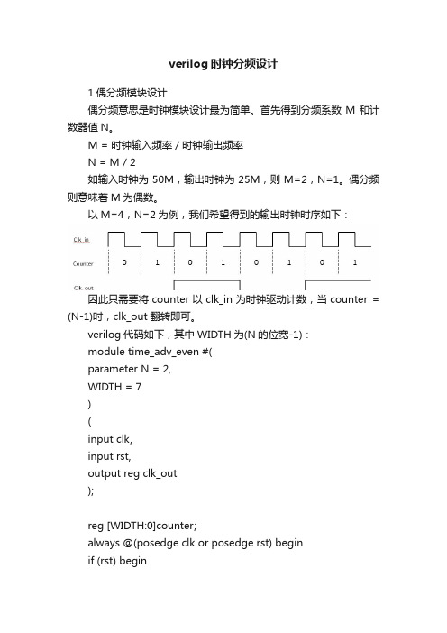
以M=4,N=2为例,我们希望得到的输出时钟时序如下:因此只需要将counter以clk_in为时钟驱动计数,当counter = (N-1)时,clk_out翻转即可。
verilog代码如下,其中WIDTH为(N的位宽-1):module time_adv_even #(parameter N = 2,WIDTH = 7)(input clk,input rst,output reg clk_out);reg [WIDTH:0]counter;always @(posedge clk or posedge rst) beginif (rst) begin// resetcounter <= 0;endelse if (counter == N-1) begincounter <= 0;endelse begincounter <= counter + 1;endendalways @(posedge clk or posedge rst) beginif (rst) begin// resetclk_out <= 0;endelse if (counter == N-1) beginclk_out <= !clk_out;endendendmoduletestbench测试8分频即N=4,ISE仿真结果如下:2.奇分频模块设计奇分频需要通过两个时钟共同得到。
首先得到分频系数M和计数器值N。
M = 时钟输入频率 / 时钟输出频率N = (M-1) / 2如输入时钟为50M,输出时钟为10M,则M=5,N=2。
奇分频则意味着M为奇数。