DS18B20温度传感器英文介绍
单总线温度传感器DS18B20简介

单总线温度传感器DS18B20简介DS18B20是DALLAS公司生产的单总线式数字温度传感器,它具有微型化、低功耗、高性能、搞干扰能力强、易配处理器等优点,特别适用于构成多点温度测控系统,可直接将温度转化成串行数字信号(提供9位二进制数字)给单片机处理,且在同一总线上可以挂接多个传感器芯片。
它具有3引脚TO-92小体积封装形式,温度测量范围为-55℃~+125℃,可编程为9位~12位A/D转换精度,测温分辨率可达0.0625℃,被测温度用符号扩展的16位数字量方式串行输出,其工作电源既可在远端引入,也可采用寄生电源方式产生,多个DS18B20可以并联到3根或2根线上,CPU只需一根端口线就能与多个DS18B20通信,占用微处理器的端口较少,可节省大量的引线和逻辑电路。
以上特点使DS18B20非常适用于远距离多点温度检测系统。
DS18B20外形及引脚说明外形及引脚如图2所示:图2 管脚排列图在TO-92和SO-8的封装中引脚有所不同,具体差别请查阅PDF手册,在TO-92封装中引脚分配如下:1(GND):地2(DQ):单线运用的数据输入输出引脚3(VDD):可选的电源引脚DS18B20工作过程及时序DS18B20内部的低温度系数振荡器是一个振荡频率随温度变化很小的振荡器,为计数器1提供一频率稳定的计数脉冲。
高温度系数振荡器是一个振荡频率对温度很敏感的振荡器,为计数器2提供一个频率随温度变化的计数脉冲。
初始时,温度寄存器被预置成-55℃,每当计数器1从预置数开始减计数到0时,温度寄存器中寄存的温度值就增加1℃,这个过程重复进行,直到计数器2计数到0时便停止。
初始时,计数器1预置的是与-55℃相对应的一个预置值。
以后计数器1每一个循环的预置数都由斜率累加器提供。
为了补偿振荡器温度特性的非线性性,斜率累加器提供的预置数也随温度相应变化。
计数器1的预置数也就是在给定温度处使温度寄存器寄存值增加1℃计数器所需要的计数个数。
温度传感器DS18B20_外文翻译
DS18B20Programmable Resolution1-WireDigital Thermometer1、DS18B20FEATURES(1)Unique1-Wire interface requires only one Port pin for communication,requires no external components(2)Each device has a unique64-bit serial code stored in an onboard ROM(3)Can be powered form data line.Power supply range is3.0Vto5.5V(4)Measures temperatures form-55℃to+125℃,±0.5℃accuracy from-10℃to +85℃(5)Thermometer resolution is user-selected from9to12bits(6)Converts temperature to12-bit digital word in750ms(max)(7)Alarm search command identifies and addresses devices whose temperature is outside of programmed limits(temperature alarm condition)(8)Available in8-pin SOIC,and3-bin TO-92packages2、DS18B20BLOCK DIAFRAMFigure1shows a block diagram of the DS18B20,The64-bite ROM stores the device’s serial code.The scratchpad memory contains the2-byte temperature egister that stores the digital output from the temperature sensor.In addition,the scratchpad provides access to the1-byte upper and lower alarm trigger register(TH and TL),and the1-byte configuratuion register.The configuration register allows the user to set the resolution of the temperature-to-digital conversion to9,10,11or12bits.The TH,TL and configuration registers are nonvolatile(EEPROM),so they will retain data when the device is powered down.Figure1block diagram of the DS18B203、DS18B20ROM COMMANDS(1)SEARCH ROM[0F0H]When a system is initially powered up,the master must identify the ROM codes of all slave devices on the bus,which allows the master to determine the number of slaves and their device types.The master learns the ROM codes through a process of elimination that requires the master to perform a Search ROM cycle as many times as necessary to identify all of the slave’s64-bit ROM devices.(2)READ ROM[55H]This command can only be used when there is one slave on the bus.It allows the bus master to read the slave`64-bit ROM code without using the Search ROM procedure.If this command is used when there is more than one slave present on the bus,a data collision will occur when all the slaves attempt to respond at the same time.(3)MATCH ROM[55H]The match ROM command followed by a64-bit ROM code sequence allows the bus master to address a specific DS18B20on a multidrop or single-drop bus.Only the DS18B20that exactly matches the64-bitROM code sequence will respond to thefunction command issued by the master;all other slaves on the bus will wait for a reset pulse.(4)SKIP ROM[0CCH]The master can use this command to address all devices on the bus simultaneously without sending out any ROM code information.Note that the Read Scratchpad command can follow the Skip ROM command only if there is a single slave device on the bus.In this case time is saved by allowing the master to read from the slave without sending the device’s64-bit ROM code.A Skip ROM command followed by a Read Scratchpad command will cause a data collision on the bus if there is more than one slave since multiple devices will attempt to transmit data simultaneously.(5)ALARM SEARCH[0ECH]The operation of this command is identical to the operation of the Search ROM command except that only slaves with a set alarm flag will respond.This command allows the master device to determine if any DS18B20s experienced an alarm condition during the most recent temperature conversion.Refer to the OPERATION-ALARM SIGNAING section for an explanation of alarm flag operation.(6)CONVERTT[44H]This command initiates a single temperature conversion.Following the conversion,the resulting thermal data is stored in the2-bute temperature register in the scratchpad memory and the DS18B20returns to its low-power idle state.If the device is being used in parasite power mode,within10us after this command is issued the master must enable a strong pullup on the1-Wire bus for the duration of the conversion as described in the POWERING THE DS18320section.If the DS18B20 is powered by an external supply,the master can issue read time slots after the Convert T command and the DS18B20will respond by transmitting a0while the temperature conversion is in Progress and a1when the conversion is done.In parasite power mode this notification technique cannot be used since the bus1is pulled high by the strong pullup during the conversion.(7)WRITE SCRACHPAD[4EH]This command allows the master to write3bytes of the data to the DS18B20’s scratchpad.The first data byte is writer into the TH register,the second byte is written into the TL register,and the third byte is written into the configuration register. Data must be transmitted least significant bit first.All three bytes must be written before the master issues a reset,or the data may be corrupted.(8)READ SCRACHPAD[0BEH]This command allows the master to read the contents of the scratchpad.The data transfer starts with the least significant bit of byte0and continues through the scratchpad until9byte(byte8-CRC)is read.The master may issue a reset to terminate reading at any time if only partof the scratchpad data is needed.(9)COPY SCRATCHPAD[48H]This command copies the contents of the scratchpad TH,TL and configuration registers to EEPROM.If the device is being used in parasite power mode,within 10us(max)after this command is issued the master must enable a strong pullup on the 1-Wire bus for at least10ms as described in the POWERING THE DS18B20section.(10)RECALL E2[B8H]This command recalls the alarm trigger values(TH and TL)and configuration data from EEPROM,respectively,in the scratchpad memory.The master device can issue read time slots following the Recall E2command and the DS18B20will indicate the status of the recall by transmitting0while the recall is in progress and1 when the recall is done.The recall operation happens automatically at power-up,so valid data is available in the scratchpad as soon as power is applied to the device.DS18B20单总线数字温度计1、DS18B20的特性(1)独特的单总线接口只占用一个I/O端口,而无需外围元件;(2)可以由总线提供电源,电压适用范围为3.0V~5.5V;(3)测量温度范围为-55℃~+125℃,在-10℃~+85℃范围内精度为±0.5℃;(4)每个DS18B20含有一个唯一的64位ROM编码;(5)用户可以通过编程实现9~12位的温度分辨率;(6)分辨率为12时最大转换时间为750ms;(7)报警搜索命令可识别哪片DS18B20温度超限;(8)采用3脚T0-92或8脚SOIC封装。
DS18B20是美国DALLAS半导体公司继DS1820之后最新推出的(精)
DS18B20是美国DALLAS半导体公司继DS1820之后最新推出的一种改进型智能温度传感器。
与传统的热敏电阻相比,他能够直接读出被测温度并且可根据实际要求通过简单的编程实现9~12位的数字值读数方式。
可以分别在93.75 ms和750 ms内完成9位和12位的数字量,并且从DS18B20读出的信息或写入DS18B2 0的信息仅需要一根口线(单线接口)读写,温度变换功率来源于数据总线,总线本身也可以向所挂接的DS1 8B20供电,而无需额外电源。
因而使用DS18B20可使系统结构更趋简单,可靠性更高。
他在测温精度、转换时间、传输距离、分辨率等方面较DS1820有了很大的改进,给用户带来了更方便的使用和更令人满意的效果。
1 DS18B20简介(1)独特的单线接口方式:DS18B20与微处理器连接时仅需要一条口线即可实现微处理器与DS18B20的双向通讯。
(2)在使用中不需要任何外围元件。
(3)可用数据线供电,电压范围:3.0" 5.5 V。
(4)测温范围:-55 " 125 ℃。
固有测温分辨率为0.5 ℃。
(5)通过编程可实现9"12位的数字读数方式。
(6)用户可自设定非易失性的报警上下限值。
(7)支持多点组网功能,多个DS18B20可以并联在惟一的三线上,实现多点测温。
(8)负压特性,电源极性接反时,温度计不会因发热而烧毁,但不能正常工作。
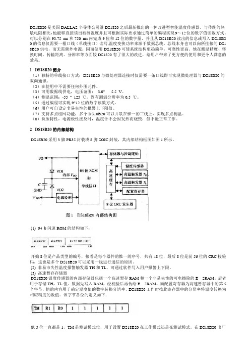
2 DS18B20的内部结构DS18B20采用3脚PR35封装或8脚SOIC封装,其内部结构框图如图1所示。
(1) 64 b闪速ROM的结构如下:开始8位是产品类型的编号,接着是每个器件的惟一的序号,共有48位,最后8位是前56位的CRC校验码,这也是多个DS18B20可以采用一线进行通信的原因。
(2) 非易市失性温度报警触发器TH和TL,可通过软件写入用户报警上下限。
(3) 高速暂存存储器DS18B20温度传感器的内部存储器包括一个高速暂存RAM和一个非易失性的可电擦除的E 2RAM。
DS18B20是美国DALLAS半导体公司继DS1820之后最新推出的(精)
DS18B20是美国DALLAS半导体公司继DS1820之后最新推出的一种改进型智能温度传感器。
与传统的热敏电阻相比,他能够直接读出被测温度并且可根据实际要求通过简单的编程实现9~12位的数字值读数方式。
可以分别在93.75 ms和750 ms内完成9位和12位的数字量,并且从DS18B20读出的信息或写入DS18B2 0的信息仅需要一根口线(单线接口)读写,温度变换功率来源于数据总线,总线本身也可以向所挂接的DS1 8B20供电,而无需额外电源。
因而使用DS18B20可使系统结构更趋简单,可靠性更高。
他在测温精度、转换时间、传输距离、分辨率等方面较DS1820有了很大的改进,给用户带来了更方便的使用和更令人满意的效果。
1 DS18B20简介(1)独特的单线接口方式:DS18B20与微处理器连接时仅需要一条口线即可实现微处理器与DS18B20的双向通讯。
(2)在使用中不需要任何外围元件。
(3)可用数据线供电,电压范围:3.0" 5.5 V。
(4)测温范围:-55 " 125 ℃。
固有测温分辨率为0.5 ℃。
(5)通过编程可实现9"12位的数字读数方式。
(6)用户可自设定非易失性的报警上下限值。
(7)支持多点组网功能,多个DS18B20可以并联在惟一的三线上,实现多点测温。
(8)负压特性,电源极性接反时,温度计不会因发热而烧毁,但不能正常工作。
2 DS18B20的内部结构DS18B20采用3脚PR35封装或8脚SOIC封装,其内部结构框图如图1所示。
(1) 64 b闪速ROM的结构如下:开始8位是产品类型的编号,接着是每个器件的惟一的序号,共有48位,最后8位是前56位的CRC校验码,这也是多个DS18B20可以采用一线进行通信的原因。
(2) 非易市失性温度报警触发器TH和TL,可通过软件写入用户报警上下限。
(3) 高速暂存存储器DS18B20温度传感器的内部存储器包括一个高速暂存RAM和一个非易失性的可电擦除的E 2RAM。
DS18B20资料中英文翻译
The DS-18B20 number temperature spreads a feeling machine The DS-18B20 number temperature spreads a feeling machine, the product adoption's United States' DALLAS company produces of DS18 B20 can set net number the temperature spread the feeling machine chip to pack but become and have to bear to whet to bear to touch, the physical volume is small, use convenience, seal to pack a form diverse, be applicable to various narrow and small space equipments number to measure moderate control realm.1、the technique function describe:1.1 special single lines connect a people's method, DS18 B20 while linking with microprocessor only need a line can immediately carry out the double of microprocessor and DS18 B20 toward the communication.1.2 measure scope-55 ℃ ~ +125 ℃ , proper measure resolution's0.5 ℃ .1.3 support several set nets function, several DS18 B20s can merge at unique three on-line, the most can merge 8, if amount was excessive, it would make power supply the power electric voltage over low, result in thus the signal delivers of unsteady, the realizations order to measure more1.4 work the power:3~5V|DC1.5 don't need any outer circle component in the use1.6 measure the result measure a way string with 9~12 numbers line transmission1.7 stai nless steels protect to take care of diameter Φ 61.8 be applicable to DN15~25, DN 40~ DN250 various equipments that lie industrial piping of quality and narrow and small space measure1.9 standards install the thread M10 X1, M12 X1.5, the G 1|2 term chooses1.10 PVC electric cable direct the line or virtuous type ball type connect line box line, the easy to and other electric appliances equipments links.2、Application2.1 products are applicable to cold storage, food Cang, keep a bottle, tele-communications engine room, electric power engine room, cable slot etc. measures moderate control realm2.2 stalk tiles, urn body, the Fang machine, the air condition, waits industrial equipments of narrow and small space to measure a moderate control.2.3 car air condition, refrigerator, cold cabinet, and medium low temperature dry box of etc.s.2.4 provide hot|make cold piping calories to calculate, the central air condition divides a thermal energy to calculate to measure a moderate control with industrial realm3、Product model number and specificationThe model number measures scope to install thread electric cable length to apply pipingThe B20 -55~125s TS-18s have no 1.5 msTS-18B20A -55~125 M10X1 1.5m DN15~25The B20 TS-181|s Bs-55~125ses 2 Gs connects line box DN40~ 60 4、Connect line elucidationThe characteristics special front line connects, needs a line to correspond by letter to order more ability and simplified a distribute type the temperature spread the feeling application didn't need an external component to use data total line power supply, the electric voltage scope has never needed to provide for use the power diagraph temperature scope for the 3.0-5.5 Vs BE-55 ℃ to+125 ℃ .The Fahrenheit is equal hence-67-257 Fahrenheit degree-10 ℃ go to+85 ℃accuracy inside the scope is ±0.5 ℃The temperature spreads a feeling machine's programmable resolution to convert into 12 number formats for 9~12 temperatures biggest be worth to 750 a milli- of second the customer can define of not and easily lose sex temperature to report to the police to establish an application to include a constant temperature control, industrial system, consume electronics product thermometer, or any hot sensitive systemThe number thermometer that describes the DS18 B20 provides9-12(the programmable equipments temperature read a number.The information is disheveled hair to send to|connect through a line from the DS18 B20, so central microprocessor and DS18 B20 only have a per line conjunction.For read and write and the temperature conversion can acquire energy from the data line, don't need to circumscribe the power.Because each DS18 B20 includes a special ordinal number, several ds 18 bs 20 seses can be existed to a total line at the same time.This makes the temperature spread a feeling machine to place in many different places.Its use is a lot of, include an air condition environment control, detect equipments inside the building or machine, and carry on process monitor and control.The DS18 B20 internal structure mainly constitutes to°from thefour-part cent:64 temperatures that only engrave ROM and temperature to spread a feeling machine and don't vaporize report to the police to trigger a machine TH and TL and allocation to deposit a machine.While equiping signal line Gao, the internal capacitor stores an energy from a line and corresponds by letter circuit to the film power supply, and at low electricity even period for film power supply until next Gao Dian Ping's arrival re- refreshes.The power of the DS18 B20 can also.5V electric voltages get from 3 Vs-5s in the exterior.The DS18 B20 adopts front line correspondence to connect.Because the front line correspondence connects, have to previously complete ROM enactment, otherwise memory and control function will can not use.Mainly provide following function to orderany first of a:1、read ROM2、ROM match3、search ROM4、jump ROM5、report to the police a check.These instruction operation the function has no 64 sequences that only engrave ROM of a spare part, can be hanging several spare parts on the front line to make selection a certain spare part, at the same time, the total line can also knowalways on-line hang how much, what kind of equipments.If the instruction successfully makes the DS18 B20 completion temperature measure, the data saves in the saving machine of DS18 B20.The performance of a control function conductor designation DS18 B20 measures.Measure result will be placed in the DS18 B20 memorieses, and can let reading to send out the conductor of remembering the function, reading contents of slice ascend saving machine.The temperature reports to the police to trigger machine TH and TLs to all have one word stanza EEPROM data.If DS18 B20 not the use report to the police to check instruction, these deposit a machine to be a general customer to remember use.Still carry to there is allocation word's the stanza converting by ideal solution temperature number on the slice.Write TH, TL instruction and allocation word stanza makes use of instruction completion that remembers function.Pass to slowly save a machine to read to deposit a machine.All datas read writing all a beginning from the lowest.The DS18 B20 has 4 main data partses:(1)only engrave 64 sequences in ROM are what factory front be only engraved likes, it can see make the address sequence that is the DS18 B20 code.64 alignments that only engrave ROM are:Starting 8(28 Hs) is the product type mark number, immediately after of 48 sequences that is the DS18 B20 oneselfses, last 8 is 56 front circulating redundancy schools to check code.(CRC=X 8+ Xs 5+ Xs 4+s 1)The function that only engraves ROM is to make each DS18 B20 all each not same, so can carry out a purpose that is always on-line to hang to connect several DS18 B20s.(2) the temperature in the DS18 B20 spread a feeling machine to complete the diagraph to the temperature and take 12 conversions as an example:The binary system expanding with 16 signs repairs code to read to count a form to provide, with 0.0625 ℃ |the LSB form express, among them, the S is a sign.The saving machine of DS18 B20 includes high speed to temporary save machine RAM and can give or get an electric shock to wipe in addition to RAM, can give or get an electric shock to wipe in additionto RAM includes temperature to trigger machine TH and TL again, and an allocation deposits a machine.Saving machine ability the integrity really settle the communication of front-line port, the number starts using to write the order of depositing the machine to write into deposit a machine, immediately after can also use order of reading to deposit the machine to confirm these numbers.After confirming can use the order that the replication deposits a machine can give or get an electric shock to wipe to transfering these numbers to in addition to RAM in.While once modifying to deposit the number in the machine, this process can ensure the integrity of number.The high speed temporary saves machine RAM to constitute to°from the saving machine of 8 word stanzas;The first and the second word stanza are temperatures to show.The fourth Sha-ho word stanza is to make duplicate TH and TL, at the same time the fourth Sha-ho number of word stanza can renew;The fifth word stanza is to make duplicate allocation to deposit a machine, the fifth number of word stanza can renew at the same time;6, 7, 8, three word stanzas are calculator oneselfs ing reads that the order that deposit a machine can read the ninth word stanza, this word stanza is eight word stanzas to the front to carry on schools to check.648 ex- oneself codes that is a DS18 B20 that only engrave ROM, next 48 are a continuous number code, 8 of end is to 56 ex- of the CRC schools check.64-the light of engrave ROM and include the function order of 5 ROMs:Read ROM, match ROM, jump up ROM, check to seek ROM and report to the police to check to seek.The DS18 B20 can use external power VDD as well as use the power in the living on of inner part.When the VDD port connects the electric voltage with 3.0 Vs ~Vs-5.5ses is use external power;When the VDD port connects ground used the power in the living on of inner part.No matter is an inner part to live on the power or an external power supply, I|the O line want to connect a 5 K Ω to or soly and up pull electric resistance.Allocation's depositing a machine is the conversion that installs different number to make sure temperature and number.R1, the R0 is the decision of temperature, from the R1, the different combination of R0 can install for 9, 10, 11, 12 temperatures show.So can know a different temperature conversion to should of conversion time, four kinds of resolutions of allocations distinguish to 0.5 ℃ , 0.25 ℃ , 0.125 ℃ and 0.0625 ℃ , factory take installing as 12. DS18 B20 at factory with install for 12, read temperature totally read 16, so the empress is 112 enter make to convert into 10 enter make after at multiply 0.0625 is then measure of temperature, also need to be judged plus or minus.Front 5 piece words are signs, current 5 is 1:00, read of temperature is minus quantity;5 is 0:00, read at present of temperature is plus quantity.16 numbers put from low to Gao Wei.The instruction agrees on code operating instructions:The temperature converts the 44 H start DS18 B20 to carry on a temperature conversionRead to temporary save machine BEH to read to temporary save machine 9 word stanza contentsesWrite temporary and save the machine 4 EHs to write in a data temporary TH of saving the machine and TL word stanzaThe replication temporary saves the machine 48 Hs temporary save the TH of machine and TL word stanza to write E2 RAMRe- adjust the E2 RAM B8's Hs write the E2 TH within RAMs and TL word stanza to arrive to temporary save machine TH and TL word stanza and read that the signal that the B4 H start DS18 B20 of the power supply method sends out the power supply method gives lord CPUThe beginning of DS18 B20 starts to turn.(1) place data line first Gao Dian Ping"1".(2) postpone(what the time request isn't very strict, but possibly a little bit shorter)(3) the data line pull a low electricity even"0".(4) postpone 750.(the horary time scope can from 480-960)(5) the data line pull Gao Dian Ping"1".(6) wait for while postponing(if is early to start to become anachievement then in 15-60 time inside produce a low electricity that is returned by the DS18 B20 even"0".Can make sure its existence according to the status, but should notice can not be infinitely carry on waiting for, otherwise will make procedure get into to die circulating, so control while wanting to carry on to be super).(7) if CPU read the data is on-line low to give or get an electric shock even"0" after, while also needing to do to postpone time for it to postpones from send out of Gao Dian Ping start to calculate to at least want 480.(8) pull data line again Gao Dao Gao to end after giving or getting an electric shock is even"1".DS-18B20 数字温度传感器DS-18B20数字温度传感器,该产品采用美国DALLAS公司生产的DS18B20可组网数字温度传感器芯片封装而成,具有耐磨耐碰,体积小,使用方便,封装形式多样,适用于各种狭小空间设备数字测温和控制领域。
毕业设计外文翻译:DS18S20 数字温度传感器
特征。
独特的单线接口只需1 个接口引脚即可通信。
每个器件有独特的 64位序列码,储存在面板的 ROM 中。
多点测量性能简化了分布式温度的测量。
不需要任何外围器件。
能从数据线获得工作能源。
功率补给范围是从 5.5 V 到 3.0 V。
处理温度范围从 55 ℃到+125 ℃ (从67 ℉到 +257 ℉)。
从 10 ℃到 +85 ℃,误差不超过0.5 ℃。
9位的温度读数。
750 ms 的温度变化反应时间 (最大.)。
用户自定义告警设定。
指令监测和超出额定温度测量范围的地址器件的搜索 (温度警报条件)。
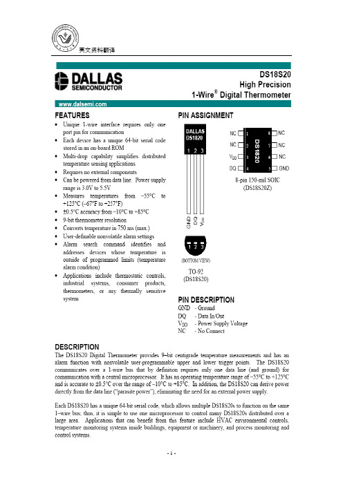
应用范围:包括温度调节装置的控制,工业的系统,消费者产品,温度计, 或任何的热敏感系统管脚描述GND –接地DQ- 数据输入/输出VDD-补给电压收据控制 - 没有连接描述DS18S20 数字温度传感器提供 9 位C数字温度测量而且有一个稳定的用户自定义告警装置,可设计较高和较低的引发点。
DS18S20在一个 1线总线之上数据传送只需要一个数据线 ( 和地线)就可保持与一个中央的微处理器的数据传输。
资讯科技有从 55C到+125 C的温度操作范围而且对从 10C到+85C的的范围内,有0.5 C的温度分辨力。
除此之外, DS18S20的能源供给可直接从数据线获得(寄生功率),而不需要外部的功率供给能源。
每个DS18S20 有独特的 64位序列码, 允许多个 DS18S20s 在同一条1线总线上工作; 因此, 在大的区域使用一个微处理器控制许多 DS18S20s 是方便的。
能受益于这一个特征的应用包括在HVAC环境下的温度控制,在建筑物,仪器或机器里的温度监控系统, 和进程监测控制系统。
概观图 1 所示的是DS18S20的一个块图表,而且管脚的描述表 1也已经给出。
那 64位ROM存储器件有独特的序列编码。
便笺式寄存器包含来自温度传感器的那一片存储器传输出的2个字节的温度记录。
除此之外,便笺式寄存器提供 1字节高位和低位的告警记录(TH 和 TL) 。
DS18B20温度传感器资料
FEATURES Unique 1-Wire interface requires only one port pin for communicationMultidrop capability simplifies distributed temperature sensing applications Requires no external componentsCan be powered from data line. Power supply range is 3.0V to 5.5VZero standby power requiredMeasures temperatures from -55°C to +125°C. Fahrenheit equivalent is -67°F to +257°F±0.5°C accuracy from -10°C to +85°C Thermometer resolution is programmable from 9 to 12 bitsConverts 12-bit temperature to digital word in 750 ms (max.)User-definable, nonvolatile temperature alarm settingsAlarm search command identifies and addresses devices whose temperature is outside of programmed limits (temperature alarm condition)Applications include thermostatic controls,industrial systems, consumer products,thermometers, or any thermally sensitive systemPIN ASSIGNMENTPIN DESCRIPTIONGND - Ground DQ - Data In/OutV DD - Power Supply Voltage NC- No ConnectDESCRIPTIONThe DS18B20 Digital Thermometer provides 9 to 12-bit (configurable) temperature readings which indicate the temperature of the device.Information is sent to/from the DS18B20 over a 1-Wire interface, so that only one wire (and ground)needs to be connected from a central microprocessor to a DS18B20. Power for reading, writing, and performing temperature conversions can be derived from the data line itself with no need for an external power source.Because each DS18B20 contains a unique silicon serial number, multiple DS18B20s can exist on the same 1-Wire bus. This allows for placing temperature sensors in many different places. Applications where this feature is useful include HVAC environmental controls, sensing temperatures inside buildings,equipment or machinery, and process monitoring and control.DS18B20Programmable Resolution 1-Wire ®Digital ThermometerG N D D Q V DDDS18B20 To-92PackageNC NC NC GNDNC NCV DD DQDS18B20Z8-Pin SOIC (150 mil)DETAILED PIN DESCRIPTION Table 1PIN8PIN SOICPINTO92SYMBOL DESCRIPTION51GND Ground.42DQ Data Input/Output pin. For 1-Wire operation: Opendrain. (See “Parasite Power” section.)33V DD Optional V DD pin. See “Parasite Power” section fordetails of connection. V DD must be grounded foroperation in parasite power mode.DS18B20Z (8-pin SOIC): All pins not specified in this table are not to be connected.OVERVIEWThe block diagram of Figure 1 shows the major components of the DS18B20. The DS18B20 has four main data components: 1) 64-bit lasered ROM, 2) temperature sensor, 3) nonvolatile temperature alarm triggers TH and TL, and 4) a configuration register. The device derives its power from the 1-Wire communication line by storing energy on an internal capacitor during periods of time when the signal line is high and continues to operate off this power source during the low times of the 1-Wire line until it returns high to replenish the parasite (capacitor) supply. As an alternative, the DS18B20 may also be powered from an external 3 volt - 5.5 volt supply.Communication to the DS18B20 is via a 1-Wire port. With the 1-Wire port, the memory and control functions will not be available before the ROM function protocol has been established. The master must first provide one of five ROM function commands: 1) Read ROM, 2) Match ROM, 3) Search ROM, 4) Skip ROM, or 5) Alarm Search. These commands operate on the 64-bit lasered ROM portion of each device and can single out a specific device if many are present on the 1-Wire line as well as indicate to the bus master how many and what types of devices are present. After a ROM function sequence has been successfully executed, the memory and control functions are accessible and the master may then provide any one of the six memory and control function commands.One control function command instructs the DS18B20 to perform a temperature measurement. The result of this measurement will be placed in the DS18B20’s scratch-pad memory, and may be read by issuing a memory function command which reads the contents of the scratchpad memory. The temperature alarm triggers TH and TL consist of 1 byte EEPROM each. If the alarm search command is not applied to the DS18B20, these registers may be used as general purpose user memory. The scratchpad also contains a configuration byte to set the desired resolution of the temperature to digital conversion. Writing TH, TL, and the configuration byte is done using a memory function command. Read access to these registers is through the scratchpad. All data is read and written least significant bit first.DS18B20 BLOCK DIAGRAM Figure 1PARASITE POWERThe block diagram (Figure 1) shows the parasite-powered circuitry. This circuitry “steals” power whenever the DQ or V DD pins are high. DQ will provide sufficient power as long as the specified timing and voltage requirements are met (see the section titled “1-Wire Bus System”). The advantages of parasite power are twofold: 1) by parasiting off this pin, no local power source is needed for remote sensing of temperature, and 2) the ROM may be read in absence of normal power.In order for the DS18B20 to be able to perform accurate temperature conversions, sufficient power must be provided over the DQ line when a temperature conversion is taking place. Since the operating current of the DS18B20 is up to 1.5 mA, the DQ line will not have sufficient drive due to the 5k pullup resistor.This problem is particularly acute if several DS18B20s are on the same DQ and attempting to convert simultaneously.There are two ways to assure that the DS18B20 has sufficient supply current during its active conversion cycle. The first is to provide a strong pullup on the DQ line whenever temperature conversions or copies to the E 2 memory are taking place. This may be accomplished by using a MOSFET to pull the DQ line directly to the power supply as shown in Figure 2. The DQ line must be switched over to the strong pull-up within 10 µs maximum after issuing any protocol that involves copying to the E 2 memory or initiates temperature conversions. When using the parasite power mode, the V DD pin must be tied to ground.Another method of supplying current to the DS18B20 is through the use of an external power supply tied to the V DD pin, as shown in Figure 3. The advantage to this is that the strong pullup is not required on the DQ line, and the bus master need not be tied up holding that line high during temperature conversions.This allows other data traffic on the 1-Wire bus during the conversion time. In addition, any number of DS18B20s may be placed on the 1-Wire bus, and if they all use external power, they may all simultaneously perform temperature conversions by issuing the Skip ROM command and then issuing the Convert T command. Note that as long as the external power supply is active, the GND pin may not be floating.The use of parasite power is not recommended above 100°C, since it may not be able to sustain communications given the higher leakage currents the DS18B20 exhibits at these temperatures. For applications in which such temperatures are likely, it is strongly recommended that V DD be applied to the DS18B20.DQVFor situations where the bus master does not know whether the DS18B20s on the bus are parasite powered or supplied with external V DD, a provision is made in the DS18B20 to signal the power supply scheme used. The bus master can determine if any DS18B20s are on the bus which require the strong pullup by sending a Skip ROM protocol, then issuing the read power supply command. After this command is issued, the master then issues read time slots. The DS18B20 will send back “0” on the 1-Wire bus if it is parasite powered; it will send back a “1” if it is powered from the V DD pin. If the master receives a “0,” it knows that it must supply the strong pullup on the DQ line during temperature conversions. See “Memory Command Functions” section for more detail on this command protocol. STRONG PULLUP FOR SUPPLYING DS18B20 DURING TEMPERATURE CONVERSION Figure 2USING V DD TO SUPPLY TEMPERATURE CONVERSION CURRENT Figure 3TO OTHER 1-WIRE DEVICESOPERATION - MEASURING TEMPERATUREThe core functionality of the DS18B20 is its direct-to-digital temperature sensor. The resolution of the DS18B20 is configurable (9, 10, 11, or 12 bits), with 12-bit readings the factory default state. This equates to a temperature resolution of 0.5°C, 0.25°C, 0.125°C, or 0.0625°C. Following the issuance of the Convert T [44h] command, a temperature conversion is performed and the thermal data is stored in the scratchpad memory in a 16-bit, sign-extended two’s complement format. The temperature information can be retrieved over the 1-Wire interface by issuing a Read Scratchpad [BEh] command once the conversion has been performed. The data is transferred over the 1-Wire bus, LSB first. The MSB of the temperature register contains the “sign” (S) bit, denoting whether the temperature is positive or negative.Table 2 describes the exact relationship of output data to measured temperature. The table assumes 12-bit resolution. If the DS18B20 is configured for a lower resolution, insignificant bits will contain zeros. For Fahrenheit usage, a lookup table or conversion routine must be used.Temperature/Data Relationships Table 2232221202-12-22-32-4LSBMSb(unit = °C)LSbS S S S S262524MSBTEMPERATURE DIGITAL OUTPUT(Binary)DIGITAL OUTPUT (Hex)+125°C0000 0111 1101 000007D0h+85°C0000 0101 0101 00000550h*+25.0625°C0000 0001 1001 00010191h+10.125°C0000 0000 1010 001000A2h+0.5°C0000 0000 0000 10000008h0°C0000 0000 0000 00000000h-0.5°C1111 1111 1111 1000FFF8h-10.125°C1111 1111 0101 1110FF5Eh-25.0625°C1111 1110 0110 1111FF6Fh-55°C1111 1100 1001 0000FC90h*The power on reset register value is +85°C.OPERATION - ALARM SIGNALINGAfter the DS18B20 has performed a temperature conversion, the temperature value is compared to the trigger values stored in TH and TL. Since these registers are 8-bit only, bits 9-12 are ignored for comparison. The most significant bit of TH or TL directly corresponds to the sign bit of the 16-bit temperature register. If the result of a temperature measurement is higher than TH or lower than TL, an alarm flag inside the device is set. This flag is updated with every temperature measurement. As long as the alarm flag is set, the DS18B20 will respond to the alarm search command. This allows many DS18B20s to be connected in parallel doing simultaneous temperature measurements. If somewhere the temperature exceeds the limits, the alarming device(s) can be identified and read immediately without having to read non-alarming devices.64-BIT LASERED ROMEach DS18B20 contains a unique ROM code that is 64-bits long. The first 8 bits are a 1-Wire family code (DS18B20 code is 28h). The next 48 bits are a unique serial number. The last 8 bits are a CRC of the first 56 bits. (See Figure 4.) The 64-bit ROM and ROM Function Control section allow the DS18B20 to operate as a 1-Wire device and follow the 1-Wire protocol detailed in the section “1-Wire Bus System.” The functions required to control sections of the DS18B20 are not accessible until the ROM function protocol has been satisfied. This protocol is described in the ROM function protocol flowchart (Figure 5). The 1-Wire bus master must first provide one of five ROM function commands: 1) Read ROM, 2) Match ROM, 3) Search ROM, 4) Skip ROM, or 5) Alarm Search. After a ROM function sequence has been successfully executed, the functions specific to the DS18B20 are accessible and the bus master may then provide one of the six memory and control function commands.CRC GENERATIONThe DS18B20 has an 8-bit CRC stored in the most significant byte of the 64-bit ROM. The bus master can compute a CRC value from the first 56-bits of the 64-bit ROM and compare it to the value stored within the DS18B20 to determine if the ROM data has been received error-free by the bus master. The equivalent polynomial function of this CRC is:CRC = X8 + X5 + X4 + 1The DS18B20 also generates an 8-bit CRC value using the same polynomial function shown above and provides this value to the bus master to validate the transfer of data bytes. In each case where a CRC is used for data transfer validation, the bus master must calculate a CRC value using the polynomial function given above and compare the calculated value to either the 8-bit CRC value stored in the 64-bit ROM portion of the DS18B20 (for ROM reads) or the 8-bit CRC value computed within the DS18B20 (which is read as a ninth byte when the scratchpad is read). The comparison of CRC values and decision to continue with an operation are determined entirely by the bus master. There is no circuitry inside the DS18B20 that prevents a command sequence from proceeding if the CRC stored in or calculated by the DS18B20 does not match the value generated by the bus master.The 1-Wire CRC can be generated using a polynomial generator consisting of a shift register and XOR gates as shown in Figure 6. Additional information about the Dallas 1-Wire Cyclic Redundancy Check is available in Application Note 27 entitled “Understanding and Using Cyclic Redundancy Checks with Dallas Semiconductor Touch Memory Products.”The shift register bits are initialized to 0. Then starting with the least significant bit of the family code, 1 bit at a time is shifted in. After the 8th bit of the family code has been entered, then the serial number is entered. After the 48th bit of the serial number has been entered, the shift register contains the CRC value. Shifting in the 8 bits of CRC should return the shift register to all 0s.64-BIT LASERED ROM Figure 48-BIT CRC CODE48-BIT SERIAL NUMBER 8-BIT FAMILY CODE(28h)MSB LSB MSB LSB MSB LSBROM FUNCTIONS FLOW CHART Figure 51-WIRE CRC CODE Figure 6MEMORYThe DS18B20’s memory is organized as shown in Figure 8. The memory consists of a scratchpad RAM and a nonvolatile, electrically erasable (E 2) RAM, which stores the high and low temperature triggers TH and TL, and the configuration register. The scratchpad helps insure data integrity when communicating over the 1-Wire bus. Data is first written to the scratchpad using the Write Scratchpad [4Eh] command.It can then be verified by using the Read Scratchpad [BEh] command. After the data has been verified, a Copy Scratchpad [48h] command will transfer the data to the nonvolatile (E 2) RAM. This process insures data integrity when modifying memory. The DS18B20 EEPROM is rated for a minimum of 50,000writes and 10 years data retention at T = +55°C.The scratchpad is organized as eight bytes of memory. The first 2 bytes contain the LSB and the MSB of the measured temperature information, respectively. The third and fourth bytes are volatile copies of TH and TL and are refreshed with every power-on reset. The fifth byte is a volatile copy of the configuration register and is refreshed with every power-on reset. The configuration register will be explained in more detail later in this section of the datasheet. The sixth, seventh, and eighth bytes are used for internal computations, and thus will not read out any predictable pattern.It is imperative that one writes TH, TL, and config in succession; i.e. a write is not valid if one writes only to TH and TL, for example, and then issues a reset. If any of these bytes must be written, all three must be written before a reset is issued.There is a ninth byte which may be read with a Read Scratchpad [BEh] command. This byte contains a cyclic redundancy check (CRC) byte which is the CRC over all of the eight previous bytes. This CRC is implemented in the fashion described in the section titled “CRC Generation”.Configuration RegisterThe fifth byte of the scratchpad memory is the configuration register.It contains information which will be used by the device to determine the resolution of the temperature to digital conversion. The bits are organized as shown in Figure 7.DS18B20 CONFIGURATION REGISTER Figure 70R1R011111MSbLSbBits 0-4 are don’t cares on a write but will always read out “1”.Bit 7 is a don’t care on a write but will always read out “0”.R0, R1: Thermometer resolution bits. Table 3 below defines the resolution of the digital thermometer,based on the settings of these 2 bits. There is a direct tradeoff between resolution and conversion time, as depicted in the AC Electrical Characteristics. The factory default of these EEPROM bits is R0=1 and R1=1 (12-bit conversions).Thermometer Resolution Configuration Table 3R1R0Thermometer Resolution Max ConversionTime009 bit 93.75 ms (t conv/8)0110 bit 187.5 ms (t conv /4)1011 bit 375 ms (t conv /2)1112 bit750 ms (t conv )DS18B20 MEMORY MAP Figure 8SCRATCHPADBYTE012345678E 2RAM1-WIRE BUS SYSTEMThe 1-Wire bus is a system which has a single bus master and one or more slaves. The DS18B20 behaves as a slave. The discussion of this bus system is broken down into three topics: hardware configuration, transaction sequence, and 1-Wire signaling (signal types and timing).HARDWARE CONFIGURATIONThe 1-Wire bus has only a single line by definition; it is important that each device on the bus be able to drive it at the appropriate time. To facilitate this, each device attached to the 1-Wire bus must have open drain or 3-state outputs. The 1-Wire port of the DS18B20 (DQ pin) is open drain with an internal circuit equivalent to that shown in Figure 9. A multidrop bus consists of a 1-Wire bus with multiple slaves attached. The 1-Wire bus requires a pullup resistor of approximately 5 kΩ.HARDWARE CONFIGURATION Figure 9The idle state for the 1-Wire bus is high. If for any reason a transaction needs to be suspended, the bus MUST be left in the idle state if the transaction is to resume. Infinite recovery time can occur between bits so long as the 1-Wire bus is in the inactive (high) state during the recovery period. If this does not occur and the bus is left low for more than 480 µs, all components on the bus will be reset. TRANSACTION SEQUENCEThe protocol for accessing the DS18B20 via the 1-Wire port is as follows:InitializationROM Function CommandMemory Function CommandTransaction/DataINITIALIZATIONAll transactions on the 1-Wire bus begin with an initialization sequence. The initialization sequence consists of a reset pulse transmitted by the bus master followed by presence pulse(s) transmitted by the slave(s).The presence pulse lets the bus master know that the DS18B20 is on the bus and is ready to operate. For more details, see the “1-Wire Signaling” section.ROM FUNCTION COMMANDSOnce the bus master has detected a presence, it can issue one of the five ROM function commands. All ROM function commands are 8 bits long. A list of these commands follows (refer to flowchart in Figure 5):Read ROM [33h]This command allows the bus master to read the DS18B20’s 8-bit family code, unique 48-bit serial number, and 8-bit CRC. This command can only be used if there is a single DS18B20 on the bus. If more than one slave is present on the bus, a data collision will occur when all slaves try to transmit at the same time (open drain will produce a wired AND result).Match ROM [55h]The match ROM command, followed by a 64-bit ROM sequence, allows the bus master to address a specific DS18B20 on a multidrop bus. Only the DS18B20 that exactly matches the 64-bit ROM sequence will respond to the following memory function command. All slaves that do not match the 64-bit ROM sequence will wait for a reset pulse. This command can be used with a single or multiple devices on the bus.Skip ROM [CCh]This command can save time in a single drop bus system by allowing the bus master to access the memory functions without providing the 64-bit ROM code. If more than one slave is present on the bus and a Read command is issued following the Skip ROM command, data collision will occur on the bus as multiple slaves transmit simultaneously (open drain pulldowns will produce a wired AND result). Search ROM [F0h]When a system is initially brought up, the bus master might not know the number of devices on the 1-Wire bus or their 64-bit ROM codes. The search ROM command allows the bus master to use a process of elimination to identify the 64-bit ROM codes of all slave devices on the bus.Alarm Search [ECh]The flowchart of this command is identical to the Search ROM command. However, the DS18B20 will respond to this command only if an alarm condition has been encountered at the last temperature measurement. An alarm condition is defined as a temperature higher than TH or lower than TL. The alarm condition remains set as long as the DS18B20 is powered up, or until another temperature measurement reveals a non-alarming value. For alarming, the trigger values stored in EEPROM are taken into account. If an alarm condition exists and the TH or TL settings are changed, another temperature conversion should be done to validate any alarm conditions.Example of a ROM SearchThe ROM search process is the repetition of a simple three-step routine: read a bit, read the complement of the bit, then write the desired value of that bit. The bus master performs this simple, three-step routine on each bit of the ROM. After one complete pass, the bus master knows the contents of the ROM in one device. The remaining number of devices and their ROM codes may be identified by additional passes.The following example of the ROM search process assumes four different devices are connected to the same 1-Wire bus. The ROM data of the four devices is as shown:ROM100110101...ROM210101010...ROM311110101...ROM400010001...The search process is as follows:1.The bus master begins the initialization sequence by issuing a reset pulse. The slave devices respondby issuing simultaneous presence pulses.2.The bus master will then issue the Search ROM command on the 1-Wire bus.3.The bus master reads a bit from the 1-Wire bus. Each device will respond by placing the value of thefirst bit of their respective ROM data onto the 1-Wire bus. ROM1 and ROM4 will place a 0 onto the 1-Wire bus, i.e., pull it low. ROM2 and ROM3 will place a 1 onto the 1-Wire bus by allowing the line to stay high. The result is the logical AND of all devices on the line, therefore the bus master sees a 0. The bus master reads another bit. Since the Search ROM data command is being executed, all of the devices on the 1-Wire bus respond to this second read by placing the complement of the first bit of their respective ROM data onto the 1-Wire bus. ROM1 and ROM4 will place a 1 onto the 1-Wire, allowing the line to stay high. ROM2 and ROM3 will place a 0 onto the 1-Wire, thus it will be pulled low. The bus master again observes a 0 for the complement of the first ROM data bit. The bus master has determined that there are some devices on the 1-Wire bus that have a 0 in the first position and others that have a 1.The data obtained from the two reads of the three-step routine have the following interpretations:00There are still devices attached which have conflicting bits in this position.01All devices still coupled have a 0-bit in this bit position.10All devices still coupled have a 1-bit in this bit position.11There are no devices attached to the 1-Wire bus.4.The bus master writes a 0. This deselects ROM2 and ROM3 for the remainder of this search pass,leaving only ROM1 and ROM4 connected to the 1-Wire bus.5.The bus master performs two more reads and receives a 0-bit followed by a 1-bit. This indicates thatall devices still coupled to the bus have 0s as their second ROM data bit.6.The bus master then writes a 0 to keep both ROM1 and ROM4 coupled.7.The bus master executes two reads and receives two 0-bits. This indicates that both 1-bits and 0-bitsexist as the 3rd bit of the ROM data of the attached devices.8.The bus master writes a 0-bit. This deselects ROM1, leaving ROM4 as the only device stillconnected.9.The bus master reads the remainder of the ROM bits for ROM4 and continues to access the part ifdesired. This completes the first pass and uniquely identifies one part on the 1-Wire bus.10.The bus master starts a new ROM search sequence by repeating steps 1 through 7.11.The bus master writes a 1-bit. This decouples ROM4, leaving only ROM1 still coupled.12.The bus master reads the remainder of the ROM bits for ROM1 and communicates to the underlyinglogic if desired. This completes the second ROM search pass, in which another of the ROMs was found.13.The bus master starts a new ROM search by repeating steps 1 through 3.14.The bus master writes a 1-bit. This deselects ROM1 and ROM4 for the remainder of this search pass,leaving only ROM2 and ROM3 coupled to the system.15.The bus master executes two Read time slots and receives two 0s.16.The bus master writes a 0-bit. This decouples ROM3 leaving only ROM2.17.The bus master reads the remainder of the ROM bits for ROM2 and communicates to the underlyinglogic if desired. This completes the third ROM search pass, in which another of the ROMs was found.18.The bus master starts a new ROM search by repeating steps 13 through 15.19.The bus master writes a 1-bit. This decouples ROM2, leaving only ROM3.20.The bus master reads the remainder of the ROM bits for ROM3 and communicates to the underlyinglogic if desired. This completes the fourth ROM search pass, in which another of the ROMs was found.NOTE:The bus master learns the unique ID number (ROM data pattern) of one 1-Wire device on each ROM Search operation. The time required to derive the part’s unique ROM code is:960 µs + (8 + 3 x 64) 61 µs = 13.16 msThe bus master is therefore capable of identifying 75 different 1-Wire devices per second.I/O SIGNALINGThe DS18B20 requires strict protocols to insure data integrity. The protocol consists of several types of signaling on one line: reset pulse, presence pulse, write 0, write 1, read 0, and read 1. All of these signals, with the exception of the presence pulse, are initiated by the bus master.The initialization sequence required to begin any communication with the DS18B20 is shown in Figure 11. A reset pulse followed by a presence pulse indicates the DS18B20 is ready to send or receive data given the correct ROM command and memory function command.The bus master transmits (TX) a reset pulse (a low signal for a minimum of 480 µs). The bus master then releases the line and goes into a receive mode (RX). The 1-Wire bus is pulled to a high state via the 5k pullup resistor. After detecting the rising edge on the DQ pin, the DS18B20 waits 15-60 µs and then transmits the presence pulse (a low signal for 60-240 µs).MEMORY COMMAND FUNCTIONSThe following command protocols are summarized in Table 4, and by the flowchart of Figure 10.Write Scratchpad [4Eh]This command writes to the scratchpad of the DS18B20, starting at the TH register. The next 3 bytes written will be saved in scratchpad memory at address locations 2 through 4. All 3 bytes must be written before a reset is issued.Read Scratchpad [BEh]This command reads the contents of the scratchpad. Reading will commence at byte 0 and will continue through the scratchpad until the ninth (byte 8, CRC) byte is read. If not all locations are to be read, the master may issue a reset to terminate reading at any time.Copy Scratchpad [48h]This command copies the scratchpad into the E2memory of the DS18B20, storing the temperature trigger bytes in nonvolatile memory. If the bus master issues read time slots following this command, the DS18B20 will output 0 on the bus as long as it is busy copying the scratchpad to E2; it will return a 1 when the copy process is complete. If parasite-powered, the bus master has to enable a strong pullup for at least 10 ms immediately after issuing this command. The DS18B20 EEPROM is rated for a minimum of 50,000 writes and 10 years data retention at T=+55°C.Convert T [44h]This command begins a temperature conversion. No further data is required. The temperature conversion will be performed and then the DS18B20 will remain idle. If the bus master issues read time slots following this command, the DS18B20 will output 0 on the bus as long as it is busy making a temperature conversion; it will return a 1 when the temperature conversion is complete. If parasite-powered, the bus master has to enable a strong pullup for a period greater than t conv immediately after issuing this command.Recall E2 [B8h]This command recalls the temperature trigger values and configuration register stored in E2 to the scratchpad. This recall operation happens automatically upon power-up to the DS18B20 as well, so valid data is available in the scratchpad as soon as the device has power applied. With every read data time slot issued after this command has been sent, the device will output its temperature converter busy flag: 0=busy, 1=ready.Read Power Supply [B4h]With every read data time slot issued after this command has been sent to the DS18B20, the device will signal its power mode: 0=parasite power, 1=external power supply provided.。
温度测量(ds18b20)
用DS18B20温度传感器进行温度测量DALLAS最新单线数字温度传感器DS18B20简介新的“一线器件”体积更小、适用电压更宽、更经济Dallas 半导体公司的数字化温度传感器DS1820是世界上第一片支持“一线总线”接口的温度传感器。
一线总线独特而且经济的特点,使用户可轻松地组建传感器网络,为测量系统的构建引入全新概念。
DS18B20、DS1822 “一线总线”数字化温度传感器同DS1820一样,DS18B20也支持“一线总线”接口,测量温度范围为-55°C~+125°C,在-10~+85°C范围内,精度为±0.5°C。
DS1822的精度较差为±2°C 。
现场温度直接以“一线总线”的数字方式传输,大大提高了系统的抗干扰性。
适合于恶劣环境的现场温度测量,如:环境控制、设备或过程控制、测温类消费电子产品等。
与前一代产品不同,新的产品支持3V~5.5V的电压范围,使系统设计更灵活、方便。
而且新一代产品更便宜,体积更小。
DS18B20、DS1822 的特性DS18B20可以程序设定9~12位的分辨率,精度为±0.5°C。
可选更小的封装方式,更宽的电压适用范围。
分辨率设定,及用户设定的报警温度存储在EEPROM中,掉电后依然保存。
DS18B20的性能是新一代产品中最好的!性能价格比也非常出色!DS1822与DS18B20软件兼容,是DS18B20的简化版本。
省略了存储用户定义报警温度、分辨率参数的EEPROM,精度降低为±2°C,适用于对性能要求不高,成本控制严格的应用,是经济型产品。
继“一线总线”的早期产品后,DS1820开辟了温度传感器技术的新概念。
DS18B20和DS1822使电压、特性及封装有更多的选择,让我们可以构建适合自己的经济的测温系统。
DS18B20的内部结构DS18B20内部结构主要由四部分组成:64位光刻ROM、温度传感器、非挥发的温度报警触发器TH和TL、配置寄存器。
温度传感器(DS18B20)工作原理及应用
Copy Scratchpad(复制暂存存储器)[48h]
这条命令把暂存器的内容拷贝到DS18B20的E2存储 器里,即把温度报警触发字节存入非易失性存储器 里。如果总线控制器在这条命令之后跟着发出读时 间隙,而DS18B20又正在忙于把暂存器拷贝到E2存 储器,DS18B20就会输出一个“0”,如果拷贝结束 的话,DS18B20 则输出“1”。如果使用寄生电源, 总线控制器必须在这条命令发出后立即起动强上拉 并最少保持10ms。
Convert T(温度变换)[44h]
这条命令启动一次温度转换而无需其他数据。温度 转换命令被执行,而后DS18B20保持等待状态。如 果总线控制器在这条命令之后跟着发出读时间隙, 而DS18B20又忙于做时间转换的话,DS18B20将在 总线上输出“0”,若温度转换完成,则输出“1”。如 果使用寄生电源,总线控制器必须在发出这条命令 后立即起动强上拉,并保持500ms。
(1)初始化 单总线上的所有处理均从初始化序列开始。初 始化序列包括
总线主机发出一复位脉冲 接着由从属器件送出存在脉冲。存在脉冲让总线控 制器知道DS1820 在总线上且已准备好操作。
每一次通信之前必须进行复位,复位的时间、等待 时间、回应时间应严格按时序编程。
初始化C语言程序 sbit DQ=P3^3; void Delay(uint x) { while(--x); }
(2)DS18B20的RAM及EEPROM
RAM 数据暂存器,用于内部计算和数据存取,数据在
掉电后丢失,DS18B20共9个字节RAM,每个字节为8位。 第1、2个字节是温度转换后的数据值信息, 第3、4个字节是用户EEPROM(常用于温度报警值储存) 的镜像。在上电复位时其值将被刷新。 第5个字节则是用户第3个EEPROM的镜像。 第6、7、8个字节为计数寄存器,是为了让用户得到更高的 温度分辨率而设计的,同样也是内部温度转换、计算的暂 存单元。 第9个字节为前8个字节的CRC码。 EEPROM 非易失性记忆体,用于存放长期需要保存的数据, 上下限温度报警值和校验数据,DS18B20共3位EEPROM, 并在RAM都存在镜像,以方便用户操作。
外文资料翻译---智能温度传感器DS18B20的原理及其应用
外文资料翻译资料来源:第七届国际测试技术研讨会文章名:The Principle of the Intelligent Temperature Sensor DS18B20and Its Application作者:LI Shuo LI Xiaomi文章译名:智能温度传感器DS18B20的原理与测量姓名:学号:指导教师(职称):专业:班级:所在学院:译文智能温度传感器DS18B20的原理及其应用摘要:功能和结构的数字本文介绍了温度测量芯片DS18B20的温度测量系统的介绍,8051单片机作为其作品CPU和DALLAS18B20其温度数据收集 - 转换。
硬件的原理,软件程图和一个短暂的时间延迟子程序也都给予列出。
关键词:DS18B20温度传感器,单片机微机,硬件设计一、导言单轨数字温度传感器DS18B20的生产由美国DALLAS公司。
它可以转换的温度信号成字信号提供的微电脑处理直接。
与传统的相比热敏电阻器,它可以直接读出的措施温度并根据实际它可以actualize 9〜12的数值读数方式通过简单的编程。
信息读取或写入DS18B20的,只需要一个单一的线。
温度变换功率来源于为主线,主线本身可以供电源DS18B20的,不需要额外的电源。
因此,如果使用DS18B20的,系统的结构会更简单,更可靠。
因为每个DS18B20包含一个独特的硅序列号,多个DS18B20s 可以存在于相同的1-Wire总线。
这允许浇筑温度传感器在许多不同的地方。
应用场合此功能是有用的,包括HVAC环境控制,检测建筑物内的温度,设备或机械,过程监测和控制。
二、 DS18B20的结构DS18B20的四个组成部分的主要数据:(1)64位光刻ROM(2)温度传感器(3)非易失性温度报警触发器TH和TL(4)配置寄存器。
设备源于其权力从1-Wire通信线通过储能在一段时间的内部电容当信号线为高,并继续操作此期间的低倍的电源关闭1-Wire线,直到它返回来补充高寄生虫(电容器)供应。
- 1、下载文档前请自行甄别文档内容的完整性,平台不提供额外的编辑、内容补充、找答案等附加服务。
- 2、"仅部分预览"的文档,不可在线预览部分如存在完整性等问题,可反馈申请退款(可完整预览的文档不适用该条件!)。
- 3、如文档侵犯您的权益,请联系客服反馈,我们会尽快为您处理(人工客服工作时间:9:00-18:30)。
Student ID : 201710319
NAME: MengYang
一、DESCRIPTION:
DS18B20 is a first-line digital temperature sensor produced by Dallas company. The DS18B20 digital thermometer provides 9-bit to 12-bit Celsius temperature measurements and has an alarm function with nonvolatile user-programmable upper and lower trigger points. The DS18B20 communicates over a 1-Wire bus that by definition requires only one data line (and ground) for communication with a central microprocessor. It has an operating temperature range of -55°C to +125°C and is accurate to ±0.5°C over the range of -10°C to +85°C. In addition, the DS18B20 can derive power directly from the data line (“parasite power”), eliminating the need for an external power supply.
二、FEATURES:
1.Can Be Powered from Data Line; Power Supply Range is 3.0V to
5.5V.
2.Measures Temperatures from -55°C to +125°C (-67°F to +257°F)
3.±0.5°C Accuracy from -10°C to +85°C.
4.Thermometer Resolution is User Selectable from 9 to 12 Bits.
5.Converts Temperature to 12-Bit Digital Word in 750ms (Max).
6.Each Device has a Unique 64-Bit Serial Code Stored in an On-Board
ROM
7.Another feature of the DS18B20 is the ability to operate without an
external power supply. Power is instead supplied through the 1-Wire pullup resistor via the DQ pin when the bus is high. The high bus signal also charges an internal capacitor (CPP), which then supplies power to the device when the bus is low.
三、Application scope:
The product is suitable for temperature measurement and control fields such as freezer, granary, storage tank, telecommunication room, power room, cable trough, etc.
四、Wiring method
Facing the flat side, the left side is negative and the right side is positive. If it is reversed, it will immediately heat up and may burn! At the same time, the reverse connection is also the reason why the sensor always displays 85 ℃. In the actual operation, the positive and negative will be reversed, the sensor will immediately heat up, the LCD screen can
not display the reading, after the positive and negative are connected, the display will be 85 ℃. In addition, if 51 single chip microcomputer is used, then the middle pin must be connected with a 4.7k-10k pull-up resistor, otherwise, because the high level cannot be normally input / output, either 85 ℃will be displayed immediately after power on, or the temperature will jump on the normal value at 85 ℃after several months.。