dc-dc XR8505 5V3A车充 规格书
5V1.5A旅充承认书(DC2.5)欧规
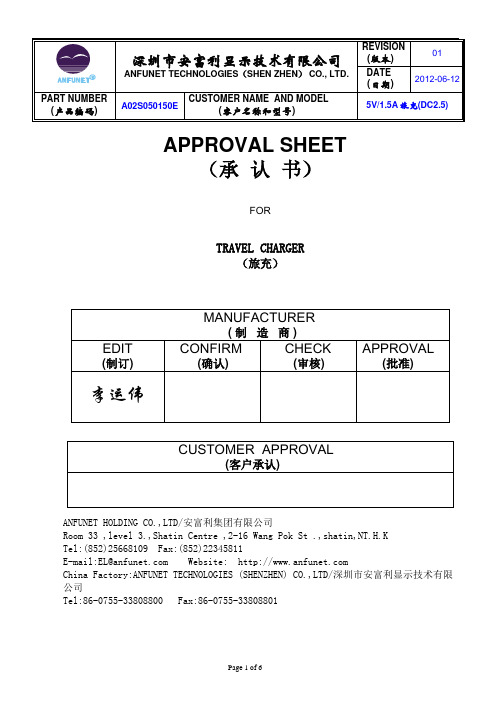
APPROVAL SHEET(承认书)FORTRAVEL CHARGER(旅充)ANFUNET HOLDING CO.,LTD/安富利集团有限公司Room 33 ,level 3.,Shatin Centre ,2-16 Wang Pok St .,shatin,NT.H.KTel:(852)25668109 Fax:(852)22345811E-mail:EL@ Website: China Factory:ANFUNET TECHNOLOGIES (SHENZHEN) CO.,LTD/深圳市安富利显示技术有限公司Tel:86-0755-******** Fax:86-0755-********1. Apply Scope(适用范围)This specification shall be applied to car charger 5V/1.5A本规格适用于5V/1.5A旅充。
2. INPUT REQUIREMENTS(输入要求)Regular input voltage/额定输入电压:AC100-AC240VRating frequency/额定输入频率:50HZ/60HZInput current/输入电流:0.3Arms MAX(at regular input voltage£ rating output current) 最大电流0.3A(额定输入电压及输入电流)3. INRUSH CURRENT(浪涌电流)40A max at 240V ac input for a cold start at 25℃.在冷机25℃时开机输入240V AC 最大浪涌电流40A.4. STANDBY-POWER CONSUMPTION(能量消耗)This S.M.P.S standby power consumption 0.8W Max.这个电源供应器空载时最大功耗最大0.8 W5. Output Characteristics(输出特性)Output Voltage /输出电压.No load voltage /空载输出电压:DC5.0V-5.4VFull load voltage /满载输出电压:DC 4.5V-5.3 VRated Output Current (额定输出电流)±10%The output current will be performed from 1.5A(额定输出电流1.5A )Rated Power (额定功率)±10%The rated power is7.5Watts.(输出功率7.5Watts )Protection (保护)Short Circuit Protection (短路保护)The charger is protected that a short happened between the output terminals and shall not result in a fire hazard, any damage to this Charger and will be normal operation automatically while the short is removed.(输出短路后不损坏该制品,短路恢复正常输出,)6. Mechanical Features(外形尺寸图)欧规外壳(不带灯孔不印字)尺寸:41.5mm*70mm*44.5mm7. Rating Label Drawing(标贴纸图)8. The DC line size diagram(DC线尺寸图) (1) DC2.59. Packing Drawing(装箱图)。
RCS-9785CD_X_说明书_国内中文_国内标准版_X_R1.02_(ZL_TXZZ0163.1208)
危险!
意味着如果安全预防措施被忽视,则会导致人员死亡 , 严重的人身伤害,或
严重的设备损坏。 警告! 意味着如果安全预防措施被忽视,则可能导致人员死亡 , 严重的人身伤害,
或严重的设备损坏。 警示! 意味着如果安全预防措施被忽视,则可能导致轻微的人身伤害或设备损坏。
本条特别适用于对装置的损坏及可能对被保护设备的损坏。 警告! 为增强或修改现有功能,装置的软硬件均可能升级,请确认此版本的使用手册和您手中的产品 兼容。 警告! 电气设备在运行时,这些装置的某些部件可能带有高压。不正确的操作可能导致严重的人身伤 害或设备损坏。 只有具备资质的合格专业工作人员才允许对装置或在装置临近工作。工作人员需熟知本手册中 所提到的注意事项和工作流程,以及安全规定。 特别注意,一些通用的工作于高压带电设备的工作规则必须遵守。如果不遵守可能导致严重的 人身伤亡或设备损坏。 警告! 曝露端子 在装置带电时不要触碰曝露的端子等,因为可能会产生危险的高电压。 残余电压
RCS-9785C/D GPS 时钟同步装置 说明书
ii
南京南瑞继保电气有限公司
RCS-9785C/D GPS 时钟同步装置
前言 使用产品前,请仔细阅读本章节!
本章叙述了使用产品前的安全预防建议。在安装和使用时,本章内容必须全部阅读且充分理解。 忽略说明书中相关警示说明,因不当操作造成的任何损害,我公司不承担相应负责。 在对本装置做任何操作前,相关专业人员必须仔细阅读本说明书,熟悉操作相关内容。 操作指导及警告 本手册中将会用到以下指示标记和标准定义:
ii
南京南瑞继保电气有限公司
RCS-9785C/D GPS 时钟同步装置
目录
前言........................................................................................................................................i 目录..................................................................................................................................... iii 第 1 章 概述 ....................................................................................................................... 1 1.1 应用 ....................................................................................................................... 1 1.2 功能 ....................................................................................................................... 1 1.3 特点 ....................................................................................................................... 2 1.4 订货选型 ................................................................................................................ 2 1.5 产品执行标准 ......................................................................................................... 2 第 2 章 技术参数 ............................................................................................................... 3 2.1 通用技术参数 ......................................................................................................... 3 2.1.1 电气参数 ...................................................................................................... 3 2.1.2 机械特性 ...................................................................................................... 3 2.1.3 环境条件参数 .............................................................................................. 4 2.1.4 对时接口参数 .............................................................................................. 4 2.1.5 型式试验参数 .............................................................................................. 5 2.2 时间同步参数 ......................................................................................................... 6 2.2.1 1PPS 脉冲.................................................................................................... 6 2.2.2 1PPM 脉冲 ................................................................................................... 7 2.2.3 1PPH 脉冲 ................................................................................................... 7 2.2.4 IRIG-B DC 码 ............................................................................................... 7 2.2.5 IRIG-B AC 码 ............................................................................................... 7 2.2.6 串口对时报文 .............................................................................................. 7 2.2.7 GPS 接收模块 .............................................................................................. 8 2.2.8 北斗接收模块 .............................................................................................. 8 2.2.9 内部守时时钟 .............................................................................................. 8 2.3 认证 ....................................................................................................................... 8 第 3 章 工作原理 ................................................................................................................ 9 第 4 章 硬件描述 ............................................................................................................... 11
IMAX充电器说明
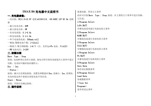
IMAX B6 充电器中文说明书一.充电器参数:—电压值:DC11.0-18.0V 选配AC100-240, -50/60HZ 12V DC 5A 适配器—最大充电功率:50W—最大放电功率:5W—充电电流值:0.1-5.0A—放电电流值:0.1-1.0A—单个电池的电流:300mah/cell—镍氢/镍镉电池个数:1-15cell—锂离子/聚合物级数:1-6节(注:支持Li-Fe电池,即A123)—PB电池电压:2-20V二.按键功能Batt. Type / Stop按钮:电池种类以及停止按钮,接电后即可使用该按钮在主菜单中进行切换,充电时可随时按此键停止;Dec. / Inc.< Status >按钮:减小以及增加按钮,设置各种数值时Dec.是减小,Inc.是增加,充电时按这两个按钮以浏览电池不同信息;Start / Enter按钮:开始以及确定按钮。
三.操作说明接通电源,即显示主菜单此时可以按Batt. Type / Stop 按钮,在主要的几个菜单中进行切换,它们是:1)Program SelectLiPo BATT对锂电池系列进行充放电的主菜单2)Program SelectMiMH BATT对镍氢电池进行充放电的主菜单3)Program SelectNiCd BATT对镍镉电池进行充放电的主菜单4)Program SelectPb BATT对蓄电池进行充放电的主菜单5)Program SelectSave Data保存设定数据菜单6)Program SelectLoad Data加载数据菜单7)User SetProgram->使用者设定菜单四、锂电池充放电1.)充电开机后显示主菜单:Program SelectLiPo BATT按Start / Enter按钮确定屏幕显示LiPo CHARGE*.*A *.*V(*S)这个是锂电充电,非平衡充,不推荐所以要继续.(适用于不带平衡端子的锂电池)按Inc. >,屏幕显示:LiPo BALANCE*.*A *.*V(*S)这个就是锂电平衡充电功能了,我们模型基本要用的就是平衡充电,所以要在这里进行操作,如下:按Start / Enter,A前面的数字闪烁按Dec. <或者Inc. >改变改数值大小,这个是充电电流选择,锂聚合物电池最多不可超过1c,也就是4400mah电池最高用4.4a,2200mah 电池最高用2.2a,这样类推;建议保守点用0.5c,即4400mah电池用2.2a,依此类推Dec. <减小该数值,Inc. >增加该数值按Start / Enter,V(*S)前面的数字闪烁按Dec. <或者Inc. >改变改数值大小,这个是选择电池额定电压,为3.7的倍数,车用电池一般为7.4v,即2S(每3.7v=1S)长按Start / Enter,出现如下屏幕:Battery CheckWait…如果电池连接不正确,则显示:CONNECTION BREAK如连接正确,则显示:上行:R: *SER S: *SER(说明一下:R: *SER是指充电器自动检测到的电池节数,S: *SER是你设置的电池节数,如果数值不等,请不要开始充电,以免损坏电池)下行:CANCEL(STOP)与CONFIRM(ENTER)来回切换此时按Start / Enter开始充电,按Satt. Type / Stop取消充电,返回设置界面充电界面:Li*S *.*A *.**VCHG ***:** *****第一行:锂电节数,即时充电电流,即时电池总电压第二行:充电指示,充电耗时,充进的电量充电指示:充电时显示CHG , 充满之后显示:FULL***充电过程中可随时按Batt. Type / Stop按钮停止充电***充电过程中壳随时按Start / Enter按钮改变充电电流,改变后记得再次确认即可***充电过程中可随时按 Inc. > 观看各节电池单独电压***充电过程中可随时按 Dec. < 观看各设定参数2.)放电在对锂电池系列进行充放电的主菜单中继续按Inc. > ,屏幕显示如下界面:LiPo DISCHARGE*.*A *.*V(*S)按Start / Enter,选择\放电功能,操作方法跟充电一样,设置好放电电流和放电截至电压即可,电压为3的倍数级增减,7.4v锂电请设为6.0V(2S)***注意:必须同时接上放电接头以及平衡充电接头,方可进行对锂电的充放***补充:LiPoCHARGE / LiPo FAST CHG具体作用,适用于不带平衡端子的锂聚合物电池充电/锂聚合物快速充电,对于有平衡端的电池不建议使用。
XL1507 150KHz 40V 3A开关电流降压型DC-DC转换器说明书

150KHz 40V 3A开关电流降压型DC-DC转换器XL1507特点⏹ 4.5V到40V宽输入电压范围⏹输出版本固定5V和ADJ可调⏹输出电压1.23V到37V可调⏹最大占空比100%⏹最小压差1.5V⏹固定150KHz开关频率⏹最大3A开关电流⏹内置功率三极管⏹高效率⏹出色的线性与负载调整率⏹EN脚TTL关机功能⏹EN脚迟滞功能⏹内置热关断功能⏹内置限流功能⏹内置二次限流功能⏹TO252-5L封装应用⏹LCD电视与显示屏⏹数码相框⏹机顶盒⏹路由器⏹通讯设备供电描述XL1507是一款高效降压型DC-DC转换器,固定150KHz开关频率,可以提供最高3A输出电流能力,具有低纹波,出色的线性调整率与负载调整率特点。
XL1507内置固定频率振荡器与频率补偿电路,简化了电路设计。
PWM控制环路可以调节占空比从0~100%之间线性变化。
内置使能功能、输出过电流保护功能。
当二次限流功能启用时,开关频率从150KHz降至50KHz。
内部补偿模块可以减少外围元器件数量。
图1.XL1507封装150KHz 40V 3A 开关电流降压型DC-DC 转换器 XL1507引脚配置EN GND SW VINFB 12345TO252-5LMetal Tab GND图2. XL1507引脚配置表1.引脚说明引脚号 引脚名称 描述1 VIN 电源输入引脚,支持DC4.5V~40V 宽范围电压操作,需要在VIN 与GND 之间并联电解电容以消除噪声。
2 SW 功率开关输出引脚,SW 是输出功率的开关节点。
3 GND 接地引脚。
4 FB 反馈引脚,通过外部电阻分压网络,检测输出电压进行调整,参考电压为1.23V 。
5 EN使能引脚,低电平工作,高电平关机,悬空时为低电平。
150KHz 40V 3A 开关电流降压型DC-DC 转换器 XL1507方框图EA1.23V ReferenceGNDFB3.3V 1.23VEA COMPOscillator 150KHz3.3V Regulator Start UpLatchCOMP2COMP1DriverThermal ShutdowninENSW220mV 200mV44m ΩCurrent LimitR2R1=2.5K5V R2=7.6KADJ R2=0 R1=OPENSwitch图3. XL1507方框图典型应用XL1507-5.0CIN 470uf 35VC1 105330uf 35VD1 L1 33uh/3A+12VLOAD13524GNDVINFBSWEN ON OFF 5V/3ACOUT 1N5820图4. XL1507系统参数测量电路(12V-5V/3A )150KHz 40V 3A 开关电流降压型DC-DC 转换器 XL1507订购信息产品型号 打印名称封装方式包装类型 XL1507-ADJE1 XL1507-ADJE1 TO252-5L 2500只每卷 XL1507-5.0E1 XL1507-5.0E1TO252-5L2500只每卷XLSEMI 无铅产品,产品型号带有“E1”后缀的符合RoHS 标准。
同步降压DC-DC cx8505

一、 概述是一款单芯片的同步降压稳压器。
在输入电压范围内可提供持续的3A 负载电流,采用的电流控制模式有快的瞬态响应和不间断的过流检测,具有软启动、低压保护、过温保护、过流保护等功能,在待机模式下电流仅为0.3μA 。
二、 应用领域分布式电源系统 网络系统 笔记本电脑三、 特点3A 输出电流、4A 峰值电流输入电压范围4.75V~ V内部集成功率MOSFET 开关管 输出电压在0.925V ~20V 间可调 高达95%的效率 可调整的软启动时间四、 极限参数名称 符号 参数 输入电压 V IN -0.3V开关节点电压 V SW 21V充电电压 V BS V SW - 0.3~V SW +6V其它管脚 -0.3V ~6V 焊接温度 260°C 储存温度–65°C ~ +150°CCX850530~30VIC源厂 贺 137 2557 1873五、 典型工作条件名称 符号 参数 输入电压 V IN 4.75V ~ V输出电压 V OUT 0.925V~20V 环境温度T–40°C ~ +85°C六、 内部框图七、 管脚定义管脚 名称 描述 1 BS 上管驱动栅极输入端,在BS 和SW 之间连接一个0.01μF 或更大的电容,充电升压后为上管(N 沟道MOSFET )提供驱动。
2 IN 电源输入端。
为IC 和降压稳压器提供4.75V~18V 的电源,在输入和地之间接一个合适大小的旁路电容,减少输入到IC 的噪声。
3 SW 功率开关管输出端。
这个开关节点为输出提供能量,将LC 滤波器连接在SW 和输出端。
注意需要BS 和SW 之间的升压电容驱动开关管。
4 GND 地。
5 FB 反馈输入端。
输出端经过电阻分压后提供给FB 的输入,通过这个采样反馈来调节输出电压,反馈端的比较点为0.925V 。
6 COMP 补偿端。
在COMP 和地之间的串联RC 网络被用来补偿系统的闭环控制,一些情况下需要在COMP 和地之间再加一个电容。
ENERMAX Revolution XT 860W 850W 800W 750W 电源手册说明书
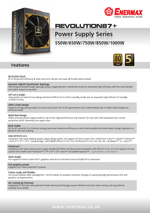
o w e r S u p p l y S e r i e sPower Supply Series80 PLUS® GOLD87to93percenteffi***************************************®Goldcertified.Dynamic Hybrid Transformer TopologyTechnological breakthrough topology using a staged dynamic transformer array for extremely high efficiency with the most durable and stable output at any load.ErP Lot 6 ready!Help systems to meet EU eco-design directive ErP/EuP Lot 6 (<1W in standby mode) due to improved, high-efficient 5V standby(+5Vsb) circuitry.ZERO LOAD DesignSupports energy saving modes of current and future CPU & GPU generations (C6 & Hybrid Mode) due to ZERO LOAD Design (no minimum load).Multi-Rail-DesignStable and safe power supply thanks to up to four high-performance and massive 12V rails each with separated over current protection (OCP). Extremely low ripple noise.Rock StableDC-to-DC converter for minimum energy losses and maximum efficiency as well as best possible and most stable voltage regulation at dynamic and cross loading.Intel ATX12V v2.3Compliant with latest desktop power supply design guide. Full support of most current CPU: Intel® Core 2 Duo™ / Quad™ / Extreme™ / Core i7™ / i5™ / i3™, “Sandy Bridge“ and AMD® Athlon™ II X2 / X3 / X4 Phenom™ II X2 / X3 / X4 / X6, …Bulldozer™“ or “Llano™“.Fit4Server*Compliant with latest server power supply standard SSI PSDG and downward compatible with EPS12V v2.92, v2.8. Full support of most current CPU Intel® Core™ Extreme™ / i7™ / i5™ / i3™, Xeon™ and AMD® Opteron™. * only ERV850EWT-G and ERV1000EWT-GDXXI ready!Full support of most current DX11 graphics cards due to minimum two 6+2P (8P) PCI-E connectors.Full graphics powerSupports SLI™ and CrossFireX™ systems.Future ready and flexibleAll-round modular cable management. 10/12P sockets for possible connector changes of upcoming high-performance CPU and graphics card generations.Air Cooling by EnermaxIntegrated 13.9cm fan with patented Twister Bearing Technology ensures efficient and ultra silent cooling and long lifetime(100,000 hours MTBF).550W/650W/750W/850W/1000W50W/650W/750W/850W/1000W550W/650W/750W/850W/1000PFeatures5FeaturesCables & ConnectorsSpeedGuardUltra silent and powerful cooling performance thanks to the advanced and intelligent fuzzy logic fan speed control with min. 300 or 500 RPM up to max. 1,000 or 1,200 RPM (depending on the model).HeatGuardKeeping PSU fan running for 30-60 seconds after shut down to dissipate the remaining system heat and prolonging system lifetime.SafeGuardIndustry-leading multiple protection circuitry of OCP , OVP , UVP , OPP , OTP , SCP & SIP .CordGuardFixing the AC cord tightly to avoid accidental shutdowns of your PC.Non-stop @ 50°CNon-Stop industrial class performance at 50°C ambient.High-quality Japanese CapacitorsHighest Enermax quality standards for leading stability and maximum durability. 105°C Japanese electrolytic capacitors without exception.Worldwide Compatibility100-240V AC* input with automatic adjustment and up to 99% active Power Factor Correction (PFC) for global usage.* ERV1000EWT -G: 115-240VENERGY STAR 5.0 ready!Support computer system to meet ENERGY STAR 5.0 standard.Dimensions (W x H x D)550/650W: 150mm x 86mm x 160mm750/850/1000W: 150mm x 86mm x 175mmWarranty 5 years vendor warranty.ERV 550AWT -GERV 650AWT -GERV 750AWT -GERV 850EWT -GERV 1000EWT -G(f)=fixed cables; (m)=modular cablesModular cabelERVERV ERV ERV ERV Cables & ConnectorsSpecificationsERVERV ERV ERV ERVThe latest graphics cards and processors are equipped with energy-saving functions that work extremely efficient at low load aswell as in idle mode.These energy saving functions are a big challenge for power supplies. Only few can work stable at loads below 1W. They shut down or react with an unstable power supply. Enermax power supplies with ZERO LOAD Design are well prepared for the energy saving modes of modern graphics cards and processors. Even at a load below 1W, they can provide rock stable voltages.(so-called Deep Power Down): At idle mode, modern multi-core processors can reduce the voltage nearly to 0V by shutting down unused processor cores.During idle mode or simple 2D operation, modern graphicscards switch all operations to the mainboard GPU. The internal graphics card processor shuts down.CPU C6-State ZERO LOAD DesignDynamic Hybrid Transformer Topology (DHT)All current options for further improvement of the PSU DC stage have been exhausted. For this reason, PSU manufacturers focus on thedevelopment of more efficient AC technologies. With the so-called “Dynamic Hybrid Transformer Topology” Enermax made the breakthrough: It is based on three pathbreaking innovations:ADBCUp to 93% Efficiency@ 230VSafeGuardHeatGuardPSU LoadingPSU E ciencySeconds°CSystemTemperatureLeading Technology for highestefficiency.Keeping PSU fan running for 30-60 secondsafter shut down to dissipate the remainingsystem heat.Mehrfacher Schutzmechanismus(OCP, OVP, UVP, OPP, OTP, SCPund SIP).Certifications & StandardsModular Sockets & 12V-DistributionFor modular cables of graphicscards, CPUs or RAM.For modular cables of hard disk oroptical disk drives or peripherals.For modular cables of hard disk oroptical disk drives or peripherals. 550W / 650W750W / 850W / 1000W。
移动电源应用 方案 规格书 5V1A 5V2A

KADIOM
述 ............................................................................................................................................................ 2 1 特性........................................................................................................................................................ 2 2 管脚分配................................................................................................................................................ 2 3 引脚说明................................................................................................................................................ 2 4 功能模块图............................................................................................................................................ 3 5 功能描述................................................................................................................................................ 4
充电器产品规格书

充电器产品规格书2A旅充产品规格书一、前言本规格书描述手机USB充电器的电气特性及使用环境要求等方面的规格说明。
二、产品特点1、本USB充电器连接手机后可对手机电池进行充电;2、恒压小电流充电模式,电池电压充满自动关断,将提高电池的使用寿命;3、全电压输入,全球适用。
三、电气参数1、输入:90-250V AC,50/60Hz 80mA;2、输出:5VDC 500MA,最大2A;3、空载功耗:0.2W MAX;4、充电满载功耗:5W MAX;5、电池充饱率:≥90%。
四、环境条件1、使用环境:温度:0-40℃湿度:≤95%;2、存储环境:温度: -25~+60℃湿度:≤85%;3、工作时本体温度:充电时壳体表面温度≤50℃,电池表面温度≤45℃。
五、安全规格符合安全标准。
六、可靠性能参数1.输入特性 (3)1.1额定输入电压 (3)1.2输入电压范围 (3)1.3输入频率 (3)1.4输入频率范围 (3)1.AC输入电流 (3)1.6峰值输入电流 (3)1.7效率 (3)2.输出特性 (3)2.1输出额定电压 (3)2.2输出电压 (3)2.3额定输出电流 (4)2.4额定功率 (4)2.5 LED 指示功能) (4)2.6充电器输出电压/电流特性图..........................2.7输出纹波、噪音 (4)2.8输出电流纹波、噪音 (4)2.9启动延时 (4)2.10关断时延 (4)2.11过冲 (4)2.12电流倒灌 (4)2.13保护 (4)2.13.1过压保护 (4)2.13.2过流保护........................................................................ ..............(4)2.13.3短路保护........................................................................ ......... .. (4)3.信赖性项目 (4)3.1静电 (4)3.2高压测试 (4)3.3绝缘电阻 (4)3.4泄漏电流 (4)3.5温升 (4)3.6连续工作时间 (5)3.7平均无故障时间............................................................................... .(5)3.8 EMI标准..................................................................................................5.4.环境要求 (5)4.1工作温度 (5)4.2储藏温度 (5)4.3工作湿度 (5)4.4储藏湿度 (5)5.机械要求 (5)5.1尺寸 (5)5.2重量 (5)5.3USB 接口类型 (5)5.4跌落试验 (5)5.5振动试验 (5)5.6插拔实验 (5)6.机械性能 (6)6.1外观 (5)6.2外壳材质 (6)7.环境性能 (5)7.1低温工作实验 (5)7.2高温工作实验 (6)7.3低温存储 (6)7.4高温存储 (6)7.5恒温恒湿工作) (6)1.输入特性1.1额定输入电压额定输入交流100V~240V。
- 1、下载文档前请自行甄别文档内容的完整性,平台不提供额外的编辑、内容补充、找答案等附加服务。
- 2、"仅部分预览"的文档,不可在线预览部分如存在完整性等问题,可反馈申请退款(可完整预览的文档不适用该条件!)。
- 3、如文档侵犯您的权益,请联系客服反馈,我们会尽快为您处理(人工客服工作时间:9:00-18:30)。
The XR8505 is a monolithic synchronous xR85053A 27V Synchronous Buck ConverterFeatures General Descriptionz 3A Output Currentz Wide 4.5V to 27V Operating Input Range z Fixed 340KHZ Frequencyz Integrated Power MOSFET switches z Output Adjustable from 0.925V to 0.8Vin z Up to 93% Efficiencyz Programmable Soft-Startz Stable with Low ESR Ceramic OutputCapacitorsz Cycle by Cycle Over Current Protection z Short Circuit Protectionz Input Under Voltage Lockout z Package : ESOP-8Lbuck regulator. The device integrates 90 m MOSFETS that provide 3A continuous load current over a wide operating input voltage of 4.5V to 27V. Current mode control provides fast transient response and cycle-by-cycle current limit. An adjustable soft-start prevents inrush current at turn on.Applicationsz Distributed Power Systems z Networking Systemsz FPGA, DSP, ASIC Power SuppliesGreen Electronics/ AppliancesTypical Application Circuit深圳市轩荣芯科技有限公司x R8505Pin AssignmentsSS EN COMP FBBS VIN SW GNDESOP-8LPin Descriptions3A 27V Synchronous Buck ConverterBlock DiagramFB SS COMP EN VINBSSWGNDAbsolute Maximum Ratingsabsolute maximum rating conditions for long periods may affect device reliability.)3A 27V Synchronous Buck Converter3A 27V Synchronous Buck Converter Recommended Operating ConditionsParameter Min Max UnitInput Supply Voltage 4.5 27 (1) V Operating Junction Temperature -20 +125 (2) °C (Note (1): Operating the IC over this voltage is very easy to cause over voltage condition to VIN pin, SW pin, BS pin & EN pin)(Note (2): If the IC experienced OTP, then the temperature may need to drop to <125 degree C to let the IC recover.)Electrical Characteristics(V IN = 12V, T A= 25°C unless otherwise specified.)Note: *Guaranteed by design, not testedxR8505 application circuit, 3.3V/3A output with EN functionxR8505 application circuit, 3.3V/3A output.xR8505Application DescriptionNote: C2 is required for separate EN signal.3A 27V Synchronous Buck ConverterOutput Voltage SettingV Figure1. Output Voltage Setting Figure 1 shows the connections for setting the output voltage. Select the proper ratio of the twofeedback resistors R1 and R2 based on the output voltage. Typically, use R2 10K Ω anddetermine R1 from the following equation:Table1- Recommended Resistance ValuesInductor SelectionThe inductor maintains a continuous current to the output load. This inductor current has a ripplethat is dependent on the inductance value: higher inductance reduces the peak-to-peak ripple current. The trade off for high inductance value is the increase in inductor core size and seriesresistance, and the reduction in current handling capability. In general, select an inductance valueL based on the ripple current requirement:where V IN is the input voltage, V OUT is the output voltage, f SW is the switching frequency, I OUTMAX is the maximum output current, and K RIPPLE is the ripple factor. Typically, choose K RIPPLE = ~ 30% tocorrespond to the peak-to-peak ripple current being ~30% of the maximum output current.With this inductor value, the peak inductor current is IOUT • (1 + K RIPPLE / 2). Make sure that this peak inductor current is less than the upper switch current limit. Finally, select the inductor coresize so that it does not saturate at the current limit. Typical inductor values for various outputvoltages are shown in Table 2. V OUT 1.0V 1.2V 1.5V 1.8V 2.5V 3.3V 5V 9VL 4.7uH 4.7uH 10uH 10uH 10uH 10uH 10uH 22uHTable 2. Typical Inductor Values (1)Input CapacitorThe input capacitor needs to be carefully selected to maintain sufficiently low ripple at the supply input of the converter. A low ESR Electrolytic (EC) capacitor is highly recommended. Since large current flows in and out of this capacitor during switching, its ESR also affects efficiency.When EC cap is used, the input capacitance needs to be equal to or higher than 100uF.The RMS ripple current rating needs to be higher than 50% of the output current. The input capacitor should be placed close to the VIN and GND pins of the IC, with the shortest traces possible. The input capacitor can be placed a little bit away if a small parallel 0.1uF ceramic capacitor is placed right next to the IC.When Vin is >15V, pure ceramic Cin (* no EC cap) is not recommended. This is because the ESR of a ceramic cap is often too small, Pure ceramic Cin will work with the parasite inductance of the input trace and forms a Vin resonant tank. When Vin is hot plug in/out, this resonant tank will boost the Vin spike to a very high voltage and damage the IC.Output CapacitorThe output capacitor also needs to have low ESR to keep low output voltage ripple. In the case of ceramic output capacitors, R ESR is very small and does not contribute to the ripple. Therefore, a lower capacitance value can be used for ceramic capacitors. In the case of tantalum or electrolytic capacitors, the ripple is dominated by R ESR multiplied by the ripple current. In that case, the output capacitor is chosen to have sufficiently low ESR.For ceramic output capacitors, typically choose two capacitors of about 22uF. For tantalum or electrolytic capacitors, choose a capacitor with less than 50mOptional Schottky DiodeDuring the transition between high-side switch and low-side switch, the body diode of the low side power MOSFET conducts the inductor current. The forward voltage of this body diode is high. An optional Schottky diode may be paralleled between the SW pin and GND pin to improve overall efficiency. Table 3 lists example Schottky diodes and their Manufacturers.Stability CompensationC COMP2 is needed only for high ESR output capacitorFigure 2. Stability CompensationThe feedback loop of the IC is stabilized by the components at the COMP pin, as shown in FigureThe dominant pole P1 is due to C COMP1:The second pole P2 is the output pole:The first zero Z1 is due to R COMPand C COMP1:And finally, the third pole is due to R COMP and C COMP2(if C COMP2 is used):The following steps should be used to compensate the IC:STEP1. Set the crossover frequency at 1/10 of the switching frequency via R COMP:But limit R COMP to 10KΩ maximum. More than 10 KΩ is easy to cause overshoot at power on.(4)(5)(6)(7)(8)STEP2. Set the zero fZ1 at 1/4 of the crossover frequency. If R COMP is less than 10K Ω, the equation for C COMP is:STEP3. If the output capacitor’s ESR is high enough to cause a zero at lower than 4 times the crossover frequency, an additional compensation capacitor C is required. Thecondition for using C COMP2 is:1≥×××fs R C ESR OUT πAnd the proper value for C COMP2 is:Though C COMP2 is unnecessary when the output capacitor has sufficiently low ESR, a small value C COMP2 such as 100pF may improve stability against PCB layout parasitic effects.Table 4 Component Selection Guide for Stability CompensationVin Range(V) Vout, (V) Ccomp2,Inductor, (uH)5 – 12 1.0 22uF x2Ceramic2.4 6.8 none 4.75 – 15 1.2 3 6.2 none4.7 5 – 15 1.8 6.23 none 10 5 – 15 2.5 8 2.2 none 10 5 – 15 3.3 10 2.2 none 10 7 – 15 5 10 2.2 none 105 – 12 1.0 470uF/ 6.3V/ 120m Ω10 10 680 105 – 15 1.2 5 – 23 1.8 5 – 27 2.5 5 – 27 3.3 7 – 275(10)(11)(12)3A 27V Synchronous Buck ConverterxR85053A 27V Synchronous Buck Converteresting VS Compensation Valuex R8505Typical Performance Characteristics(Vin=12V, Io=0 mA, Temperature = 25 degree C, unless otherwise specified)Light Load Operation (No load) Heavy Load Operation (3A Load) Vin=12V, Iin=8.2 mA, Vout=3,3V Vin=12V, Vout=3,3VStartup Vin=12V, Vout=3.3V, Iout=1Athrough Vin. through Enable.Short Circuit Protection Vin=12V3A 27V Synchronous Buck ConverterxR85053A 27V Synchronous Buck ConverterxR8505Package Information(All Dimensions in mm)ESOP-8LSymbolDimensions In Millimeters Min Max A 1.35 1.75A1 0.05 0.25B 0.31 0.51C 0.17 0.25D 4.70 5.10E 3.70 4.10e 1.27BSCH 5.80 6.20L 0.40 1.27θ 0˚ 8˚D1 3.10REFE1 2.21REF3A 27V Synchronous Buck Converter。