AP2306AGN(MOS场效应管规格书)
AM2306N规格书

PRODUCT SUMMARY
VDS (V)
rDS(on) m(Ω)
30
58 @ VGS = 10V
82 @ VGS = 4.5V
SOT-23 Top View
ID (A) 3.5 3.0
D
•
Low rDS(on) Provides Higher Efficiency and
Extends Battery Life
C A P A C IT A N C E (p F
ID, DRAIN CURRENT (A)
30 VDS = 5V
25
20
TA = -55oC
25oC 125oC
15
10
5
0
0.5
1.5
2.5
3.5
4.5
VGS, GATE TO SOURCE VOLTAGE (V)
Figure 2. Body Diode Forward Voltage Variation with Source Current and Temperature
朱小姐 Q Q :23 55 60 80 68 T el :13510 6668 20 w w w .cx tk e.c om
深圳市信德意电子有限公司
Analog Power
AM2306NE
ID , D R A IN C U R R E N T (A
Analog Power
AM2306NE
N-Channel 30-V (D-S) MOSFET
These miniature surface mount MOSFETs utilize High Cell Density process. Low rDS(on) assures minimal power loss and conserves energy, making this device ideal for use in power management circuitry. Typical applications are PWMDC-DC converters, power management in portable and battery-powered products such as computers, printers, battery charger, telecommunication power system, and telephones power system.
2300场效应管参数

2300场效应管参数摘要:1.场效应管简介2.2300 场效应管参数3.参数对性能的影响4.选择合适的2300 场效应管正文:场效应管(FET)是一种半导体器件,广泛应用于放大、开关、振荡等电路中。
其中,2300 场效应管是一种常见的类型,具有较高的性能和稳定性。
本文将详细介绍2300 场效应管的参数及其对性能的影响,并提供选择合适器件的建议。
一、场效应管简介场效应管是一种三端半导体器件,由源极、漏极和栅极组成。
其工作原理是利用栅极电场控制源漏电流的大小。
根据导电方式的不同,场效应管可分为金属氧化物半导体场效应管(MOSFET)和双极型晶体管(BJT)。
2300 场效应管属于MOSFET 类型,具有较低的输入阻抗、高的输入电流和低的噪声等优点。
二、2300 场效应管参数2300 场效应管的主要参数包括:1.栅极电压(Vgs):栅极与源极之间的电压,用于控制源漏电流的大小。
2.漏极电压(Vds):漏极与源极之间的电压,用于承受电路中的电压。
3.电流(Ids):漏极与源极之间的电流,表示器件的导通能力。
4.导通电阻(Rdson):漏极与源极之间的电阻,衡量器件的导通性能。
5.栅极电荷(Qg):栅极电荷,表示栅极对源漏电流的控制能力。
6.切换速度(ts):从关断状态到导通状态的时间,衡量器件的开关性能。
三、参数对性能的影响1.栅极电压(Vgs):影响源漏电流的大小,控制器件的导通和关断。
2.漏极电压(Vds):决定器件的电压承受能力,影响器件的可靠性和安全性。
3.电流(Ids):体现器件的导通能力,与Vds 共同决定器件的功耗。
4.导通电阻(Rdson):影响器件的导通损耗和热稳定性。
5.栅极电荷(Qg):影响栅极对源漏电流的控制能力,与切换速度共同决定器件的开关性能。
6.切换速度(ts):衡量器件的开关速度,影响电路的响应速度和稳定性。
四、选择合适的2300 场效应管在选择2300 场效应管时,应根据实际电路需求,综合考虑参数指标。
常用全系列场效应管MOS管型号参数封装资

常用全系列场效应管MOS管型号参数封装资1.IRF系列:IRF540N、IRF840、IRF3205等IRF系列是一种N沟道MOS管,具有低电源电流和高开关速度特点,可以工作在高频率下。
常用的封装有TO-220、TO-247、D2-Pak等。
-IRF540N参数:导通电阻:0.077Ω最大耗散功率:150W最大漏电流:50μA最大栅源电压:100V最大漏源电压:100V最大栅极电荷:49nC-IRF840参数:导通电阻:0.85Ω最大耗散功率:125W最大漏电流:10μA最大栅源电压:500V最大漏源电压:500V最大栅极电荷:90nC-IRF3205参数:导通电阻:8mΩ最大耗散功率:110W最大漏电流:250μA最大栅源电压:20V最大漏源电压:55V最大栅极电荷:75nC2.IRFP系列:IRFP250N、IRFP460等IRFP系列是一种P沟道MOS管,具有低导通电阻和高开关速度特点,适合高频率下的应用。
常用的封装有TO-247、TO-3P等。
-IRFP250N参数:导通电阻:0.095Ω最大耗散功率:200W最大漏电流:250μA最大栅源电压:100V最大漏源电压:200V最大栅极电荷:73nC-IRFP460参数:导通电阻:0.27Ω最大耗散功率:180W最大栅源电压:500V最大漏源电压:500V最大栅极电荷:123nC3.IRL系列:IRL540N、IRL3713等IRL系列是一种低电平驱动的MOS管,具有低导通电阻和高开关速度特点,适合低电平驱动电路。
常用的封装有TO-220、D2-Pak等。
-IRL540N参数:导通电阻:0.054Ω最大耗散功率:120W最大漏电流:50μA最大栅源电压:55V最大漏源电压:100V最大栅极电荷:32nC-IRL3713参数:导通电阻:7.5mΩ最大耗散功率:60W最大漏电流:50μA最大栅源电压:20V最大栅极电荷:20nC以上是常用全系列场效应管MOS管型号参数封装资的介绍,不同型号的MOS管具有不同的特点和适用场景,用户可以根据实际需求选择适合的型号和封装方式。
mos管规格书AP8205S 6A 20V SOT23-6
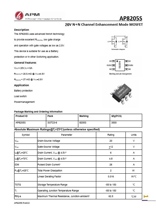
20V N +N Channel Enhancement Mode MOSFET1DescriptionThe AP8205S uses advanced trench technology to provide excellent R DS(ON), low gate charge and operation with gate voltages as low as 2.5V. This device is suitable for use as a Battery protection or in other Switching application.General FeaturesV DS = 20V, I D = 6AR DS(ON) < 20.5.mΩ @ V GS =4.5V R DS(ON) < 27.mΩ @ V GS =2.5VApplicationBattery protection Load switch PowermanagementPackage Marking and Ordering Information Absolute Maximum Ratings@T j =25o C(unless otherwise specified)8205S20V N+N Channel Enhancement Mode MOSFETo220V N +N Channel Enhancement Mode MOSFET3Fig 1. Typical Output Characteristics Fig 2. Typical Output CharacteristicsFig 3. On-Resistance v.s. Gate VoltageFig 4. Normalized On-Resistancev.s. TemperatureFig 5. Forward Characteristic ofFig 6. Gate Threshold Voltage v.s.Reverse DiodeJunction Temperature20V N +4Fig 7. Gate Charge Characteristics Fig 8. Typical Capacitance CharacteristicsFig 9. Maximum Safe Operating AreaFig 11. Transfer Characteristics Fig 12. Gate Charge Waveform20V N +N Channel Enhancement Mode MOSFET5SOT23-6PACKAGE INFORMATION20V N+N Channel Enhancement Mode MOSFETAttention1,Any and all APM Microelectronics products described or contained herein do not have specificationsthat can handle applications that require extremely high levels of reliability, such as life support systems, aircraft's control systems, or other applications whose failure can be reasonably expected to result in serious physical and/or material damage. Consult with your APM Microelectronics representative nearest you before using any APM Microelectronics products described or contained herein in such applications.2,APM Microelectronics assumes no responsibility for equipment failures that result from using productsat values that exceed, even momentarily, rated values (such as maximum ratings, operating condition ranges, or other parameters) listed in products specifications of any and all APM Microelectronicsproducts described or contained herein.3, Specifications of any and all APM Microelectronics products described or contained here instipulate the performance, characteristics, and functions of the described products in the independent state, and arenot guarantees of the performance, characteristics, and functions of the described products as mountedin the customer’s products or equipment. To verify symptoms and states that cannot be evaluated in an independent device, the customer should always evaluate and test devices mounted in the customer’s products or equipment.4, APM Microelectronics Semiconductor CO., LTD. strives to supply high quality high reliability products. However, any and all semiconductor products fail with some probability. It is possible that these probabilistic failures could give rise to accidents or events that could endanger human lives that couldgive rise to smoke or fire, or that could cause damage to other property. When designing equipment,adopt safety measures so that these kinds of accidents or events cannot occur. Such measures includebut are not limited to protective circuits and error prevention circuits for safe design, redundantdesign,and structural design.5,In the event that any or all APM Microelectronics products(including technical data, services) describedor contained herein are controlled under any of applicable local export control laws and regulations, such products must not be exported without obtaining the export license from the authorities concerned in accordance with the above law.6, No part of this publication may be reproduced or transmitted in any form or by any means,electronic or mechanical, including photocopying and recording, or any information storage or retrieval system, or otherwise, without the prior written permission of APM Microelectronics Semiconductor CO., LTD.7, Information (including circuit diagrams and circuit parameters) herein is for example only; it is not guaranteed for volume production. APM Microelectronics believes information herein is accurate and reliable, but no guarantees are made or implied regarding its use or any infringements of intellectual property rights or other rights of third parties.8, Any and all information described or contained herein are subject to change without notice due to product/technology improvement,etc. When designing equipment, refer to the "Delivery Specification" for the APM Microelectronics product that you Intend to use.6。
APM2306中文资料
VGS(th)-Threshold Voltage (V)
2.00
100 80 60
VGS=10V V GS=5V
1.75
1.50
40 20 0 0 2 4 6 8 10
1.25
1.00 -50
-25
0
25
50
75
100
125
150
Tj - Junction Temperatnt (A)
元器件交易网
APM2306
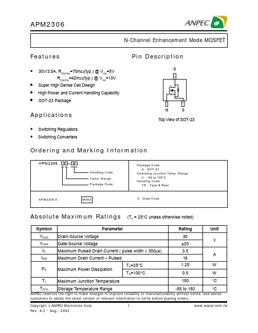
N-Channel Enhancement Mode MOSFET
Features
• • • •
30V/3.5A, RDS(ON)=70mΩ(typ.) @ VGS=5V RDS(ON)=42mΩ(typ.) @ VGS=10V Super High Dense Cell Design High Power and Current Handling Capability SOT-23 Package
4
元器件交易网
APM2306
Typical Characteristics
Source-Drain Diode Forward Voltage
30
Single Pulse Power
14 12
IS-Source Current (A)
Power (W)
120
On-Resistance vs. Junction Temperature
70
RDS(on)-On-Resistance (mΩ)
RDS(on)-On Resistance (mΩ)
V GS=10V ID=3.5A
100 80
ID=3.5A
2300场效应管参数
2300 场效应管(FET)是一种金属氧化物半导体场效应管(MOSFET),常用于放大、开关、调制、逻辑等电路。
其具体参数包括:
1. 漏极电流(Id):在栅源电压(Vgs)为0 时,漏极电流与栅极漏极电压(Vgd)之间的关系。
Id 随着Vgd 的增大而增大。
2. 阈值电压(Vth):栅源电压Vgs 大于阈值电压时,场效应管开始导通。
Vth 的大小影响器件的开关速度和功耗。
3. 饱和区电流(Isat):当栅源电压Vgs 足够大时,场效应管进入饱和区,Isat 表示饱和区内的电流值。
4. 输入阻抗(Zin):场效应管的输入阻抗较高,通常在10^9Ω以上,这意味着输入电流很小。
5. 输出阻抗(Zout):场效应管的输出阻抗较低,通常在几十欧姆至几百欧姆之间,取决于负载电阻。
6. 开关速度(ton,toff):场效应管从导通到截止,或从截止到导通所需的时间。
开关速度越快,功耗越低,但可能导致电磁干扰(EMI)问题。
7. 跨导(gm):表示场效应管在单位栅源电压下的电流增益。
跨导越大,放大能力越强。
8. 耗尽模式(Depletion-mode)或增强模式(Enhancement-mode):根据导电通道的极性,场效应管可分为耗尽模式和增强模式。
耗尽模式在场效应管开启时,栅极附近的导电通道被耗尽;增强模式在场效应管开启时,栅极附近的导电通道被增强。
AP30N06D 30A 60V TO-252
DescriptionThe AP30N06D uses advanced trench technologyto provide excellent R DS(ON), low gate charge andoperation with gate voltages as low as 4.5V. Thisdevice is suitable for use as aBattery protection or in other Switching application.General FeaturesV DS = 60V I D =30 AR DS(ON) < 30mΩ @ V GS=10VApplicationBattery protectionLoad switchUninterruptible power supplyPackage Marking and Ordering InformationProduct ID Pack Marking Qty(PCS)AP30N06D TO-252-3AP30N06D XXXX YYYY2500Absolute Maximum Ratings (T C=25℃unless otherwise noted)Symbol Parameter Rating UnitsV DS Drain-Source Voltage60 VV GS Gate-Sou r ce Voltage ±20VI D@T C=25℃Continuous Drain Current, V GS @ 10V130 AI D@T C=100℃Continuous Drain Current, V GS @ 10V115 AI D@T A=25℃Continuous Drain Current, V GS @ 10V1 5.6 AI D@T A=70℃Continuous Drain Current, V GS @ 10V1 4.5 AI DM Pulsed Drain Current246 AEAS Single Pulse Avalanche Energy325.5 mJI AS Avalanche Current 22.6 AP D@T C=25℃Total Power Dissipation434.7 WP D@T A=25℃Total Power Dissipation4 2 W T STG Storage Temperature Range -55 to 150 ℃T J Operating Junction Temperature Range -55 to 150 ℃1 AP30N06D R ve3.8 臺灣永源微電子科技有限公司AP30N06D R ve 3.8 臺灣永源微電子科技有限公司2R θJA Thermal Resistance Junction-Ambient 1 62 ℃/W R θJCThermal Resistance Junction-Case 13.6℃/WJ Symbol ParameterConditionsMin. Typ. Max. Unit BV DSSDrain-Source Breakdown VoltageV GS =0V , I D =250uA 60 --- --- V △BV DSS /△T J BV DSS Temperature CoefficientReference to 25℃ , I D =1mA --- 0.063 --- V/℃R DS(ON) Static Drain-Source On-Resistance 2V GS =10V , I D =15A--- 25 30 m Ω V GS =4.5V , I D =10A--- 30 38 V GS(th) Gate Threshold Voltage V GS =V DS , I D =250uA 1.2 --- 2.5 V △V GS(th) V GS(th) Temperature Coefficient --- -5.24 --- mV/℃ I DSS Drain-Source Leakage Current V DS =48V , V GS =0V , T J =25℃ --- --- 1 uA V DS =48V , V GS =0V , T J =55℃ --- --- 5 I GSS Gate-Source Leakage Current V GS =±20V , V DS =0V --- --- ±100 nA gfs Forward Transconductance V DS =5V , I D =15A --- 17 --- S R g Gate Resistance V DS =0V , V GS =0V , f=1MHz--- 3.2 --- Ω Q g Total Gate Charge (4.5V) V DS =48V , V GS =4.5V , I D =12A --- 12.6 --- nC Q gs Gate-Source Charge --- 3.2 --- Q gd Gate-Drain Charge --- 6.3 --- T d(on) Turn-On Delay Time V DD =30V , V GS =10V , R G =3.3, I D =10A--- 8 --- ns T r Rise Time --- 14.2 --- T d(off) Turn-Off Delay Time --- 24.4 --- T f Fall Time --- 4.6 --- C iss Input Capacitance V DS =15V , V GS =0V , f=1MHz --- 1378 --- pF C oss Output Capacitance --- 86 --- C rss Reverse Transfer Capacitance --- 64 --- I S Continuous Source Current 1,5 V G =V D =0V , Force Current --- --- 23 A I SM Pulsed Source Current 2,5 --- --- 46 A V SDDiode Forward Voltage 2V GS =0V , I S =1A , T J =25℃ ------1.2V Note :1.The data tested by surface mounted on a 1 inch2 FR-4 board with 2OZ copper.2.The data tested by pulsed , pulse width ≦ 300us , duty cycle ≦ 2%3.The EAS data shows Max. rating . The test condition is VDD=25V,VGS=10V,L=0.1mH,IAS=22.6A4.The power dissipation is limited by 150℃ junction temperature5.The data is theoretically the same as ID and IDM , in real applications , should be limited by total power dissipation.3150Typical Characteristics Fig.1 Typical Output Characteristics Fig.2 On-Resistance v.s Gate-SourceFig.5 Normalized V GS(th) v.s T JFig.3 Forward Characteristics of Reverse Fig.4 Gate-Charge Characteristics4I ASV GSBV DSS V DDEAS=12L x I AS 2 x BV DSSBV DSS -V DDFig.8 Safe Operating Area Fig.7 Capacitance Fig.10 Switching Time Waveform Fig.11 Unclamped Inductive Waveform5Package Mechanical DataDimensionsMillimeters Inches Ref.Min.Typ.Max.Min.Typ.Max.A A2B C D E G H LV1V22.1000.660.40 2.500.100.860.600.08300.0260.0160.0980.0040.0340.0246.409.5010.700.3740.4210.0530.0655.906.30L20°6°0.2320.2486.800.2520.2684.47 4.670.1760.1841.09 1.210.0430.0487°1.35 1.650°6°7°B2 5.18 5.480.2020.216C20.440.580.0170.023D1E15.30REF4.630.1820.209REFDETAIL ATO-252Reel Spectification-TO-252 ABBDimensionsMillimeters Inches Ref.Min.Typ.Max.Min.Typ.Max.W E F D0D1P0P1P2A0B0K0T t115.901.657.401.4016.101.857.601.600.6260.0650.2910.0550.6340.0730.2990.0631.40 1.607.9010.4510.600.4110.4170.240.270.0090.0110.0550.0633.90 4.106.900.27110P00.1540.1618.100.3110.3191.90 2.100.0750.0830.100.00440.001.5752.780.10916.001.757.501.501.504.008.002.0010.500.6300.0690.2950.0590.0590.1570.3150.0790.4136.857.002.68 2.880.2700.2760.1050.11339.8040.201.5671.583Attention1,Any and all APM Microelectronics products described or contained herein do not have specifications that can handle applications that require extremely high levels of reliability, such as life support systems, aircraft's control systems, or other applications whose failure can be reasonably expected to result in serious physical and/or material damage. Consult with your APM Microelectronics representative nearest you before using any APM Microelectronics products described or contained herein in such applications. 2,APM Microelectronics assumes no responsibility for equipment failures that result from using products at values that exceed, even momentarily, rated values (such as maximum ratings, operating condition ranges, or other parameters) listed in products specifications of any and all APM Microelectronics products described or contained herein.3, Specifications of any and all APM Microelectronics products described or contained here instipulate the performance, characteristics, and functions of the described products in the independent state, and are not guarantees of the performance, characteristics, and functions of the described products as mounted in the customer’s products or equipment. To verify symptoms and states that cannot be evaluated in an independent device, the customer should always evaluate and test devices mounted in the customer’s products or equipment.4, APM Microelectronics Semiconductor CO., LTD. strives to supply high quality high reliability products. However, any and all semiconductor products fail with some probability. It is possible that these probabilistic failures could give rise to accidents or events that could endanger human lives that could give rise to smoke or fire, or that could cause damage to other property. When designing equipment, adopt safety measures so that these kinds of accidents or events cannot occur. Such measures include but are not limited to protective circuits and error prevention circuits for safe design, redundantdesign,and structural design.5,In the event that any or all APM Microelectronics products(including technical data, services) described or contained herein are controlled under any of applicable local export control laws and regulations, such products must not be exported without obtaining the export license from the authorities concerned in accordance with the above law.6, No part of this publication may be reproduced or transmitted in any form or by any means,electronic or mechanical, including photocopying and recording, or any information storage or retrieval system, or otherwise, without the prior written permission of APM Microelectronics Semiconductor CO., LTD.7, Information (including circuit diagrams and circuit parameters) herein is for example only; it is not guaranteed for volume production. APM Microelectronics believes information herein is accurate and reliable, but no guarantees are made or implied regarding its use or any infringements of intellectual property rights or other rights of third parties.8, Any and all information described or contained herein are subject to change without notice due to product/technology improvement,etc. When designing equipment, refer to the "Delivery Specification" for the APM Microelectronics product that you Intend to use.6。
2301 MOS管
深圳市富满电子集团股份有限公司SHEN ZHEN FINE MAD ELECTRONICS GROUP CO.,LTD.2301(文件编号:S&CIC1241)18V P 沟道增强型MOS 场效应管VDS=-18VRDS(ON),Vgs@-4.5V,Ids@-1.0A =60mΩ@TYP RDS(ON),Vgs@-2.5V,Ids@-0.5A =82mΩ@TYP一、特点高级的加工技术极低的导通电阻高密度的单元设计SOT-23内部结构示意图二、最大额定值和热特性(T A =25℃,除非另有说明)参数符号值单位漏源电压V DS -18V栅源电压V GS ±12漏极电流I D -2.8A漏极脉冲电流I DM -6最大功耗T A =25℃P D 1.25W T A =75℃0.8工作结温和存储温度范围T J ,T stg -55to 150℃结环热阻(PCB 安装)R θJA140W/℃注:1、电流值取决于焊线的数量和线径。
2、重复性极限值:脉冲宽度由最高结温限制。
123321SourceDrain GateInternal Schemaic DiagramP-Channel MOSFET深圳市富满电子集团股份有限公司SHEN ZHEN FINE MAD ELECTRONICS GROUP CO.,LTD. 2301(文件编号:S&CIC1241)18V P沟道增强型MOS场效应管三、电特性参数符号测试条件最小典型最大单位静电漏源击穿电压BV DSS V GS=0V,I D=250uA-12-18--V漏源电阻R DS(on)V GS=-4.5V,I D=-1A--6085mΩR DS(on)V GS=-2.5V,I D=-0.5A--82115mΩ栅极阈值电压V GS(th)V DS=V GS,I D=250uA-0.4-0.7-1.1V 栅源短路时,漏极电流I DSS V DS=-12V,V GS=0V----1uA 漏极短路时截止栅电流I GSS V GS=±12V,I DS=0uA----±100nA 动态总栅极电荷Q gV DS=-6V,I D=-2.8AV GS=-4.5V ------nC栅源电荷Qg s------栅漏电荷Q gd------延迟时间(On)t d(on)V DD=-6V,R L=6ΩI D=-1A,V GEN=-4.5VR G=6Ω------ns上升时间(On)t r------延迟时间(Off)t d(off)------下降时间(Off)t f------输入电容C issV DS=-6V,V GS=0Vf=1.0MHz ------pF输出电容C oss------反向传输电容C rss------漏源二极管二极管最大正向电流I S------ 1.6A 二极管正向电压V SD I S=-1.6A,V GS=0V---0.75--V 注:脉冲测试:脉冲宽度<=300us,占空比<=2%。
AP2306AGN
N-CHANNEL ENHANCEMENT MODE POWER MOSFET▼ Capable of 2.5V gate drive BVDSS 30V ▼ Lower on-resistance R DS(ON)35m Ω▼ Surface mount packageI D5ADescriptionAbsolute Maximum RatingsSymbol Units V DS V V GSV I D @T A =25℃A I D @T A =70℃A I DMA P D @T A =25℃W W/℃T STG ℃T J℃Symbol Value Unit Rthj-aThermal Resistance Junction-ambient 3Max.90℃/WData and specifications subject to change without notice200105041AP2306AGNPb Free Plating ProductParameterRating Drain-Source Voltage 30Gate-Source VoltageContinuous Drain Current 3, V GS @ 4.5V 5Continuous Drain Current 3, V GS @ 4.5V 4Pulsed Drain Current 120Total Power Dissipation 1.38-55 to 150Operating Junction Temperature Range-55 to 150Linear Derating Factor 0.01Thermal DataParameterStorage Temperature Range± 12DGSSOT-23Advanced Power MOSFETs utilized advanced processing techniques to achieve the lowest possible on-resistance, extremely efficient and cost-effectiveness device.The SOT-23 package is universally used for all commercial-industrial applications.Electrical Characteristics@T j =25o C(unless otherwise specified)Symbol ParameterTest ConditionsMin.Typ.Max.Units BV DSSDrain-Source Breakdown VoltageV GS =0V, I D =250uA30--V ΔB V DSS /ΔT jBreakdown Voltage Temperature Coefficient Reference to 25℃, I D =1mA-0.1-V/℃R DS(ON)Static Drain-Source On-ResistanceV GS =10V, I D =5A --30m ΩV GS =4.5V, I D =5A --35m ΩV GS =2.5V, I D =2.6A --50m ΩV GS =1.8V, I D =1.0A--90m ΩV GS(th)Gate Threshold Voltage V DS =V GS , I D =250uA 0.5- 1.2V g fs Forward TransconductanceV DS =5V, I D =5A -13-S I DSS Drain-Source Leakage Current (T j =25o C)V DS =30V, V GS =0V --1uA Drain-Source Leakage Current (T j =70o C)V DS =24V ,V GS =0V --25uA I GSS Gate-Source Leakage V GS =--nA Q g Total Gate Charge 2I D =5A -8.515nC Q gs Gate-Source Charge V DS =16V - 1.5-nC Q gd Gate-Drain ("Miller") Charge V GS =4.5V - 3.2-nC t d(on)Turn-on Delay Time 2V DS =15V -6-ns t r Rise TimeI D =5A-20-ns t d(off)Turn-off Delay Time R G =3.3Ω,V GS =10V -20-ns t f Fall Time R D =3Ω-3-ns C iss Input Capacitance V GS =0V -6601050pF C oss Output CapacitanceV DS =25V -90-pF C rssReverse Transfer Capacitancef=1.0MHz-70-pFSource-Drain DiodeSymbol ParameterTest ConditionsMin.Typ.Max.Units V SD Forward On Voltage 2I S =1.2A, V GS =0V -- 1.2V t rr Reverse Recovery Time2I S =5A, V GS =0V,-14-ns Q rrReverse Recovery ChargedI/dt=100A/µs-7-nCNotes:1.Pulse width limited by Max. junction temperature.2.Pulse width <300us , duty cycle <2%.3.Surface mounted on 1 in 2 copper pad of FR4 board ; 270℃/W when mounted on min. copper pad.± 12V ±100AP2306AGNFig 1. Typical Output CharacteristicsFig 4. Normalized On-Resistancev.s. Junction TemperatureFig 5. Forward Characteristic ofFig 6. Gate Threshold Voltage v.s.Reverse DiodeJunction TemperatureFig 7. Gate Charge Characteristics Fig 8. Typical Capacitance CharacteristicsFig 9. Maximum Safe Operating Area Fig 10. Effective Transient Thermal ImpedanceFig 11. Switching Time Waveform Fig 12. Gate Charge WaveformAP2306AGN。
2302 mos 规格书
10 nC
pF
td(on) tr td(off) tf VDD=10V, RL=5.5Ω, ID ≈3.6A, VGEN=4.5V,Rg=6Ω
7 55 16 10
15 80 60 25 ns
Notes :
ٛ. ٛ.
Pulse Test : Pulse width≤300µs, duty cycle ≤2%. These parameters have no way to verify.
Electrical characteristics (Ta=25℃ unless otherwise noted)
Symbo l V(BR)DSS VGS(th) IGSS IDSS rDS(on) gfs VSD
Parameter Static Drain-source breakdown voltage Gate-threshold voltage Gate-body leakage Zero gate voltage drain current Drain-source on-resistancea Forward transconductancea Diode forward voltage Dynamic Total gate charge Gate-source charge Gate-drain charge Input capacitance b Output capacitance b Reverse transfer capacitanceb Switchingb Turn-on delay time Rise time Turn-off delay time Fall time
SHENZHEN CHANGHAO MICRO-ELECTRONICS CO.,LTD SOT-23 Plastic-Encapsulate MOSFETS
- 1、下载文档前请自行甄别文档内容的完整性,平台不提供额外的编辑、内容补充、找答案等附加服务。
- 2、"仅部分预览"的文档,不可在线预览部分如存在完整性等问题,可反馈申请退款(可完整预览的文档不适用该条件!)。
- 3、如文档侵犯您的权益,请联系客服反馈,我们会尽快为您处理(人工客服工作时间:9:00-18:30)。
SOT-23場效應晶體管(SOT-23Field Effect
Transistors)
P-Channel Enhancement-Mode MOS FETs P 沟道增强型MOS 场效应管
■MAXIMUM
RATINGS 最大額定值
Characteristic
特性參數
Symbol 符號Max 最大值Unit 單位Drain-Source V oltage 漏極-源極電壓BV DSS -30V Gate-Source Voltage 栅極-源極電壓
V GS +12V Drain Current (continuous)漏極電流-連續I D -4.2A Drain Current (pulsed)漏極電流-脉冲
I DM
-18
A
Total Device Dissipation 總耗散功率
T A =25℃環境溫度爲25℃P D 1400mW
Junction 結溫
T J 150℃Storage Temperature 儲存溫度
T stg
-55to+150
℃
AP2306AGN
■ELECTRICAL CHARACTERISTICS
電特性
(T A =25℃unless otherwise noted 如無特殊說明,溫度爲25℃
)
Characteristic
特性參數
Symbol 符號Min 最小值Typ 典型值Max 最大值Unit 單位Drain-Source Breakdown Voltage
漏極-源極擊穿電壓(I D =-250uA,V GS =0V)BV DSS -30——V Gate Threshold Voltage
栅極開启電壓(I D =-250uA,V GS =V DS )V GS(th)-0.6—-2V Diode Forward Voltage Drop
内附二極管正向壓降(I S =-1A,V GS =0V)V SD —
—
-1
V
Zero Gate Voltage Drain Current
零栅壓漏極電流(V GS =0V,V DS =-24V)(V GS =0V,V DS =-24V ,T A =55℃)I DSS ——
-1-5u A
Gate Body Leakage
栅極漏電流(V GS =+12V,V DS =0V)I GSS ——+100n A Static Drain-Source On-State Resistance 静态漏源導通電阻(I D =-4.2A,V GS =-10V)R DS(ON)—4250mΩ
Static Drain-Source On-State Resistance 静态漏源導通電阻(I D =-2A,V GS =-4.5V)R DS(ON)—5360mΩ
Static Drain-Source On-State Resistance 静态漏源導通電阻(I D =-1A,V GS =-2.5V)R DS(ON)—8085mΩ
Input Capacitance 輸入電容(V GS =0V,V DS =-15V,f=1MHz)C ISS —954—pF Output Capacitance 輸出電容(V GS =0V,V DS =-15V,f=1MHz)C OSS —115—pF Turn-ON Time 开启時間
(V DS =-15V,V GS =-10V,R GEN =6Ω)t (on)—6—ns Turn-OFF Time 关断時間
(V DS =-15V,V GS =-10V,R GEN =6Ω)t (off)
—
38
—
ns
Pulse Width<300μs;Duty Cycle<2.0%
AP2306AGN
■TYPICAL CHARACTERISTIC CURVE
典型特性曲线
Fig1:Output Characteristics Figure2:Transfer
Characteristics Figure3:On-Resistance vs.Drain Current and Gate Voltage Figure4:On-Resistance vs.Gate-Source
Voltage Figure5:Gate-Charge Characteristics Figure6:Safe Operating Area
AP2306AGN。