单片机扩展芯片8243的中文资料
STM8S103F2P6

4.10 TIM1 — 16位高级控制定时器............................................................................................11
4.11
TIM2 — 16位通用定时器...................................................................................................11
6 存储器和寄存器映像................................................................................................19
6.1
存储器映像 ........................................................................................................................19
21个高吸收电流输出 非常强健的I/O设计,对倒灌电流有非常
强的承受能力
开发支持 单线接口模块(SWIM)和调试模块(DM),
可以方便地进行在线编程和非侵入式调 试
本文档英文原文下载地址: /stonline/products/literature/ds/15441.pdf
参照2009年6月 STM8S103x 数据手册英文第3版 本译文仅供参考,如有翻译错误,请以英文原稿为准。请读者随时注意在ST网站下载更新版本
目录
STM8S103xx数据手册
目录
1 简介...........................................................................................................................4
P8242AH资料
Y
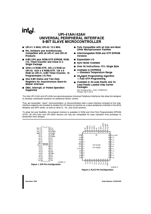
Fully Compatible with all Intel and Most Other Microprocessor Families Interchangeable ROM and OTP EPROM Versions Expandable I O Sync Mode Available Over 90 Instructions 70% Single Byte Available in EXPRESS Standard Temperature Range inteligent Programming Algorithm Fast OTP Programming Available in 40-Lead Plastic and 44Lead Plastic Leaded Chip Carrier Packages
Contact factory for current code revision available in all versions of the 8242 product lines
2
元器件交易网
UPI-41AH 42AH
Table 1 Pin Description
210393 – 2
Figure 1 DIP Pin Configuration
210393 – 3
Figure 2 PLCC Pin Configuration
November 1994
Order Number 210393-008
元器件交易网
UPI-41AH 42AH
Symbol DIP Pin No 1 39 PLCC Pin Type No 2 43 I Name and Function
TEST 0 TEST 1
0832芯片

w
w
w
A0 ~ A9
地 port1 址 译 port2 码
f
p
.
CS
VREF
-5V
-10V
10V
XFER DGND
例2
利用上例连线图,编程输出一锯齿波.
Vo 4V
w
0V
.
f
p
g
a -
a
r m
w
w
t
21
w
start: MOV MOV next: MOV OUT MOV OUT CALL INC CMP JNZ MOV LOOP
.
2)双缓冲工作方式
f
p
g
a -
1)单缓冲工作方式
a
8
r m
一个工作于受控锁存器状态
在不要求多相D/A同时输出时,可以采用单缓冲方式,
w
w
可以提高D/A的数据吞吐量.
w
此时只需一次写操作,就开始转换,
.
f
p
g
a -
一个寄存器工作于直通状态,
a
9
r m
1)单缓冲工作方式 :
a -
a
D0 ~ D7 +5V IOW A0 ~ A9
CX, 8000H AL, 0 DX, port1 DX, AL DX, port2 DX, AL delay AL AL, 0CEH next AL, 0 next
a -
4V 0V
;锯齿谷值 ;打开第一级锁存 ;打开第二级锁存
a
Vo
;波形个数
MOV AH, 4CH INT 21H ;子程delay (略) code ENDS END start
CXP82432A资料

DescriptionThe CXP82432A/82440A is a CMOS 8-bit single chip microcomputer integrating on a single chip an A/D converter, serial interface, timer/counter, time base timer, capture timer counter, fluorescent display tube controller/driver, remote control reception circuit,CTL duty detection circuit, 14-bit PWM output and high-speed output circuit besides the basic configurations of 8-bit CPU, ROM, RAM, and I/O port.The CXP82432A/82440A also provides sleep/stop function that enables lower power consumption.Features•Wide-range instruction system (213 instructions) to cover various types of data —16-bit arithmetic/multiplication and division/boolean bit operation instructions •Minimum instruction cycle 400ns at 10MHz operation(122µs at 32kHz operation)•Incorporated ROM capacity 32K bytes (CXP82432A)40K bytes (CXP82440A)•Incorporated RAM capacity 1120 bytes (including fluorescent display area)•Peripheral functions — A/D converter 8-bit, 8-channel, successive approximation method(Conversion time of 32µs/10MHz)— Serial interface 8-bit, 8-stage FIFO incorporated(Auto transfer for 1 to 8 bytes), 1 channel 8-bit clock synchronized type, 1 channel— Timers 8-bit timer, 8-bit timer/counter, 19-bit time base timer16-bit capture timer/counter, 32kHz timer/counter— Fluorescent display tube controller/driver Maximum of 384 segments display possible1 to 16-digit dynamic display Dimmer functionHigh voltage drive output (40V)Incorporated pull-down resistor (Mask option)Hardware key scan functionMaximum of 16 x 8 key matrix compatible— Remote control reception circuit Incorporated noise elimination circuit8-bit pulse measuring counter, 6-stage FIFO— PWM output circuit 14 bits, 1 channel — CTL duty detection circuit — High-speed output circuit Precision of 800ns at 10MHz, 4 outputs •Interruption 19 factors, 15 vectors, multi-interruption possible •Standby mode SLEEP/STOP •Package 100-pin plastic QFP •Piggyback/evaluation chip CXP82400A 100-pin ceramic QFP– 1–CXP82432A/82440AE94Z15-PPCMOS 8-bit Single Chip MicrocomputerSony reserves the right to change products and specifications without prior notice. This information does not convey any license byany implication or otherwise under any patents or other right. Application circuits shown, if any, are typical examples illustrating the operation of the devices. Sony cannot assume responsibility for any problems arising out of the use of these circuits.StructureSilicon gate CMOS IC– 2–CXP82432A/82440AB l o c k D i a g r a mP E 2/I N T 2P E 3/I N T 3/N M IP A 0/A N 0 t o P A 7/A N 7A 0 t o P A 7R S TV D D V S S B 0 t o P B 6C 0 t o P C 7D 0 t o P D 7E 0 t o P E 5F 0 t o P F 7G 0 t o P G 7H 0 t o P H 7E 6 t o P E 7T E X E X T A L X T A L T X A V R E FA V S ST 0 t o T 7T 15/S 24 t o T 8/S 31P D 0/S 0 t o P I 7/S 23V F D PP E 5/C T L P E 4/R M C P B 3/S I 0P B 4/S O 0P B 6/S I 1P B 7/S O 1P B 5/S C K 1P E 0/I N T 0/E C 0P E 7/T O P B 0/C I N T P E 1/I N T 2/E C 1P B 1/C S 0P B 2/S C K 0B 7I 0 t o P I 7P G 0/R T O 0 t o P G 3/R T O 3P E 0/E C 0/I N T 0P E 1/E C 1/I N T 1P E 6/P W MP E 7/D D OP E 7/A D JCXP82432A/82440A Pin Assignment(Top View)PE1/EC1/INT1PE2/INT2 PE3/INT3/NMIPE4/RMCPE5/CTLPE6/PWM PE7/TO/DDO/ADJPB0/CINTPB1/CS0PB2/SCK0PB3/SI0PB4/SO0PB5/SCK1PB6/SI1PB7/SO1PC0/KR0PC1/KR1PC2/KR2PC3/KR3PC4/KR4PC5/KR5PC6/KR6PC7/KR7PH0PH1PH2PH3PH4PH5PH6T7T8/S31T9/S30T10/S29T11/S28T12/S27T13/S26T14/S25T15/S24PI7/S23PI6/S22PI5/S21PI4/S20PI3/S19PI2/S18PI1/S17PI0/S16PF7/S15PF6/S14PF5/S13PF4/S12PF3/S11PF2/S10PF1/S9PF0/S8PD7/S7PD6/S6PD5/S5PD4/S4PD3/S3 PH7PA/ANPA1/AN1PA2/AN2PA3/AN3PA4/AN4PA5/AN5RSTEXTALXTALVssTXTEXPA6/AN6PA7/AN7AVREFAVssPD/SPD1/S1PD2/S2 PE/EC/INTPG7PG6PG5PG4PG3/RTO3PG2/RTO2PG1/RTO1PG/RTOVssNCVDDVFDPTT1T2T3T4T5T6Note) 1.NC (Pin 90) must be connected to V DD.2.Vss (Pins 41 and 91) must be connected to GND.– 3–– 4–CXP82432A/82440APin DescriptionPin code I/OFunctionsI/O/Analog inputPA0/AN0to PA7/AN7(Port A)8-bit I/O port. I/O can be set in single bit units.(8pins)Analog inputs to A/D converter. (8 pins)I/O/InputPC0/KR0to PC7/KR7PE0/INT0/EC0PE1/INT1/EC1PE2/INT2PE3/INT3/NMI PE4/RMC PE5/CTL PE6/PWM PE7/TO/DDO/ADJ PF0/S8to PF7/S15PG0/RTO0toPG3/RTO3PG4 to PG7Input/Input/Input Input/Input/Input Input/Input Input/Input/Input Input/Input Input/Input Output/Output Output/Output/Output/OutputOutput/OutputI/O/OutputI/O(Port C)8-bit I/O port. I/O canbe set in a unit of singlebits. Capable of driving 12mA sync current.Serves as key return inputs when operatingkey scan with FDP segment signal.Output/OutputPD0/S0to PD7/S7(Port D)8-bit output port. (8 pins)FDP segment signal outputs.(Port E)8-bit port. Lower 6 bits are for inputs; upper 2 bits are for outputs.(8 pins)(Port F)8-bit output port.(8pins)(Port G)8-bit I/O port. I/O can be set in a unit of single bits. Data for the lower 4 bits are gated with thecontents of RTO or OR-gate output. (8 pins)External event inputs for timer/counter.(2 pins)Inputs for external interruption request.(4 pins)Non-maskable interruption request input.Remote control reception circuit input.Input for CTL duty direction circuit.14-bit PWM output.Output for the 16-bit timer/counter rectangular waves, CTU duty detection, and 32kHz oscillation frequency demultiplication.FDP segment signal outputs.Outputs for real-time pulse generator (RTG).Functions as high-precision, real-time pulse output port.(4 pins)I/O/Input I/O/Input I/O/I/O I/O/Input I/O/Output I/O/I/O I/O/Input Output/OutputPB0/CINT PB1/CS0PB2/SCK0PB3/SI0PB4/SO0PB5/SCK1PB6/SI1PB7/SO1(Port B)8-bit I/O port. I/O for lower 7 bits can be set in a unit of single bits.Uppermost bit (PB7) is for output only.(8 pins)Capture input to 16-bit timer/counter.Chip select input for serial interface (CH0).Serial clock I/O (CH0).Serial data input (CH0).Serial data output (CH0).Serial clock I/O (CH1).Serial data input (CH1).Serial data output (CH1).– 5–CXP82432A/82440APin code I/O FunctionsOutput/OutputPI0/S16to PI7/S23(Port I)8-bit output ports.(8 pins)FDP segment signal outputs.Output/Output T8/S31to T15/S24Outputs for FDP timing (digit) signals/segment signals.I/OPH0 to PH7(Port H)8-bit I/O port. I/O can be set in a unit of single bits.(8 pins)V FDP EXTAL XTAL TEX TX RST NC AV REF AV SS V DD V SSInput Output Input Output InputInput FDP voltage supply when incorporated resistor is set by mask option.T0 to T7FDP timing signal outputs.Crystal connectors system clock oscillation. When the clock is supplied externally, input to EXTAL; opposite phase clock should be input to XTAL.Crystal connectors for 32kHz timer/counter clock oscillation. Set 32kHz crystal oscillator between TEX and TX. For usage as event input, attach clock source to TEX, and open TX.Low-level active, system reset.NC. Under normal operation, connect to V DD .Reference voltage input for A/D converter.A/D converter GND.Vcc supply.GND.OutputCXP82432A/82440A I/O Circuit Format for Pins– 6–CXP82432A/82440A– 7–CXP82432A/82440A– 8–CXP82432A/82440A– 9–– 10–CXP82432A/82440A∗1)V IN and V OUT must not exceed V DD + 0.3V.∗2)Specifies output current of general-purpose I/O ports.∗3)The high current drive transistor is the N-CH transistor of Port C (PC).Note)Usage exceeding absolute maximum ratings may permanently impair the LSI. Normal operation should beconducted under the recommended operating conditions. Exceeding these conditions may adversely affect the reliability of the LSI.Supply voltage Input voltage Output voltage Display output voltageHigh level output currentHigh level total output currentLow level output currentLow level total output current Operating temperature Storage temperatureAllowable power dissipation V DD AVss V IN V OUT V OD I OHI ODH1I ODH2∑I OH ∑I ODH I OL I OLC∑I OL Topr TstgP D–0.3 to +7.0–0.3 to +0.3–0.3 to +7.0∗1–0.3 to +7.0∗1V DD –40 to V DD +0.3–5–15–35–40–1001520100–20 to +75–55 to +150600V V V V V mA mA mA mA mA mA mA mA °C °C mWAs P channel transistor is open drain, V DD is reference.All pins excluding outputs ∗2(value per pin)Display outputs S0 to S23 (value per pin)Display outputs T0 to T7, and T8/S31 to T15/S24 (value per pin)Total for all pins excluding display outputs Total for all display outputs Port 1High current Port 1∗3Total for all output pinsItemSymbol Rating Unit RemarksAbsolute Maximum Ratings(Vss = 0V reference)High level input voltageLow level input voltageOperating temperatureSupply voltage 5.55.55.55.5V DD V DDV DD + 0.30.3V DD 0.2V DD 0.4+75V V V V V V V V V V °CItemSymbolMin.Max.Unit Remarks4.53.52.72.50.7V DD 0.8V DDV DD – 0.400–0.3–20V IHV IHS V IHEX V ILV ILS V ILEX ToprHigh-speed modeGuaranteed operation range Low-speed modeGuaranteed operation rangeGuaranteed operation range with TEX clockGuaranteed data hold range during STOP ∗1Hysteresis input ∗2EXTAL ∗3∗1Hysteresis input ∗2EXTAL ∗3V DD∗1)Value for each pin of normal input port (PA, PB4, PC, PG, PH).∗2)Value of the following pins: RST, CINT, CS0, SCK0, SCK1, SI0, SI1, EC0/INT0, EC1/INT1, INT2,INT3/NMI, RMC, CTL.∗3)Specifies only during external clock input.Recommended Operating Conditions(Vss = 0V reference)V DD = 4.5V, I OH = –0.5mA V DD = 4.5V, I OH = –1.2mA V DD = 4.5V, I OL = 1.8mA V DD = 4.5V, I OL = 3.6mA V DD = 4.5V, I OL = 12.0mA V DD = 5.5V, V IH = 5.5V V DD = 5.5V, V IL = 0.4V V DD = 5.5V, V IH = 5.5V V DD = 5.5V V IL = 0.4VV DD = 4.5VV OH = V DD – 2.5VV DD = 5.5VV OL = V DD – 35V V FDP = V DD – 35V V DD = 5VV FDP = V DD – 35VV DD = 5.5VV I = 0, 5.5VHigh level output current Display output current4.03.50.5–0.50.1–0.1–1.5–8–2060V V V V V µA µA µA µA µA mA mAµAk ΩµAPCPA, PB,PC, PE6,PE7, PG,PH EXTAL TEX RST ∗1Item Symbol Pins ConditionsMin.S0 to S23S24/T15 to S31/T8T0 to T7S0 to S23S24/T15 to S31/T8T0 to T7S0 to S23S24/T15 to S31/T8T0 to T7PA to PCPE, PG, PH,RST ∗1I OHOpen drain output leakage current(P-CH Tr off state)I LOLPull-down resistance ∗2I/Oleakage currentR L I IZV OHV OLI IHE I ILEI IHT I ILT I ILRLow leveloutput currentInput current100Typ.0.40.61.540–4010–10–400–20270±10Max.Unit DC CharacteristicsElectrical Characteristics (Ta = –20 to +75°C, Vss = 0V reference)∗1)RST specifies the input current when pull-up resistance has been selected; leakage current when noresistance has been selected. PB7 does not specify the leakage current because it’s only for output.∗2)When incorporated pull-down resistance has been selected through mask option.∗3)When all pins are open.Item Symbol Pins ConditionsMin.Typ.Max.UnitPower supply current ∗3Input capacityV DDPins other thanS0 to S31, T0 to T7,PB7, PE6,AV REF ,AV SS , V FDP ,V DD , V SSI DD1High speed mode operation(1/2 frequency demultiplier clock)I DDS1I DDS2I DDS3I DD2V DD = 5.5V, 10MHz crystal oscillation (C 1= C 2= 15pF)V DD = 3V, 32kHz crystal oscillation (C 1= C 2= 47pF)SLEEP modeSTOP modeV DD = 5.5V, 10MHz crystal oscillation;and termination of 32kHz oscillationV DD = 5.5V, 10MHz crystal oscillation (C 1= C 2= 15pF)V DD = 3V, 32kHz crystal oscillation (C 1= C 2= 47pF)2040mA35100µA1.28mA930µA 10µAC INClock 1MHz0V for all pins excluding measured pins1020pF∗t sys indicates the three values below according to the upper two bits (CPU clock selection) of the control clock registor (address: 00FE H ).tsys (ns)=2000/fc (upper two bits="00"), 4000/fc (upper two bits="01"), 16000/fc (upper two bits="11")Crystal oscillation Ceramic oscillationExternal clock32kHz clock application condition Crystal oscillationTEX EC0EC1EH EL EF ER t THt TLt TFt TRAC Characteristics (1) Clock timingSystem clock frequency System clock input pulse width System clock input rise time,fall timeEvent count input clock pulse widthEvent count input clock rise time, fall time System clock frequency Event count input pulse widthEvent count input rise time, fall timef Ct XL t XH t CR t CF t EH t EL t ER t EFf Ct TL t TH t TR t TFXTAL EXTAL EXTAL EXTAL EC0, EC1EC0, EC1TEX TX TEX TEXMHz ns ns nsmskHzµs msItemSymbol Pin Conditions Min.Unit Fig. 1, Fig. 2Fig. 1, Fig. 2External clock drive Fig. 1, Fig. 2External clock drive Fig. 3Fig. 3V DD = 2.7 to 5.5V Fig. 2 (32kHz clock application condition)Fig. 3Fig. 3137.5t sys + 50∗10Typ.32.768Max.102002020(Ta = –20 to +75°C, V DD = 4.5 to 5.5V, Vss = 0V reference)Fig. 3. Event count clock timingChip select transfer mode (SCK0 = output mode)Chip select transfer mode (SCK0 = output mode)Chip select transfer mode Chip select transfer mode Chip select transfer mode Note 1)t sys indicates the three values below according to the upper two bits (CPU clock selection) of thecontrol clock registor (address: 00FE H ).t sys (ns)=2000/fc (upper two bits="00"), 4000/fc (upper two bits="01"), 16000/fc (upper two bits="11")Note 2)The load condition for the SCK0 output mode, SO0 output delay time is 50pF + 1TTL.(2) Serial transfer (CH0)(Ta = –20 to +75°C, V DD = 4.5 to 5.5V, Vss = 0V reference)ItemCS0 ↓ →SCK0 delay time CS0 ↑ →SCK0 float delay time CS0 ↓ →SO0 delay time CS0 ↑ →SO0 float delay time CS0 High level width SCK0 cycle time SCK0High, Low level width SI0 input set-up time (for SCK0 ↑)SI0 input hold time (for SCK0 ↑)SCK0 ↓ →SO0delay timet DCSK t DCSKF t DCSOt DCSOF t WHCS t KCY t KH t KL t SIK t KSI t KSOSCK0SCK0SO0SO0CS0SCK0SCK0SI0SI0SO0Input mode Output mode Input mode Output mode SCK0 input mode SCK0 output mode SCK0 input mode SCK0 output mode SCK0 input mode SCK0 output modens ns ns ns ns SymbolPin Min.t sys + 200t sys + 200t sys + 200t sys + 200t sys + 2002t sys + 20016000/fct sys + 1008000/fc–50100200t sys + 200100ns ns ns ns ns ns ns nsns nst sys + 200100Max.Unit ConditionFig. 4. Serial transfer CH0 timingSCK0SI0SO0Serial transfer (CH1)(Ta = –20 to +75°C, V DD = 4.5 to 5.5V, Vss = 0V reference)ItemSCK1 cycle time t KCY SCK1Input mode Ouput mode Input mode Ouput mode SCK1 input mode SCK1 ouput mode SCK1 input mode SCK1 ouput mode SCK1 input mode SCK1 ouput mode100016000/fc 4008000/fc–50100200200100200100ns ns ns ns ns ns ns ns ns nsSCK1SI1SI1SO1t KH t KL t SIK t KSI t KSOSCK1High, Low level width SI1 input set-up time (for SCK1↑)SI1 input hold time (for SCK1↑)SCK1 ↓ →SO1 delay timeSymbolPin Condition Min.Max.Unit Note)The load condition for the SCK1output mode, SO1 output delay time is 50pF + 1TTL.Fig. 5. Serial transfer CH1 timingSO1SI1Conversion time Sampling time Reference input voltage Analog input voltaget CONV t SAMPV REF V IAN V ZT ∗1V FT ∗2I REFAV REFAN0 to AN7Ta = 25°C V DD = 5.0VV SS = AV SS = 0VOperation modeSLEEP mode STOP mode32kHz operation modeLinearity error Zero transition voltageFull-scaletransition voltage Resolution AV REF currentAV REFI REFSµs µsV V V DD AV REF 1.0mA 10µA0.6160/f ADC ∗312/f ADC ∗3V DD – 0.5ItemSymbol Pin Condition Min.Typ.Max.Unit Bits (3)A/D converter characteristics(Ta = –20 to +75°C, V DD = 4.5 to 5.5V, AV REF = 4.0 to AV DD , Vss = AV SS = 0V reference)8±3LSB 70mV 5030104970–104910mV Fig. 6. Definition of A/D converter termsAnalog inputV FTV ZT00H01H FE HFF H D i g i t a l c o n v e r s i o n v a l u e∗1)V ZT :Value at which the digital transfer value changesfrom 00H to 01H and vice versa.∗2)V FT :Value at which the digital transfer value changesfrom FE H to FF H and vice versa.∗3)f ADC indicates the below values due to ADC operationclock selection (ADCS: Bit 6 of address 00F9H ).During PS2 selection, f ADC = fc/2During PS1 selection, f ADC = fcExternal interruption High, Low level width Reset input Low level widthINT0INT1INT2NMI/INT3RST132/fc µsµsItemSymbolPin ConditionMin.Max.Unit t IH t IL t RSL(4) Interruption, reset input(Ta = –20 to +75°C, V DD = 4.5 to 5.5V, Vss = 0V reference)INT0INT1INT2falling edge)Fig. 7. Interruption input timingRSTFig. 8. RST input timing(5) Others(Ta = –20 to +75°C, V DD= 4.5 to 5.5V, Vss = 0V reference)ItemCLK inputHigh, Low level widtht CTH t CTLCTLt sys = 2000/fc t sys + 200nsSymbolPin ConditionMin.Max.Unit Fig. 9. Other timingCTLAppendixFig. 10. Recommended oscillation circuit(i) Main clock(ii) Main clock(iii) Sub clockManufacturer MURATA MFGCO., LTD.RIVER ELETEC CO., LTDKINSEKI LTD.Model CSA4.19MG CSA8.00MTZCST4.19MGW ∗CST8.00MTW ∗HC-49/U03HC-49/U (-S)P3fc (MHz)4.198.0010.004.198.0010.004.198.0010.004.198.0010.00202032.768kHz50223012273012270C 1(pF)C 2(pF)Rd (Ω)Circuitexample(i)CSA10.0MTZ (ii)CST10.0MTW ∗(i)1M (iii)Those marked with an asterisk (∗) signify types with built-in ground capacitance (C 1, C 2).ItemContentReset pin pull-up resistanceNon-existent Existent Non-existentExistentMask option tableHigh voltage drive output port pull-down resistance– 21–CXP82432A/82440APackage Outline Unit: mmSONY CODE EIAJ CODE JEDEC CODEPACKAGE MATERIALLEAD TREATMENT LEAD MATERIAL PACKAGE WEIGHTEPOXY RESIN SOLDER PLATING COPPER / 42 ALLOYPACKAGE STRUCTUREQFP-100P-L01100PIN QFP (PLASTIC)+ 0.1∗QFP100-P-1420-A1.4g元器件交易网。
S-8243BAEFT资料

S-8243BADFT S-8243BAEFT S-8243BAFFT
Note. Change in the detection voltage is available in products other than listed above. Contact the SII sales office.
S-8243B series
VDD
Rev. 1.0
Battery protection
VREG
DOP,COP RVCM,RVSM control
DOP
Voltage regulator
COP
Delay Delay Delay
660 kΩ
200nA
CTL1
VREG 1.4MΩ
Delay440 k ΩFra bibliotekCTL2
S-8243AACFT S-8243AADFT
Note. Change in the detection voltage is available in products other than listed above. Contact the SII sales office.
Table.2 S-8243B Series ( 4-serial cell )
(3) (4) (5) (6) (7) (8) (9)
(10) Low current consumption
Applications
• • Lithium-ion rechargeable battery packs Lithium- polymer rechargeable battery packs
(Overdischarge release voltage n (=Overdischarge detection voltage n + Hysteresis voltage n) can be selected within the range 2.0 V to 3.4 V.) (2) Three-level overcurrent protection including protection for short-circuiting • Overcurrent detection voltage 1 0.05 V to 0.3 V (50 mV step) Accuracy ±25 mV • Overcurrent detection voltage 2 0.5 V Accuracy ±100 mV • Overcurrent detection voltage 3 Accuracy ± 15 % VDD/2 Delay times for overcharge detection, overdischarge detection and overcurrent detection 1 can be set by external capacitors. (Delay times for overcurrent detection 2 and 3 are fixed internally.) Charge/discharge operation can be controlled through the control pins. High-accuracy battery monitor amp Voltage regulator High input-voltage device Wide operating voltage range Wide operating temperature range: Operation mode Power down mode (11) Small package GAMP = VBATTERY × 0.2 ± 1.0% VOUT = 3.3 V ± 2.4% (3 mA max.) Absolute maximum rating: 26 V 6 V to 18 V −40°C to +85 °C 120 µA max. 0.1 µA max. 16-Pin TSSOP package
ADC0832CCN
±1 ±1
± 1⁄2 ±1 ± 1⁄2 ±1
Molded (N) Molded (N) SO(M) PCC (V) PCC (V) Molded (N) C0831/ADC0832/ADC0834/ADC0838
Absolute Maximum Ratings
+
15 mA 6.5V
Operating Ratings (Notes 1, 2)
Supply Voltage, VCC Temperature Range ADC0832/8CIWM ADC0834BCN, ADC0838BCV, ADC0831/2/4/8CCN, ADC0838CCV, ADC0831/2/4/8CCWM 0˚C to +70˚C 4.5 VDC to 6.3 VDC TMIN≤TA≤TMAX −40˚C to +85˚C
2)
(Notes 1,
Dual-In-Line Package (Plastic) Molded Chip Carrier Package Vapor Phase (60 sec.) Infrared (15 sec.) ESD Susceptibility (Note 5)
260˚C 215˚C 220˚C 2000V
Key Specifications
n n n n n Resolution Total Unadjusted Error Single Supply Low Power Conversion Time 8 Bits
± 1⁄2 LSB and ± 1 LSB
5 VDC 15 mW 32 µs
Features
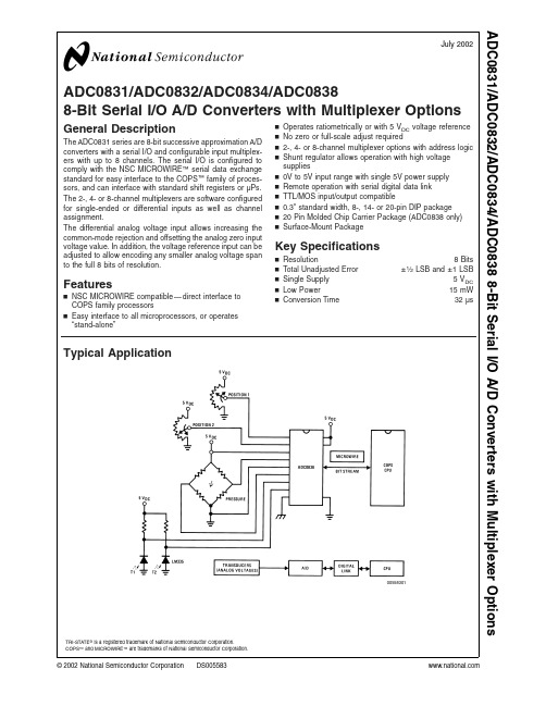
General Description
The ADC0831 series are 8-bit successive approximation A/D converters with a serial I/O and configurable input multiplexers with up to 8 channels. The serial I/O is configured to comply with the NSC MICROWIRE™ serial data exchange standard for easy interface to the COPS™ family of processors, and can interface with standard shift registers or µPs. The 2-, 4- or 8-channel multiplexers are software configured for single-ended or differential inputs as well as channel assignment. The differential analog voltage input allows increasing the common-mode rejection and offsetting the analog zero input voltage value. In addition, the voltage reference input can be adjusted to allow encoding any smaller analog voltage span to the full 8 bits of resolution. n n n n n n n n n n Operates ratiometrically or with 5 VDC voltage reference No zero or full-scale adjust required 2-, 4- or 8-channel multiplexer options with address logic Shunt regulator allows operation with high voltage supplies 0V to 5V input range with single 5V power supply Remote operation with serial digital data link TTL/MOS input/output compatible 0.3" standard width, 8-, 14- or 20-pin DIP package 20 Pin Molded Chip Carrier Package (ADC0838 only) Surface-Mount Package
FPGA可编程逻辑器件芯片EP4CE55F23C8N中文规格书

Four-Multiplier AdderIn the four-multiplier adder configuration shown in Figure 4–16, the DSP block canimplement 2 four-multiplier adders (1 four-multiplier adder per half-DSP block).These modes are useful for implementing one-dimensional and two-dimensionalfiltering applications. The four-multiplier adder is performed in two addition stages.The outputs of two of the four multipliers are initially summed in the two first-stageadder blocks. The results of these two adder blocks are then summed in thesecond-stage adder block to produce the final four-multiplier adder result, as shownin Equation 4–2 on page 4–4 and Equation 4–3 on page 4–5.Four-multiplier adder mode supports the rounding and saturation logic unit. You canuse the pipeline registers and output registers within the DSP block to pipeline themultiplier-adder result, increasing the performance of the DSP block.Figure 4–16.Four-Multiplier Adder Mode Shown for Half-DSP BlockNote to Figure 4–16:(1)Block output for accumulator overflow and saturate overflow.clock[3..0]ena[3..0]aclr[3..0]signasign bo u tp u t_ro u ndo u tp u t_sat u rateo v erflo w (1)I n p u t R e g i s t e r B a n k P i p e l i n e R e g i s t e r B a n k R o u n d /S a t u r a t e O u t p u t R e g i s t e r B a n kdataa_0[ ]data b _0[ ]dataa_1[ ]data b _1[ ]dataa_2[ ]data b _2[ ]dataa_3[ ]data b _3[ ]Half-DSP Block+++res u lt[ ]Figure4–8.12-Bit Independent Multiplier Mode Shown for Half-DSP BlockSoftware Support for Arria II Devices Software Support for Arria II DevicesAltera provides two distinct methods for implementing various modes of the DSPblock in a design: instantiation and inference. Both methods use the followingQuartus II megafunctions:■LPM_MULT ■ALTMULT_ADD ■ALTMULT_ACCUM ■ALTFP_MULTYou can instantiate the megafunctions in the Quartus II software to use the DSP block.Alternatively, with inference, you can create an HDL design and synthesize it with athird-party synthesis tool (such as LeonardoSpectrum, Synplify, or Quartus II NativeSynthesis) that infers the appropriate megafunction by recognizing multipliers,multiplier adders, multiplier accumulators, and shift functions. With either method,the Quartus II software maps the functionality to the DSP blocks during compilation.f For instructions about using the megafunctions and the MegaWizard Plug-InManager, refer to the Quartus II Software Help.f For more information, refer to Section III: Synthesis in volume 1 of the Quartus IIHandbook .shift_right shift_right = 1, shift right feature is enabled 1DSP Block Dynamic Signals per Full-DSP Blockclock0clock1clock2clock3DSP-block-wide clock signals 4ena0ena1ena2ena3Input and Pipeline Register enable signals 4aclr0aclr1aclr2aclr3DSP block-wide asynchronous clear signals (active low)4Total Count per Half- and Full-DSP Blocks 33Table 4–9.DSP Block Dynamic Signals for DSP Block in Arria II Devices (Part 2 of 2)Signal NameFunction Count。
单片机扩展芯片8243的中文资料
80C196单片机并行I/O端口扩展的方法汪建孙开放摘要:当用80C196单片机构成实际应用系统时,许多情况下需要扩展输入/输出端口。
本文介绍了用8243等芯片扩展该型单片机I/O端口的方法,从硬件连接和软件设计两个方面详细讨论了进行这种扩展的接口技术。
关键词:单片微机并行I/O 系统扩展1 引言80C196芯片是16位MCS-96系列单片机的重要成员,在工程应用领域有着广泛的应用[1]。
80C196KB/KC单片机共有5个8位的并行I/O端口:P0、P1、P2、P3和P4口。
虽然看起来I/O端口较多,但P0口同时用作片内A/D转换器的输入引脚ACH.0~ACH.7;P2口是多功能口,其中P2.0~P2.5共6个脚,具有复用功能,与芯片的其它功能共享;P3口和P4口一般用作系统总线AD0~AD15,通常不能再用作I/O口,这样当构成单片机应用系统后,只剩下P1口能作一般的I/O口使用,这对于稍大、稍复杂的系统而言,难以满足应用上的需求,实际中常需进行I/O口的扩展。
在单片机外部扩展I/O口时,可使用8155和8255等芯片[2, 3, 4]。
除此之外,还可用其它的集成电路芯片进行扩展。
本文从硬件连接和软件设计两个方面详细讨论了8243等多种芯片用于扩展80C196单片机系统并行I/O端口的方法。
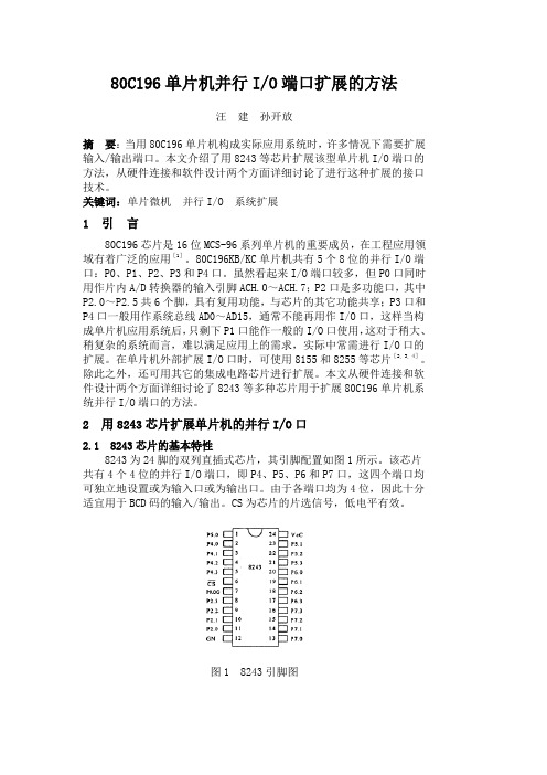
2 用8243芯片扩展单片机的并行I/O口2.1 8243芯片的基本特性8243为24脚的双列直插式芯片,其引脚配置如图1所示。
该芯片共有4个4位的并行I/O端口,即P4、P5、P6和P7口,这四个端口均可独立地设置或为输入口或为输出口。
由于各端口均为4位,因此十分适宜用于BCD码的输入/输出。
CS为芯片的片选信号,低电平有效。
图1 8243引脚图8243芯片的P2口(P2.0~P2.3)为控制及信号端口,其有两个作用,一是传送设置芯片各端口工作方式的命令及端口地址,二是传送经芯片输入/输出的数据。
在第一种情况下,由P2.1、P2.0指定端口的地址,由P2.3、P2.2规定端口的工作方式,各位具体的定义见表1。
- 1、下载文档前请自行甄别文档内容的完整性,平台不提供额外的编辑、内容补充、找答案等附加服务。
- 2、"仅部分预览"的文档,不可在线预览部分如存在完整性等问题,可反馈申请退款(可完整预览的文档不适用该条件!)。
- 3、如文档侵犯您的权益,请联系客服反馈,我们会尽快为您处理(人工客服工作时间:9:00-18:30)。
单片机扩展芯片8243的中文资料单片机扩展芯片8243中文资料。
引言。
单片机扩展芯片8243是一款功能强大的芯片,它可以为单片机提供丰富的外设接口和功能扩展。
本文将介绍8243芯片的主要特性、应用领域以及使用方法,希望能为大家带来一些帮助。
一、8243芯片的主要特性。
1. 多种外设接口。
8243芯片集成了多种外设接口,包括GPIO口、SPI接口、I2C接口、UART
接口等,可以方便地与各种外部设备进行通信和控制。
2. 大容量存储器。
8243芯片内置了大容量的存储器,包括闪存和RAM,可以存储大量的程序代码和数据,满足复杂应用的需求。
3. 强大的计算能力。
8243芯片采用高性能的处理器核心,具有强大的计算能力,可以处理复杂的算法和逻辑运算。
4. 低功耗设计。
8243芯片采用先进的低功耗设计,可以在保证性能的同时降低功耗,延长电池寿命。
5. 宽工作温度范围。
8243芯片具有宽工作温度范围,可以在-40°C到85°C的环境中稳定工作,
适用于各种恶劣的工作环境。
二、8243芯片的应用领域。
1. 工业控制。
8243芯片可以应用于工业控制领域,用于控制各种机械设备和生产线,实现自动化生产。
2. 智能家居。
8243芯片可以应用于智能家居领域,用于控制家电设备、监控安防系统等,实现智能化的家居生活。
3. 汽车电子。
8243芯片可以应用于汽车电子领域,用于控制车载娱乐系统、车辆控制系统等,提升汽车的智能化水平。
4. 医疗设备。
8243芯片可以应用于医疗设备领域,用于控制医疗设备的运行和数据采集,提高医疗设备的智能化程度。
5. 物联网设备。
8243芯片可以应用于物联网设备领域,用于连接各种物联网设备,实现设备之间的互联互通。
三、8243芯片的使用方法。
1. 硬件设计。
在使用8243芯片时,首先需要进行硬件设计,包括外设接口的连接、电源电
路的设计等。
根据具体的应用需求,设计合适的硬件电路。
2. 软件开发。
接着需要进行软件开发,包括程序代码的编写、调试和优化。
根据具体的应用需求,编写相应的程序代码,实现所需的功能。
3. 系统集成。
最后需要进行系统集成,将硬件和软件进行整合,进行系统调试和测试。
确保系统能够稳定运行,满足应用需求。
结论。
8243芯片是一款功能强大的单片机扩展芯片,具有丰富的外设接口和功能扩展能力,适用于多种应用领域。
在使用8243芯片时,需要进行硬件设计、软件开发和系统集成,以实现所需的功能。
希望本文能够为大家对8243芯片有更深入的了解,为实际应用提供一些帮助。