常用的USB转串口方案
自制10款307用迷你USB-USB母口转接口
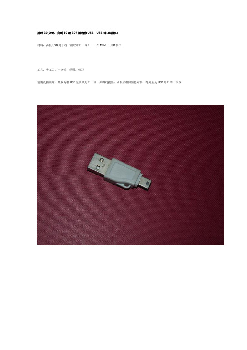
用时30分钟,自制10款307用迷你USB-USB母口转接口
材料:两根USB延长线(截取母口一端),一个MINI USB接口
工具:美工刀,电烙铁,焊锡,剪刀
前期没拍照片,截取两根USB延长线母口一端,并将线拨出,两根以相同颜色对接,得到全是USB母口的一根线
对接后用电烙铁焊接一下接口
我的工具
用胶布包扎一下接口
最后在外层加了两层胶布,防止平时使用时线头被拉扯脱落,一头接上优盘,一头接迷你USB转接口。
大功告成
家里有现成小口转大口的延长线(有的手机有这样的充电线),再加上根USB大口的延长线也可以拼成一根线。
有了标准的USB口,将来可以接很多东西了。
总的思路就是小口变大口。
TB上有这样的线,可惜偶没钱,所以找了现成的材料DIY一下,其实不难的。
常用USB转串口原理图设计大全

常用USB转串口芯片介绍串口, 芯片, USBPL2303符合USB1.1标准,价格3RMB.2 CP2102/CP2103简介Silicon Laboratories公司推出的USB接口与RS232接口转换器CP2102/CP2103是一款高度集成的USB-UART桥接器,提供一个使用最小化元件和PCB空间来实现RS232转换USB的简便解决方案。
如图1所示,CP2102/CP2103包含了一个USB功能控制器、USB收发器、振荡器和带有全部调制解调器控制信号的异步串行数据总线(UART),采用5 mm×5 mmMLP-28的封装。
CP2102/CP2103作为USB/RS232双向转换器,一方面可以从丰机接收USB数据并将其转换为RS232信息流格式发送给外设;另一方面可从RS232外设接收数据转换为USB数据格式传送至主机,其中包括控制和握手信号。
2.1 USB功能控制器和收发器2.2 异步串行数据总线(UART)接口CP2102/CP2103 UART接口包括TX (发送)和RX(接收)数据信号以及RTS、CTS、DSR、DTR、DCD和RI控制信号。
UART支持RTS/CTS、DSR/DTR和X-On/X-Off握手。
通过编程设置UART,支持各种数据格式和波特率。
在PC机的COM端口编程设置UART的数据格式和波特率。
表1为其数据格式和波特率。
2.3 内部EEPROMCP2102/CP2103内部集成有1个EEPROM,用于存储由设备制造商定义的USB供应商ID、产品ID、产品说明、电源参数、器件版本号和器件序列号等信息。
USB配置数据的定义是可选的。
如果EEPROM没有被OEM 的数据占用,则采用表1所示的默认配置数据。
注意,对于可能使用多个基于CP2102/CP2103连接到同一PC机的OEM应用来说,则需要专用的序列号。
内部EEPROM是通过USB编程设置的,允许OEM的USB配置数据和序列号可以在出厂和测试时直接写入系统板上的CP2102/CP2103。
USB转串口和并口的方法

如今呢是使用笔记本的人越来越多了,可是呢买了笔记本对于学习很多单片机比如说51或者AVR就不方便了。
因为大多数电脑都不带串并口了。
但是呢新出的笔记本上的USB接口是足够用的。
因而都想用USB转了串口或者并口就能方便单片机学习开发时的ISP编程或者JTAG仿真了。
其实很多单片机开发商和销售商都早就有了USBisp的配套软件和硬件了的,只不过都比较昂贵,而且技术资料多是保密的,对于自己小本学习单片机的人而言不免都希望能与价廉物美的USBISP烧写器,而且也多想自己动手做一个了。
网上公开的比较流行的支持51和AVR的烧写器是用ATMEL公司的MAGE8单片机做的,其机理也就是通过软件编程的方式将USB接口信号转换为并口信号以实现ISP的。
其原理图如下图:使用的是个名叫PROGISP的软件,我收集了制作的相关资料在压缩包中,有兴趣的朋友可以看看或者尝试一下。
但是呢我在这里主要并不是向大家介绍这个MAGE8做的USBISP下载线,因为它的编程软件很强大但是配置太灵活了,对于初学者,很容易配错相关设置,比如AVR的融丝位,弄不好可能将你的AVR单片机锁死了。
而且烧入MAGE8的固件有可能不支持51或AVR,找固件比较麻烦。
我要向大家推荐的另一种方案是用专门的USB转串口的USB芯片。
利用它制作一个USBISP下载线,而且支持51和AVR系列的单片机,功能算比较强的,电路也并不比M AGE8做的USBISP下载线难多少,只需要在主芯片外接晶振和几个电容电阻就是了。
这个方案就是利用国产的南京沁恒公司的CH341A芯片将USB转为并口直接实现ISP编程。
可以去南京沁恒公司网页申请到免费样片(注意要做USB下载线一定要申请CH341A,填写申请表时后缀字母A不能写错了)其电路图如下图:CH341 是一个USB 总线的转接芯片,通过USB总线提供异步串口、打印口、并口以及常用的2线和4 线等同步串行接口。
在异步串口方式下,CH341提供串口发送使能、串口接收就绪等交互式的速率控制信号以及常用的MODEM 联络信号,用于为计算机扩展异步串口,或者将普通的串口设备直接升级到US B 总线。
单路USB转多路串口方案分享

单路USB转多路串口方案分享串口,对于从事电子行业的朋友应该再也熟悉不过了,它是一种非常通用的设备通信的协议,大多数台式机箱都有RS232-DB9的接口,而且还有多个USB接口。
笔记本电脑通常只有3个USB口,而没有DB9端口,如果想使用串口功能,只能使用USB-TTL模块。
如果需要多个串口时,就要占用多个USB口,再加上鼠标、调试器等,PC提供的USB口就不够用了。
本文分享几种使用单USB口转多路串口的方案,串口之间相互独立,互不干扰。
1. CH9342单芯片实现双串口如果你最多只需要两路串口,那么CH9342是个不错的选择,它是一款单路USB转双串口芯片,提供两组全双工的9线异步串口UART0/1,用于为计算机扩展异步串口,或者将普通的串口设备升级到USB总线。
应用电路:评估板:2. CH9344单芯片实现4路串口如果两路串口不够用,不用担心,我们还有4路串口芯片,CH9344是一款单路USB转4串口控制芯片,提供4组全双工的异步串口UART0/1/2/3,用于为计算机扩展异步串口,或者将普通的串口设备升级到USB总线。
外部只需要一个30M的晶体和少量的电容即可使用,支持波特率1200-7.8125Mbps,LQFP-48封装。
应用电路:评估板:3. CH934X+CH438实现多串口如果需要更多的串口,可以试试CH934X配合CH438的方式。
CH943X是USB转多串口控制芯片,主要负责处理USB接口所有数据传输,并通过并行接口操作CH438,实现多个串口数据的接收和发送。
安装好驱动后,插入USB转串口模块,在电脑上会出现多个串口,这些串口操作方式上和电脑自带的串口一模一样,各个串口相互独立,互不干扰。
USB转多串口应用图如下:N可以为2、4、8、16,波特率支持1200-921600bps,各个串口操作与电脑自带硬件串口一模一样,相互独立,互不干扰。
在官网上并没有找到相关的应用资料,可能需要联系厂家获取资料。
电脑USB转TTL串口RS232串口模块

电脑USB转TTL串口/RS232串口模块对于一些学校、工业、科研客户来说,电脑的串口非常重要,很多设备都必须采用串口和电脑端软件连接,很多电路模块可以非常直观方便地利用串口调试软件进行调试,很多仪器必须通过串口进行通讯和数据交换。
但是目前笔记本电脑因为空间的限制和其他方面考虑的原因都没有串口,甚至一些台式电脑也取消了串口配置,这让我们迫切需要串口的客户非常苦恼。
USB转串口模块全称为USB to Serial port Module,它可以将USB接口虚拟成一个串口,解决客户无串口的苦恼。
现在市面上的USB转串品的设备可谓是琳琅满目,质量也是参差不齐。
造成这种现象的根本原因就在于控制芯片的不同。
现在USB转串口桥接芯片有很多,比如CP2102、FT232、PL2303等等。
但并非每一种芯片都可以用作ISP下载。
经过测试CP2102是不能下载的,而FT232可以下载,但其价格实在不菲。
最为适中的就是台湾生产的PL2303,可以稳定下载,并可以支持多种操作系统。
PL2303HX采用28脚贴片SOIC封装,工作频率为12MHZ,符合USB 1.1通信协议,可以直接将USB信号转换成串口信号,波特率从75~1228800,有22种波特率可以选择,并支持5、6、7、8、16共5种数据比特位,是一款相当不错的USB转串口芯片。
产品1:采用PL2303芯片的USB转TTL串口模块每个12元含一根4芯杜邦连接线这是我们用PL2303芯片开发的USB转串口模块,采用机器自动焊接都经人工检测,电路板只有30*16*7毫米,模块一共引出5根脚,引脚电平为TTL,引脚定义如下:+5V、P3.0 TXD 、P3.1 RXD 、GND 地线、+3.3V 。
其中+5V和+3.3V电源输出线一般情况下都不用的,不需要连接。
现在购买PL2303模块我们还赠送一根30厘米长的杜邦连接线,它一头是四位一体的插座可以直接插到我们的2303模块上,另一头是四个独立的杜邦头,可以灵活插到设备上,非常方便。
cp2104使用手册

cp2104使用手册CP2104是一款USB转串口芯片,常用于将USB接口转换为TTL或RS232电平的串口通信接口。
以下是CP2104的使用手册,供您参考:一、概述CP2104是一款USB转串口芯片,可以将USB接口转换为TTL或RS232电平的串口通信接口。
它具有体积小巧、使用方便、兼容性好等优点,广泛应用于各种需要USB转串口通信的场合。
二、工作原理CP2104的工作原理是通过USB总线与计算机进行通信,将USB信号转换为TTL或RS232电平的串口信号。
在USB信号转换为串口信号的过程中,CP2104内部集成了电平转换器、数据缓冲区、FIFO存储器等电路,以确保数据传输的稳定性和可靠性。
三、使用方法1.连接电路将CP2104的TTL或RS232接口通过电缆连接到需要通信的设备上,同时将CP2104的USB接口通过USB线连接到计算机上。
2.安装驱动程序在连接电路后,需要在计算机上安装CP2104的驱动程序。
驱动程序可以在芯片厂商的官方网站上下载,也可以在相关的操作系统上自动识别并安装。
3.配置串口参数在安装驱动程序后,可以在计算机上打开串口调试工具,如串口监视器、串口调试助手等,配置串口参数,如波特率、数据位、停止位、校验位等。
4.进行通信在配置好串口参数后,可以在计算机上通过串口调试工具向CP2104发送数据,同时也可以接收CP2104发送过来的数据。
四、注意事项1.在使用CP2104时,需要保证USB供电稳定,以免影响数据传输的稳定性。
2.在连接电路时,需要注意TTL或RS232接口的电平匹配问题,以免造成电路损坏。
3.在配置串口参数时,需要根据实际需要进行设置,以免影响数据传输的正确性。
4.在进行通信时,需要注意数据的传输速率和传输量,以免造成数据丢失或传输延迟。
USB转串口ch340选择经验

浅谈USB转串口USB是Universal serial bus的缩写,中文译作通用串行总线。
诞生于1994年,USB是目前最流行的一个外部总线标准,主要用于电脑与设备的连接通讯。
特点是传输速度快,支持热插拔。
串口就是串行通讯接口,诞生于1980年前后,是采用串行通讯方式的扩展接口,特点是通讯线路简单、数据一位一位的顺序传送,用一对传输线既可实现双向通讯。
优点是成本低、传输距离可达几千米,缺点是速度慢。
广泛用于工控设备,测量设备和通讯设备中。
由于USB转串口在计算机端就是一个COM串口,对于工程师而言,既能省掉操作USB的工作量,又能得到USB即插即用的优势,大幅度提高产品开发效率。
我们以市面上最常见的CH340为例,从USB转串口的实现、通讯、尺寸和应用4个方面来分别介绍下:2、特点●全速USB 设备接口,兼容USB V2.0。
●仿真标准串口,用于升级原串口外围设备,或者通过USB增加额外串口。
●计算机端Windows 操作系统下的串口应用程序完全兼容,无需修改。
●硬件全双工串口,内置收发缓冲区,支持通讯波特率50bps~2Mbps。
●支持常用的MODEM 联络信号RTS、DTR、DCD、RI、DSR、CTS。
●通过外加电平转换器件,提供RS232、RS485、RS422 等接口。
● CH340R 芯片支持IrDA 规范SIR红外线通讯,支持波特率2400bps到115200bps。
●内置固件,软件兼容CH341,可以直接使用CH341的VCP驱动程序。
●支持5V 电源电压和3.3V电源电压甚至3V 电源电压。
●提供SOP-16、SOP-8和SSOP-20以及ESSOP-10、MSOP-10无铅封装,兼容RoHS。
一,USB转串口的实现USB转串口即计算机端USB口转换为通用串口,一般为异步串口UART,既满足为缺少串口的计算机扩展异步串口,又可以将普通的串口设备升级到USB,还能将开发USB的难度降低至串口透明传输。
USB转串口原理及应用
USB转串口原理及应用USB转串口是指将USB接口转换成串口(或称为RS232接口)的方式。
USB(Universal Serial Bus,通用串行总线)是一种用于计算机之间连接和通信的通用接口。
而串口是一种用于计算机和外部设备之间进行异步串行通信的接口。
USB转串口的原理是通过内部的芯片实现的。
USB接口通常由USB控制器芯片和USB插座构成,而串口通常由UART(Universal Asynchronous Receiver and Transmitter,通用异步收发器)芯片实现。
所以,USB转串口的内部芯片实际上是将USB信号转换成UART信号,实现USB和串口之间的通信转换。
当计算机通过USB接口连接到USB转串口设备时,计算机会通过USB驱动程序与USB控制器芯片进行通信。
USB控制器芯片会将USB信号转换成串口信号,并通过UART芯片传送到串口接口上。
然后,外部设备可以通过串口接口与计算机进行通信,如串口打印机、串口调试工具等。
1.串口设备连接:许多传统的外部设备,如打印机、调制解调器、控制设备等,仍然使用串口进行通信。
通过USB转串口,这些设备可以与计算机连接,实现数据的传输和控制。
2.串口调试工具:在嵌入式系统和电子产品开发过程中,串口通常被用作调试接口。
通过USB转串口,开发人员可以使用计算机来进行调试和控制。
3.机器人控制:一些机器人和无人机使用串口进行通信。
通过USB转串口,计算机可以与这些设备进行通信,实现控制和数据传输。
4.工业自动化:在工业自动化领域,串口通常用于连接各种传感器、执行器和控制设备。
通过USB转串口,这些设备可以与计算机或控制系统进行通信,实现数据采集和控制。
5.特殊设备接口:有些特殊设备可能不直接支持USB接口,但支持串口接口。
通过USB转串口,可以将这些设备连接到计算机,实现数据传输和控制。
总之,USB转串口是一种将USB接口转换成串口接口的方式,通过内部芯片实现信号转换。
- 1、下载文档前请自行甄别文档内容的完整性,平台不提供额外的编辑、内容补充、找答案等附加服务。
- 2、"仅部分预览"的文档,不可在线预览部分如存在完整性等问题,可反馈申请退款(可完整预览的文档不适用该条件!)。
- 3、如文档侵犯您的权益,请联系客服反馈,我们会尽快为您处理(人工客服工作时间:9:00-18:30)。
Future Technology Devices International Ltd.FT232R USB UART ICThe FT232R is a USB to serial UART interface with the following advanced features:Single chip USB to asynchronous serial data transfer interface.Entire USB protocol handled on the chip. No USB specific firmware programming required.Fully integrated 1024 bit EEPROM storing device descriptors and CBUS I/O configuration.Fully integrated USB termination resistors.Fully integrated clock generation with no external crystal required plus optional clock output selection enabling a glue-less interface to external MCU or FPGA.Data transfer rates from 300 baud to 3 Mbaud (RS422, RS485, RS232 ) at TTL levels.128 byte receive buffer and 256 byte transmit buffer utilising buffer smoothing technology to allow for high data throughput.FTDI‟s royalty-free Virtual Com Port (VCP) and Direct (D2XX) drivers eliminate the requirement for USB driver development in most cases.Unique USB FTDIChip-ID™ feature.Configurable CBUS I/O pins.Transmit and receive LED drive signals.UART interface support for 7 or 8 data bits, 1 or 2 stop bits and odd / even / mark / space / no parity FIFO receive and transmit buffers for high data throughput.Synchronous and asynchronous bit bang interface options with RD# and WR# strobes.Device supplied pre-programmed with unique USB serial number.Supports bus powered, self powered and high-power bus powered USB configurations.Integrated +3.3V level converter for USB I/O.Integrated level converter on UART and CBUS for interfacing to between +1.8V and +5V logic.True 5V/3.3V/2.8V/1.8V CMOS drive output and TTL input.Configurable I/O pin output drive strength.Integrated power-on-reset circuit.Fully integrated AVCC supply filtering - no external filtering required.UART signal inversion option.+3.3V (using external oscillator) to +5.25V (internal oscillator) Single Supply Operation. Low operating and USB suspend current.Low USB bandwidth consumption.UHCI/OHCI/EHCI host controller compatible.USB 2.0 Full Speed compatible.-40°C to 85°C extended operating temperature range.Available in compact Pb-free 28 Pin SSOP and QFN-32 packages (both RoHS compliant).Neither the whole nor any part of the information contained in, or the product described in this manual, may be adapted or reproduced in any material or electronic form without the prior written consent of the copyright holder. This product and its documentation are supplied on an as-is basis and no warranty as to their suitability for any particular purpose is either made or implied. Future Technology Devices International Ltd will not accept any claim for damages howsoever arising as a result of use or failure of this product. Your statutory rights are not affected. This product or any variant of it is not intended for use in any medical appliance, device or system in which the failure of the product might reasonably be expected to result in personal injury. This document provides preliminary information that may be subject to change without notice. No freedom to use patents or other intellectual property rights is implied by the publication of this document. Future Technology Devices International Ltd, Unit 1, 2 Seaward Place, Centurion Business Park, Glasgow G41 1HH United Kingdom. Scotland Registered Company Number: SC1366401Typical ApplicationsUSB to RS232/RS422/RS485 Converters Upgrading Legacy Peripherals to USBCellular and Cordless Phone USB data transfer cables and interfacesInterfacing MCU/PLD/FPGA based designs to USBUSB Audio and Low Bandwidth Video data transferPDA to USB data transferUSB Smart Card ReadersUSB Instrumentation USB Industrial ControlUSB MP3 Player InterfaceUSB FLASH Card Reader and Writers Set Top Box PC - USB interfaceUSB Digital Camera InterfaceUSB Hardware ModemsUSB Wireless ModemsUSB Bar Code ReadersUSB Software and Hardware Encryption Dongles1.1Driver SupportRoyalty free VIRTUAL COM PORT (VCP) DRIVERS for...Windows 98, 98SE, ME, 2000, Server 2003, XP and Server 2008Windows 7 32,64-bitWindows XP and XP 64-bitWindows Vista and Vista 64-bitWindows XP EmbeddedWindows CE 4.2, 5.0 and 6.0Mac OS 8/9, OS-XLinux 2.4 and greater Royalty free D2XX Direct Drivers(USB Drivers + DLL S/W Interface) Windows 98, 98SE, ME, 2000, Server 2003, XP and Server 2008Windows 7 32,64-bitWindows XP and XP 64-bitWindows Vista and Vista 64-bitWindows XP EmbeddedWindows CE 4.2, 5.0 and 6.0Linux 2.4 and greaterThe drivers listed above are all available to download for free from FTDI website (). Various 3rd party drivers are also available for other operating systems - see FTDI website () for details.For driver installation, please refer to /Documents/InstallGuides.htm1.2Part NumbersNote: Packing codes for xxxx is:- Reel: Taped and Reel, (SSOP is 2,000pcs per reel, QFN is 6,000pcs per reel).- Tube: Tube packing, 47pcs per tube (SSOP only)- Tray: Tray packing, 490pcs per tray (QFN only)For example: FT232RQ-Reel is 6,000pcs taped and reel packingThe FT232R is fully compliant with the USB 2.0 specification and has been given the USB-IF Test-ID (TID) 40680004.Figure 2.1 FT232R Block DiagramFor a description of each function please refer to Section 4.OCSI VCCDBUS0DBUS1DBUS2DBUS3DBUS4DBUS5DBUS6DBUS7CBUS0CBUS2CBUS3TEST GNDCBUS1CBUS4Table of Contents1Typical Applications (2)1.1Driver Support (2)1.2Part Numbers (2)Note: Packing codes for xxxx is: (2)1.3USB Compliant (3)2FT232R Block Diagram (4)3Device Pin Out and Signal Description (7)3.128-LD SSOP Package (7)3.2SSOP Package Pin Out Description (7)3.3QFN-32 Package (10)3.4QFN-32 Package Signal Description (10)3.5CBUS Signal Options (13)4Function Description (14)4.1Key Features (14)4.2Functional Block Descriptions (15)5Devices Characteristics and Ratings (17)5.1Absolute Maximum Ratings (17)5.2DC Characteristics (18)5.3EEPROM Reliability Characteristics (21)5.4Internal Clock Characteristics (21)6USB Power Configurations (23)6.1USB Bus Powered Configuration (23)6.2Self Powered Configuration (24)6.3USB Bus Powered with Power Switching Configuration (25)6.4USB Bus Powered with Selectable External Logic Supply (26)7Application Examples (27)7.1USB to RS232 Converter (27)7.2USB to RS485 Coverter (28)7.3USB to RS422 Converter (29)7.4USB to MCU UART Interface (30)7.5LED Interface (31)7.6Using the External Oscillator (32)8Internal EEPROM Configuration (33)9Package Parameters (35)9.1SSOP-28 Package Dimensions (35)9.3QFN-32 Package Typical Pad Layout (37)9.4QFN-32 Package Typical Solder Paste Diagram (37)9.5Solder Reflow Profile (38)10Contact Information (39)Appendix A – References (40)Appendix B - List of Figures and Tables (41)Appendix C - Revision History (43)3 Device Pin Out and Signal Description 3.1 28-LD SSOP PackageFigure 3.1 SSOP Package Pin Out and Schematic Symbol3.2 SSOP Package Pin Out DescriptionNote: The convention used throughout this document for active low signals is the signal name followed by a #USBDPUSBDM3V3OUT GND RESET#VCC GND NCAGND TEST OSCI OSCO CBUS1CBUS0Notes:1.The minimum operating voltage VCC must be +4.0V (could use VBUS=+5V) when using theinternal clock generator. Operation at +3.3V is possible using an external crystal oscillator.2.For details on how to use an external crystal, ceramic resonator, or oscillator with the FT232R,please refer Section 7.63.When used in Input Mode, the input pins are pulled to VCCIO via internal 200kΩ resistors. Thesepins can be programmed to gently pull low during USB suspend (PWREN# = “1”) by setting an option in the internal EEPROM.Figure 3.2 QFN-32 Package Pin Out and schematic symbol3.4 QFN-32 Package Signal Description3225241716981123456782526272829303132USBDPUSBDM3V3OUTRESET#VCC NC AGNDTESTOSCIOSCOCBUS1CBUS0TXDRTS#RXD DTR#VCCIO RI#GND NC DSR#DCD#CTS#CBUS4CBUS2CBUS3GNDGND NCNCNCNCNotes:1.The minimum operating voltage VCC must be +4.0V (could use VBUS=+5V) when using theinternal clock generator. Operation at +3.3V is possible using an external crystal oscillator.2.For details on how to use an external crystal, ceramic resonator, or oscillator with the FT232R,please refer to Section 7.6.3.When used in Input Mode, the input pins are pulled to VCCIO via internal 200kΩ resistors. Thesepins can be programmed to gently pull low during USB suspend (PWREN# = “1”) by setting an option in the internal EEPROM.The following options can be configured on the CBUS I/O pins. CBUS signal options are common to both package versions of the FT232R. These options can be configured in the internal EEPROM using the software utility FT_PPROG or MPROG, which can be downloaded from the FTDI Utilities(). The default configuration is described in Section 8.* PWREN# must be used with a 10kΩ resistor pull up.**When in USB suspend mode the outputs clocks are also suspended.The FT232R is a USB to serial UART interface device which simplifies USB to serial designs and reduces external component count by fully integrating an external EEPROM, USB termination resistors and an integrated clock circuit which requires no external crystal, into the device. It has been designed to operate efficiently with a USB host controller by using as little as possible of the total USB bandwidth available.4.1Key FeaturesFunctional Integration. Fully integrated EEPROM, USB termination resistors, clock generation, AVCC filtering, POR and LDO regulator.Configurable CBUS I/O Pin Options. The fully integrated EEPROM allows configuration of the Control Bus (CBUS) functionality, signal inversion and drive strength selection. There are 5 configurable CBUSI/O pins. These configurable options are1.TXDEN - transmit enable for RS485 designs.2.PWREN# - Power control for high power, bus powered designs.3.TXLED# - for pulsing an LED upon transmission of data.4.RXLED# - for pulsing an LED upon receiving data.5.TX&RXLED# - which will pulse an LED upon transmission OR reception of data.6.SLEEP# - indicates that the device going into USB suspend mode.7.CLK48 / CLK24 / CLK12 / CLK6 - 48MHz, 24MHz, 12MHz, and 6MHz clock output signaloptions.The CBUS pins can also be individually configured as GPIO pins, similar to asynchronous bit bang mode. It is possible to use this mode while the UART interface is being used, thus providing up to 4 general purpose I/O pins which are available during normal operation. An application note, AN232R-01,available from FTDI website () describes this feature.The CBUS lines can be configured with any one of these output options by setting bits in the internal EEPROM. The device is supplied with the most commonly used pin definitions pre-programmed - see Section 8 for details.Asynchronous Bit Bang Mode with RD# and WR# Strobes. The FT232R supports FTDI‟s previous chip generation bit-bang mode. In bit-bang mode, the eight UART lines can be switched from the regular interface mode to an 8-bit general purpose I/O port. Data packets can be sent to the device and they will be sequentially sent to the interface at a rate controlled by an internal timer (equivalent to the baud rate pre-scaler). With the FT232R device this mode has been enhanced by outputting the internal RD# and WR# strobes signals which can be used to allow external logic to be clocked by accesses to the bit-bang I/O bus. This option will be described more fully in a separate application note available from FTDI website ().Synchronous Bit Bang Mode. The FT232R supports synchronous bit bang mode. This mode differs from asynchronous bit bang mode in that the interface pins are only read when the device is written to. This makes it easier for the controlling program to measure the response to an output stimulus as the data returned is synchronous to the output data. An application note, AN232R-01,available from FTDI website () describes this feature.FTDIChip-ID™. The FT232R also includes the new FTDIChip-ID™ security dongle feature. This FTDIChip-ID™ feature allows a unique number to be burnt into each device during manufacture. This number cannot be reprogrammed. This number is only readable over USB and forms a basis of a security dongle which can be used to protect any customer application software being copied. This allows the possibility of using the FT232R in a dongle for software licensing. Further to this, a renewable license scheme can be implemented based on the FTDIChip-ID™ number when encrypted with other information. This encrypted number can be stored in the user area of the FT232R internal EEPROM, and can be decrypted, then compared with the protected FTDIChip-ID™ to verify that a license is valid. Web based applications can be used to maintain product licensing this way. An application note, AN232R-02, available from FTDI website () describes this feature.The FT232R is capable of operating at a voltage supply between +3.3V and +5V with a nominal operational mode current of 15mA and a nominal USB suspend mode current of 70µA. This allows greater margin for peripheral designs to meet the USB suspend mode current limit of 2.5mA. An integrated level converter within the UART interface allows the FT232R to interface to UART logic running at +1.8V, 2.5V, +3.3V or +5V.The following paragraphs detail each function within the FT232R. Please refer to the block diagram shown in Figure 2.1Internal EEPROM. The internal EEPROM in the FT232R is used to store USB Vendor ID (VID), Product ID (PID), device serial number, product description string and various other USB configuration descriptors. The internal EEPROM is also used to configure the CBUS pin functions. The FT232R is supplied with the internal EEPROM pre-programmed as described in Section 8. A user area of the internal EEPROM is available to system designers to allow storing additional data. The internal EEPROM descriptors can be programmed in circuit, over USB without any additional voltage requirement. It can be programmed using the FTDI utility software called MPROG, which can be downloaded from FTDI Utilities on the FTDI website ().+3.3V LDO Regulator. The +3.3V LDO regulator generates the +3.3V reference voltage for driving the USB transceiver cell output buffers. It requires an external decoupling capacitor to be attached to the3V3OUT regulator output pin. It also provides +3.3V power to the 1.5kΩ internal pull up resistor on USBDP. The main function of the LDO is to power the USB Transceiver and the Reset Generator Cells rather than to power external logic. However, it can be used to supply external circuitry requiring a+3.3V nominal supply with a maximum current of 50mA.USB Transceiver. The USB Transceiver Cell provides the USB 1.1 / USB 2.0 full-speed physical interface to the USB cable. The output drivers provide +3.3V level slew rate control signalling, whilst a differential input receiver and two single ended input receivers provide USB data in, Single-Ended-0 (SE0) and USB reset detection conditions respectfully. This function also incorporates the internal USB series termination resistors on the USB data lines and a 1.5kΩ pull up resistor on USBDP.USB DPLL. The USB DPLL cell locks on to the incoming NRZI USB data and generates recovered clock and data signals for the Serial Interface Engine (SIE) block.Internal 12MHz Oscillator - The Internal 12MHz Oscillator cell generates a 12MHz reference clock. This provides an input to the x4 Clock Multiplier function. The 12MHz Oscillator is also used as the reference clock for the SIE, USB Protocol Engine and UART FIFO controller blocks.Clock Multiplier / Divider. The Clock Multiplier / Divider takes the 12MHz input from the Internal Oscillator function and generates the 48MHz, 24MHz, 12MHz and 6MHz reference clock signals. The 48Mz clock reference is used by the USB DPLL and the Baud Rate Generator blocks.Serial Interface Engine (SIE). The Serial Interface Engine (SIE) block performs the parallel to serial and serial to parallel conversion of the USB data. In accordance with the USB 2.0 specification, it performs bit stuffing/un-stuffing and CRC5/CRC16 generation. It also checks the CRC on the USB data stream.USB Protocol Engine. The USB Protocol Engine manages the data stream from the device USB control endpoint. It handles the low level USB protocol requests generated by the USB host controller and the commands for controlling the functional parameters of the UART in accordance with the USB 2.0 specification chapter 9.FIFO RX Buffer (128 bytes). Data sent from the USB host controller to the UART via the USB data OUT endpoint is stored in the FIFO RX (receive) buffer. Data is removed from the buffer to the UART transmit register under control of the UART FIFO controller. (Rx relative to the USB interface).FIFO TX Buffer (256 bytes). Data from the UART receive register is stored in the TX buffer. The USB host controller removes data from the FIFO TX Buffer by sending a USB request for data from the device data IN endpoint. (Tx relative to the USB interface).UART FIFO Controller. The UART FIFO controller handles the transfer of data between the FIFO RX and TX buffers and the UART transmit and receive registers.UART Controller with Programmable Signal Inversion and High Drive. Together with the UART FIFO Controller the UART Controller handles the transfer of data between the FIFO RX and FIFO TX buffers and the UART transmit and receive registers. It performs asynchronous 7 or 8 bit parallel to serial and serial to parallel conversion of the data on the RS232 (or RS422 or RS485) interface.Control signals supported by UART mode include RTS, CTS, DSR, DTR, DCD and RI. The UART Controller also provides a transmitter enable control signal pin option (TXDEN) to assist with interfacing to RS485 transceivers. RTS/CTS, DSR/DTR and X ON / X OFF handshaking options are also supported. Handshaking is handled in hardware to ensure fast response times. The UART interface also supports the RS232 BREAK setting and detection conditions.strength capability. Both these features are configurable in the EEPROM.Baud Rate Generator - The Baud Rate Generator provides a 16x clock input to the UART Controller from the 48MHz reference clock. It consists of a 14 bit pre-scaler and 3 register bits which provide fine tuning of the baud rate (used to divide by a number plus a fraction or “sub-integer”). This determines the baud rate of the UART, which is programmable from 183 baud to 3 Mbaud.The FT232R supports all standard baud rates and non-standard baud rates from 183 Baud up to 3 Mbaud. Achievable non-standard baud rates are calculated as follows -Baud Rate = 3000000 / (n + x)where …n‟ can be any integer between 2 and 16,384 ( = 214) and …x’ can be a sub-integer of the value 0, 0.125, 0.25, 0.375, 0.5, 0.625, 0.75, or 0.875. When n = 1, x = 0, i.e. baud rate divisors with values between 1 and 2 are not possible.This gives achievable baud rates in the range 183.1 baud to 3,000,000 baud. When a non-standard baud rate is required simply pass the required baud rate value to the driver as normal, and the FTDI driver will calculate the required divisor, and set the baud rate. See FTDI application note AN232B-05 on the FTDI website () for more details.RESET Generator - The integrated Reset Generator Cell provides a reliable power-on reset to the device internal circuitry at power up. The RESET# input pin allows an external device to reset the FT232R. RESET# can be tied to VCC or left unconnected if not being used.5.1Absolute Maximum RatingsThe absolute maximum ratings for the FT232R devices are as follows. These are in accordance with the Absolute Maximum Rating System (IEC 60134). Exceeding these may cause permanent damage to the device.* If devices are stored out of the packaging beyond this time limit the devices should be baked before use. The devices should be ramped up to a temperature of +125°C and baked for up to 17 hours.DC Characteristics (Ambient Temperature = -40°C to +85°C)** Only input pins have an internal 200KΩ pull-up resistor to VCCIO5.3EEPROM Reliability CharacteristicsThe internal 1024 Bit EEPROM has the following reliability characteristics:5.4Internal Clock CharacteristicsThe internal Clock Oscillator has the following characteristics:Note 1: Equivalent to +/-1667ppmNote1: When supplied, the FT232R is configured to use its internal clock oscillator. These characteristics only apply when an external oscillator or crystal is used.The following sections illustrate possible USB power configurations for the FT232R. The illustrations have omitted pin numbers for ease of understanding since the pins differ between the FT232RL and FT232RQ package options.All USB power configurations illustrated apply to both package options for the FT232R device. Please refer to Section 3 for the package option pin-out and signal descriptions.6.1USB Bus Powered ConfigurationFigure 6.1 Bus Powered ConfigurationFigure 6.1 Illustrates the FT232R in a typical USB bus powered design configuration. A USB bus powered device gets its power from the USB bus. Basic rules for USB bus power devices are as follows –i)On plug-in to USB, the device should draw no more current than 100mA.ii)In USB Suspend mode the device should draw no more than 2.5mA.iii) A bus powered high power USB device (one that draws more than 100mA) should use one of the CBUS pins configured as PWREN# and use it to keep the current below 100mA on plug-inand 2.5mA on USB suspend.iv) A device that consumes more than 100mA cannot be plugged into a USB bus powered hub.v)No device can draw more than 500mA from the USB bus.The power descriptors in the internal EEPROM of the FT232R should be programmed to match the current drawn by the device.A ferrite bead is connected in series with the USB power supply to reduce EMI noise from the FT232R and associated circuitry being radiated down the USB cable to the USB host. The value of the Ferrite Bead depends on the total current drawn by the application. A suitable range of Ferrite Beads is available from Steward (), for example Steward Part # MI0805K400R-10.Note: If using PWREN# (available using the CBUS) the pin should be pulled to VCCIO using a 10kΩresistor.Figure 6.2 Self Powered ConfigurationFigure 6.2 illustrates the FT232R in a typical USB self powered configuration. A USB self powered device gets its power from its own power supply, VCC, and does not draw current from the USB bus. The basic rules for USB self powered devices are as follows –i) A self powered device should not force current down the USB bus when the USB host or hubcontroller is powered down.ii) A self powered device can use as much current as it needs during normal operation and USB suspend as it has its own power supply.iii) A self powered device can be used with any USB host, a bus powered USB hub or a self powered USB hub.The power descriptor in the internal EEPROM of the FT232R should be programmed to a value of zero (self powered).In order to comply with the first requirement above, the USB bus power (pin 1) is used to control the RESET# pin of the FT232R device. When the USB host or hub is powered up an internal 1.5kΩ resistor on USBDP is pulled up to +3.3V (generated using the 4K7 and 10k resistor network), thus identifying the device as a full speed device to the USB host or hub. When the USB host or hub is powered off, RESET# will be low and the FT232R is held in reset. Since RESET# is low, the internal 1.5kΩ resistor is not pulled up to any power supp ly (hub or host is powered down), so no current flows down USBDP via the 1.5kΩ pull-up resistor. Failure to do this may cause some USB host or hub controllers to power up erratically. Figure 6.2 illustrates a self powered design which has a +4V to +5.25V supply.Note:1.When the FT232R is in reset, the UART interface I/O pins are tri-stated. Input pins have internal200kΩ pull-up resistors to VCCIO, so they will gently pull high unless driven by some externallogic.2.When using internal FT232R oscillator the VCC supply voltage range must be +4.0V to 5.25V.3.When using external oscillator the VCC supply voltage range must be +3.3V to 5.25VAny design which interfaces to +3.3 V or +1.8V would be having a +3.3V or +1.8V supply toP-Channel PowerMOSFETFigure 6.3 Bus Powered with Power Switching ConfigurationA requirement of USB bus powered applications, is when in USB suspend mode, the application draws a total current of less than 2.5mA. This requirement includes external logic. Some external logic has the ability to power itself down into a low current state by monitoring the PWREN# signal. For external logic that cannot power itself down in this way, the FT232R provides a simple but effective method of turning off power during the USB suspend mode.Figure 6.3 shows an example of using a discrete P-Channel MOSFET to control the power to external logic. A suitable device to do this is an International Rectifier () IRLML6402, or equivalent. It is recommended that a “soft start” circuit consisting of a 1kΩ series resistor and a 0.1μF capacitor is used to limit the current surge when the MOSFET turns on. Without the soft start circuit it is possible that the transient power surge, caused when the MOSFET switches on, will reset the FT232R or the USB host/hub controller. The soft start circuit example shown in Figure 6.3 powers up with a slew rate of approximaely12.5V/ms. Thus supply voltage to external logic transitions from GND to +5V in approximately 400 microseconds.As an alternative to the MOSFET, a dedicated power switch IC with inbuilt “soft-start” can be used. A suitable power switch IC for such an application is the Micrel () MIC2025-2BM or equivalent.With power switching controlled designs the following should be noted:i)The external logic to which the power is being switched should have its own reset circuitry toautomatically reset the logic when power is re-applied when moving out of suspend mode.ii)Set the Pull-down on Suspend option in the internal FT232R EEPROM.iii)One of the CBUS Pins should be configured as PWREN# in the internal FT232R EEPROM, and used to switch the power supply to the external circuitry. This should be pulled high through a 10 kΩ resistor.iv)For USB high-power bus powered applications (one that consumes greater than 100mA, and up to 500mA of current from the USB bus), the power consumption of the application must be set in the Max Power field in the internal FT232R EEPROM. A high-power bus powered application uses the descriptor in the internal FT232R EEPROM to inform the system of its power requirements.3.3V or 5VSupply toFigure 6.4 USB Bus Powered with +3.3V or +5V External Logic Power SupplyFigure 6.4 illustrates a USB bus power application with selectable external logic supply. The external logic can be selected between +3.3V and +5V using the jumper switch. This jumper is used to allow theFT232R to be interfaced with a +3.3V or +5V logic devices. The VCCIO pin is either supplied with +5V from the USB bus (jumper pins1 and 2 connected), or from the +3.3V output from the FT232R 3V3OUT pin (jumper pins 2 and 3 connected). The supply to VCCIO is also used to supply external logic.With bus powered applications, the following should be noted:i)To comply with the 2.5mA current supply limit during USB suspend mode, PWREN# orSLEEP# signals should be used to power down external logic in this mode. If this is notpossible, use the configuration shown in Section 6.3.ii)The maximum current sourced from the USB bus during normal operation should not exceed 100mA, otherwise a bus powered design with power switching (Section 6.3) should be used. Another possible configuration could use a discrete low dropout (LDO) regulator which is supplied by the 5V on the USB bus to supply between +1.8V and +2.8V to the VCCIO pin and to the external logic. In this case VCC would be supplied with the +5V from the USB bus and the VCCIO would be supplied from the output of the LDO regulator. This results in the FT232R I/O pins driving out at between +1.8V and+2.8V logic levels.For a USB bus powered application, it is important to consider the following when selecting the regulator:i)The regulator must be capable of sustaining its output voltage with an input voltage of+4.35V. An Low Drop Out (LDO) regulator should be selected.ii)The quiescent current of the regulator must be low enough to meet the total current requirement of <= 2.5mA during USB suspend mode.A suitable series of LDO regulators that meets these requirements is the MicroChip/Telcom() TC55 series of devices. These devices can supply up to 250mA current and have a quiescent current of under 1μA.。