CY7C1051DV33芯片手册
CY7C025资料

Notes: 1. BUSY is an output in master mode and an input in slave mode. 2. I/O0 –I/O8 on the CY7C0241/0251. 3. I/O9 –I/O17 on the CY7C0241/0251. 4. A12L on the CY7C025/0251. 5. A12R on the CY7C025/0251.
CY7C024/0241 CY7C025/0251
Logic Block DiagramL L源自R/W R UBRL
LBR CE R OE R
OE L
[3] I/O 8L – I/O 15L
I/O 0L – I/O 7L
[2] [1]
I/O CONTROL
I/O CONTROL
I/O8R – I/O15R[3] I/O 0R– I/O 7R [2]
Document #: 38-06035 Rev. *C
Page 2 of 21
元器件交易网
CY7C024/0241 CY7C025/0251
Pin Configurations (continued)
OEL VCC R/WL SEML CEL UBL LBL NC [4] A11L A10L
INTERRUPT SEMAPHORE ARBITRATION
CE R OE R UB R LB R R/W R SEM R
M/S
INTR
Pin Configurations
84-Pin PLCC Top View
SEM L CEL UB L GND I/O 1L I/O 0L OE L V CC LB L NC [4] A11L R/WL I/O 7L I/O 6L I/O 5L I/O 4L I/O 3L I/O 2L A 10L A A 8L A7L A6L A5L A4L A3L A2L A1L A0L INTL BUSYL GND M/S BUSYR INTR A0R A1R A2R A3R A4R A5R A6R
CTM1051(A)MG超小体积高速CAN隔离收发器说明书
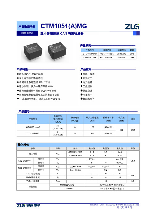
输入特性参数 符号 条件 最小值 典型值 最大值 单位输入电压V CCCTM1051AMG 3.15 3.3 3.45 VDC CTM1051MG4.75 55.25 TXD 逻辑电平 高电平 V IH 0.7V CC -- V CC +0.5 低电平 V IL 0 -- 0.3V CC RXD 逻辑电平高电平 V OH I RXD =-1.5mA V CC -0.4 V CC -0.2 -- 低电平V OL I RXD =1.5mA-- 0.2 0.4 TXD 驱动电流 I T 2 -- -- mA RXD 输出电流 I R -- -- 10 TXD 上拉电阻 R TXD--10--kΩ 串行接口CTM1051AMG 3.3V 标准CAN 控制器接口 CTM1051MG5V 标准CAN 控制器接口产品特性—————————————————◆符合ISO 11898-2标准 ◆未上电节点不影响总线 ◆单网络最多可连接110个节点 ◆超小体积,仅为一般产品的40% ◆外壳及灌封材料符合UL94 V-0标准 ◆具有极低电磁辐射和高的抗电磁干扰性 ◆高低温特性好,满足工业级产品要求CTM1051(A)MG产品数据手册超小体积高速CAN 隔离收发器产品系列————————————————产品型号 温度范围 隔离耐压 封装 CTM1051AMG -40℃~+105℃ 2500VDC DIP8 CTM1051MG-40℃~+105℃2500VDCDIP8产品应用————————————————◆仪器、仪表 ◆石油化工 ◆电力监控 ◆工业控制 ◆轨道交通 ◆汽车电子 ◆智能家居等Data Sheet产品型号———————————————————————————————————————产品型号电源电压 (电压范围) (VDC) 静态电流 (mA,Typ)最大工作电流(mA)传输波特率 (bps) 节点数 (pcs)类型CTM1051AMG 3.3 (3.15-3.45) 8 120 40k~1M110高速CTM1051MG5(4.75-5.25)99040k~1M输出特性参数符号条件最小值典型值最大值单位显性电平(逻辑0)CANH V(OD)CANH R L=60Ω 2.75 3.5 4.5VDC CANL V(OD)CANL R L=60Ω 0.5 1.5 2.25 隐性电平(逻辑1)CANH V(OR)CANH no load 2 2.5 3CANL V(OR)CANL no load 2 2.5 3 差分电平显性(逻辑0) V diff(d)R L=60Ω 1.5 2 3隐性(逻辑1) V diff(r)no load -0.05 0 0.05 总线引脚最大耐压V X CANH、CANL -40 -- +40总线引脚漏电流I LV CC=0VV CANH/L=5V-5 -- +5 µA CAN总线接口符合ISO 11898-2 标准,双绞线输出传输特性参数名称符号条件最小值典型值最大值单位数据延时TXD发送延时t T R L=60Ω -- 60 --ns RXD接收延时t R R L=60Ω -- 80 --循环延迟t PD(TXD-RXD)R L=60Ω -- 140 210 TXD显性超时时间t to(dom)TXD V TXD=0V 0.3 -- 3.8 ms极限特性参数条件最小值典型值最大值单位输入冲击电压(1)(1s,max)CTM1051AMG -0.7 -- 5VDCCTM1051MG -0.7 -- 7 引脚焊接温度焊点距离外壳1.5mm,10秒-- -- 300 ℃热插拔不支持一般特性参数条件最小值典型值最大值单位隔离电压输入-输出,时间1分钟,漏电流小于1mA2500 -- -- VDC 绝缘电阻输入-输出,绝缘电压500VDC 1 -- -- GΩ封装尺寸12.80×10.20×7.70 mm外壳材料黑色阻燃塑胶外壳,符合UL94 V-0标准环境特性参数名称条件最小值典型值最大值单位工作温度-40 -- +105℃存储温度-55 -- +125外壳温升Ta=25℃-- 15 25存储湿度无凝结-- -- 95 %冷却方式自然空冷EMC特性EMS静电放电抗扰度IEC/EN 61000-4-2 Contact ±4kV (裸机,总线端口) (2)Perf. Criteria B脉冲群抗扰度IEC/EN 61000-4-4 ±2kV(裸机,总线端口) (2)Perf. Criteria B浪涌抗扰度IEC/EN 61000-4-5 共模±2kV(裸机,总线端口) (2)Perf. Criteria BIEC/EN 61000-4-5 差模±2kV,共模±4kV(应用电路图3、图4)(3)Perf. Criteria B 传导骚扰抗扰度IEC/EN 61000-4-6 3Vr.m.s(裸机) Perf. Criteria A注:(1)输入电压不能超过所规定范围值,否则可能会造成永久性不可恢复的损坏。
柯拉尔(Carrier)33CS-33PS年型 PremierLink retrofit 控制器说明

Copyright 2007 Carrier CorporationForm 33CS-33PSThe PremierLink retrofit controllers offer:•continuous monitoring and regulation of the rooftop unit•compatibility with Carrier diagnostic display tools•other devices can read and write data to the controller•ability to connect unit to the Carrier Comfort Network® (CCN) systemFeatures/BenefitsThe PremierLink retrofit rooftop controller is an intelligent control thatcontinuously monitors and regulates rooftop operation with reliability and precision that minimizes downtime to ensure maximum occupant comfort.The PremierLink controller is compati-ble with the Carrier ComfortNetwork (CCN) system. Carrier’s diag-nostic standard tier display tools such as System Pilot™ or Touch Pilot™ device can be used with the PremierLink con-troller. User interfaces include the CCN Service Tool, ComfortVIEW™ and ComfortWORKS ® software.When the PremierLink controller is used as part of the CCN system, otherdevices such as the CCN data transfer, 3V™ linkage coordinator, or Comfort Controller can read data from or write data to the retrofit controller.PREMIERLINK™Retrofit RooftopController33CSPREMLKProductSpecificationa33-91472Extensive control capabilitiesThe 33CSPREMLK retrofit controller provides the following features and benefits:•provides software clock and local occupancy schedule for local occu-pancy control (requires time broad-caster and hardware clock from another device in the system)•uses remote timeclock input to pro-vide occupancy control through exter-nal contacts or this input can be reconfigured for use with a door or window switch to disable heating and cooling if a door or window is left open•provides continous or intermittent fan operation in the occupied mode•features supply air temperature limit-ing and integrated safeties for DX (direct expansion), gas, electric and heat pump units•provides field tests that enables the user to check output points and verify their functionality•controls two stages of DX cooling to maintain space temperature set point •ability to provide occupied and unoc-cupied dehumidification•controls up to 3 stages of gas heat or combination of mechanical and elec-tric heat to maintain space tempera-ture set point•ability to control exhaust fan based on economizer or occupancy on 2-stage heat units•ability to control reversing valve on heat pump units•provides temperature compensated start of heating or cooling to achieve set point by the start of the sched- uled occupied time•provides alarms for analog tempera-ture input(s) out of range•provides alarm for space tempera-ture deviation from desired set point •adjustable filter maintenance timer •allows manual and system overrides of selected input/output channels•supports CCN remote timed override, set point adjustment and manual fan control override•provides Broadcast Acknowledger capability for CCN (configuration)•conforms to the general require- ments for CCN devices•modulates control of economizer to assist mechanical cooling without adversely affecting compressor performance•provides ventilation monitoring with optional CO 2 ventilation sensor •compatible with T55 space sensor and T56 space sensor with set point adjustment, timed override and ser-vice port jack•compatibility with T58 communicat-ing sensor provides set point adjust-ment, timed override, force fan, and read equipment mode•compatibility with System Pilot as a communicating sensor providing set point adjustment, timed override, and a user interface for programming, configuration, and monitoring and forcing points•support a local or global occupancy schedule or remote start input status to determine occupancy•individual fan start delay for each Premierlink™ board upon occupancy change.Available for wide range of rooftop applicationsThe PremierLink controller is available as a field retrofit application and can control one or several rooftop units with (multiple controllers) from 3 to 25 tons. In addition, it has an integrated economizer controller that eliminates the need for a separate cir-cuit board.The PremierLink controller can be installed on the following Carrier rooftop units: 48/50HE (2 to 5 tons), 50HEQ (2 to 5 tons), 48/50HJ (3 to 25 tons),50HJQ (3 to 15 tons), 48TF/50TFF (3 to 121/2 tons), 50TFQ (3 to 10 tons), 48/50TJ (121/2 to 25 tons), and 48/50TM (3 to 25 tons). Other Carrier equipment and non-Carrier equipment can also be controlled by PremierLink controller. Con-tact a Carrier Factory Sales representative for more information.Flexibility for every applicationThe PremierLink controller is an ad- vanced microprocessor-based control. PremierLink is precision controlled to send heating and cooling only when needed, reducing energy use and operat-ing costs.Carrier linkage compatibilityWhen used as the air source for a 3V™ zoning system, the PremierLink control-ler will use occupancy schedules, zone temperature, and set points from the 3V linkage coordinator. The PremierLink controller provides the 3V linkage coordi-nator with the unit’s operating mode and supply-air temperature to provide coordi-nation of the individual member zone's local mode with the system mode.Additional control featuresThe PremierLink controller provides addi-tional control features such as Occupied/Unoccupied schedulinginitialized via the network. The Premier-Link controller offers override invoked from a wall sensor during unoccupied hours from 1 to 4 hours in 1-hour increments.The PremierLink controller offers venti-lation monitoring with an optional CO 2 ventilation sensor. The CO 2 ventilation sensor measures the amount of ventilation needed by the space and a proportional integral derivative loop (PID) calculation makes adjustments to the economizer minimum position during occupied opera-tion. The indoor CO 2 will be compared to an outdoor CO 2 reference before making adjustments to the economizer minimum position.Using a space sensor with set point adjustment, timed override and service port jack, the PremierLink controller will provide intelligent compressor staging and economizer operation.Modulating control of the economizer will assist mechanical cooling without adversely affecting compressor perfor-mance. Economizer assisted cooling is determined from a comparison of space temperature, outside air temperature and an enthalpy switch input. The switch input can also be used for differential enthalpy input, meeting ASHRAE (American Soci-ety of Heating, Refrigeration, and Air Conditioning Engineers) Standard 90.1. The T58 Communicating Space tem-perature sensor with service port jack pro-vides set point adjustment, timed override, force fan and read equipment mode and measures and maintains room tempera-ture by communicating with the Premier-Link controller.Using an optional indoor humidity sensor, the PremierLink control can providedehumidification control on units that are equipped to provide dehumidification.Simple mounting and ease of installationThe PremierLink controller has an inte-grated plastic cover with secured with two plastic tabs that can be removed for ease of installation.For ease of installation, the PremierLink controller is provided with removable Molex connectors which include pigtails for easy installation to unit or sensors using spade connectors or wire nuts. The removable connectors are designed so that they can be inserted one way so as to prevent installation errors. The Premier-Link controller also provides an RJ-11 modular phone jack for the Network Ser-vice Tool connection to the module via the Carrier Comfort Network® (CCN) communications.Features/Benefits (cont)3User interfaceThe PremierLink™ controller is designed to allow a service person or building owner to configure and operate the unit through the CCN user interface. A user interface is not required for day-to-day operation. All maintenance, config-uration, setup, and diagnostic information is available through the L evel II communications port to allow data access by an attached computer running Network Service Tool, ComfortVIEW ™, or ComfortWORKS ® software.Data access also can be obtained from System Pilot™ or Touch Pilot™ devices.Wiring connectionsField wiring is 18 to 22 AWG (American Wire Gage). The PremierLink controller is a NEC (National Electrical Code)Class 2 rated device.Inputs•space temperature sensor •set point adjustment•outdoor air temperature sensor •indoor air quality sensor•outdoor air quality sensor/indoor humidity sensor •compressor lockout •fire shutdown •supply fan status•remote time clock/door switch •enthalpy status Outputs•economizer •fan•cool stage 1•cool stage 2•heat stage 1•heat stage 2•heat stage 3/exhaust/reversing valve/dehumidify/occupiedPower supply2-wire, 24 VAC ± 15% at 40 va, 60 HzPower consumptionNormal operating supply range is 18 to 32 VAC with mini-mum consumption of 10 VAHardware (memory)Internal flash memory of 64KSpecified sensing temperature rangeThe PremierL ink controller space temperature range is –40 to 245 F (–40 to 118 C). The PremierLink controller has an allowable control set point range from 40 to 90 F(4 to 32 C) for heating and 45 to 99 F (7 to 37 C) for cooling.CommunicationsThe number of PremierLink controllers is limited only by the maximum number of controllers allowed on a CCN sys-tem. Bus length may not exceed 4000 ft (1219 m), with no more than 60 devices on any 1000 ft (305 m) section.Optically isolated RS-485 repeaters are required every 1000 ft (305 m). Status and control data is transmitted at a baud rate of between 9600 and 38.4K.Activity indicatorsTwo activity indicators present on the PremierLink control-ler indicate activity. A green LED will indicate activity on the communication port and a red LED will indicate status of processor operation.DimensionsHeight: 53/4-in. (146 mm)Width: 81/2-in. (216 mm)Depth: 3-in. (76 mm)Minimum service dimensionsHeight: 7-in. (178 mm)Width: 9-in. (229 mm)Depth: 4-in. (102 mm)Environmental ratingsOperating Temperature: –40 to 158 F (–40 to 70 C) at 10to 95% RH (non-condensing)Storage Temperature: –40 to 185 F (–40 to 85 C) at 10 to 95% RH (non-condensing)VibrationPerformance vibration: all planes/directions, 1.5G at 20to 300 HzShockOperation: all planes/directions, 5G peak, 11 ms Storage: all planes/directions, 100G peak, 11 msCorrosionOffice environment. Indoor use only.ApprovalsL isted under UL 873, UL 94-V0/5VB (plastic), and UL ,Canada.Standard complianceCE Mark, ASHRAE 90 and ASHRAE 62-99 compliant.NOTE: Compliance standards subject to change without notice.Field-installed accessoriesSupply air temperature sensor — The 33ZCSENSAT supply air temperature sensor is required for all applica-tions to monitor the temperature of the air delivered. A second supply air temperature sensor set to thermostat mode (or a space temperature sensor) must be installed in the return air for proper economizer and IAQ (indoor air quality) control.Space temperature sensor with override button —The space temperature sensor monitors room temperature which is used by the PremierLink controller to determine the temperature of conditioned air that is allowed into the space.SpecificationsManufacturer reserves the right to discontinue, or change at any time, specifications or designs without notice and without incurring obligations.New Pg 4Catalog No. 04-52330009-01Printed in U.S.A. Form 33CS-33PSReplaces: 33CS-19PS Book 14Tab 11a 13aCarrier Corporation • Syracuse, New Y ork 132216-07Book 1Tab 1CS1a33-9142The 33ZCT55SPT (T55) space temperature sensor with override button is required for all applications. The space temperature sensor monitors room temperature which is used by the PremierLink™ controller to deter-mine the temperature of conditioned air that is allowed into the space.Space te mperature sensor with override button and se t point adjustme nt — The 33ZCT56SPT (T56) space temperature sensor with override button and set point adjustment can be used in place of the 33ZCT55SPT (T55) space temperature sensor if local set point adjustment is required. The space temperature sensor monitors room temperature which is used by the PremierLink controller to determine the temperature of conditioned air that is allowed into the space.T58 communicating sensor with override button,set point adjustment, and manual fan control —The 33ZCT58SPT (T58) communicating room sensor with override button, set point adjustment, and manual fan control can be used in place of the 33ZCT55SPT space temperature sensor. The T58 communicating room sensor measures and maintains room temperature by communicating with the controller.Syste m Pilot™ (33PILOT-01) — The System Pilot device is a communicating room sensor with override button and set point adjustment that can be used in place of the T56 space temperature sensor. The System Pilot communicating room sensor measures and main-tains room temperature by communicating with the controller.The System Pilot device can be also be used to install,commission, and monitor a PremierL ink controller, a 3V™ zoning system, a universal controller, and all other devices operating on the CCN system. The System Pilot device has a hardware clock and can be used as CCN time broadcaster.Humidity se nsor — The relative humidity sensor (33ZCSENSRH-01) is required for dehumidification control. The rooftoop unit must be equiped with neces-sary accesories to perfom dehumidification. The sensor can also be used for monitoring only.NOTE: The relative humidity sensor and outdoor CO 2sensor cannot be installed on the same zone controller.CO 2 sensor — Three different CO 2 sensors are avail-able for monitoring space indoor-air quality.The 33ZCSENCO2 sensor is an indoor, wall-mount-ed sensor with an L ED (light-emitting diode) display.The sensor has an analog output (0 to 10 vdc or 4 to 20mA) over a range of 0 to 2000 ppm. An SPDT contact is provided to close at 1000 ppm with a hysteresis of 50 ppm.The 33ZCT55CO2 sensor is an indoor, wall-mounted sensor without display. The CO 2 sensor also includes a space temperature sensor with override button.The 33ZCT56CO2 sensor is an indoor, wall-mounted sensor without display. The CO 2 sensor also includes a space temperature sensor with override button and tem-perature offset.DimensionsField-installed accessories (cont)。
USB控制芯片cy7c68013中文手册

■ 3.3V 工作电压,容限输入为 5V
■ 向量化 USB 中断和 GPIF/FIFO 中断
■ 16 K 字节片上代码/数据 RAM
■ 四个可编程的 BULK/INTERRUPT/ISOCHRONOUS 端点 ❐ 缓冲区大小选项:两倍,三倍,四倍
■ 附加的可编程 (BULK/INTERRUPT) 64 位端点
■ 8 位或 16 位外部数据接口
■ 可生成智能介质标准错误校正码 ECC
■ 通用可编程接口 (General Programmable Interface, GPIF) ❐ 可与大多数并行接口直接连接 ❐ 由可编程波形描述符和配置寄存器定义波形 ❐ 支持多个 Ready (RDY) 输入和 Control (CTL) 输出
4 KB8/16源自FIFO丰富的 I/O 接口包含 两个 USART
通用可编程 I/F 符合 ASIC/DSP 或 总线标准,例如 ATAPI、 EPP 等
高达 96 MB/s 突发速率
增强型 USB 核 简化 8051 代码
“软配置”容易 进行固件更换
FIFO 和端点存储器 (主控端或从属端操作)
1.1 特色 (仅限 CY7C68013A/14A)
片上 PLL 可根据收发器 /PHY 的需要将 24 MHz 振荡器倍频到 480 MHz,而内部计数器可将其分频以用作 8051 时钟。默认的 8051 时钟频率是 12 MHz。 8051 的时钟频率可以由 8051 通过 CPUCS 寄存器动态更改。
USB控制芯片cy7c68013中文手册
■ CY7C68013A:适合非电池供电应用 ❐ 挂起电流:300 μA (typ)
■ 有五种无铅封装供选择,可包含多达 40 个 GPIO ❐ 128 引脚 TQFP (40 个 GPIO)、 100 引脚 TQFP (40 个 GPIO)、 56 引脚 QFN (24 个 GPIO)、 56 引脚 SSOP (24 个 GPIO)和 56 引脚 VFBGA (24 个 GPIO)
注 1. 以 115 KBaud 的速率运行也是可能的,只要分别针对 UART0、 UART1 或针对二者将 8051 SMOD0 或 SMOD1 位编程为 “1” 即可。
文件编号:001-50431 修订版 **
第 3 页,共 61 页
[+] Feedback
CY7C68013A, CY7C68014A CY7C68015A, CY7C68016A
■ 有商业和工业温度等级供选择 (除 VFBGA 外的所有封装)
Cypress Semiconductor Corporation • 198 Champion Court 文件编号:001-50431 修订版 **
• San Jose, CA 95134-1709 • 408-943-2600
修订时间 2008 年 12 月 11 日
1.2 特色 (仅限 CY7C68015A/16A)
■ CY7C68016A:适合电池供电应用 ❐ 挂起电流:100 μA (typ)
■ CY7C68015A:适合非电池供电应用 ❐ 挂起电流:300 μA (typ)
■ 采用无铅 56 引脚 QFN 封装 (26 个 GPIO) ❐ 比 CY7C68013A/14A 多 2 个 GPIO,可在同样的空间内实现 额外的功能
CY7C1411AV18资料

Errata Revision: *CMay 02, 2007RAM9 QDR-I/DDR-I/QDR-II/DDR- II ErrataCY7C129*DV18/CY7C130*DV25CY7C130*BV18/CY7C130*BV25/CY7C132*BV25CY7C131*BV18 / CY7C132*BV18/CY7C139*BV18CY7C191*BV18/CY7C141*AV18 / CY7C142*AV18/CY7C151*V18 /CY7C152*V18This document describes the DOFF issue for QDRII/DDRII and the Output Buffer and JTAG issues for QDRI/DDRI/QDRII/DDRII. Details include trigger conditions, possible workarounds and silicon revision applicability.This document should be used to compare to the respective datasheet for the devices to fully describe the device functionality.Please contact your local Cypress Sales Representative for availability of the fixed devices and any other questions.Devices AffectedTable 1. List of Affected devicesProduct StatusAll of the above densities and revisions are available in sample as well as production quantities.QDR/DDR DOFF Pin, Output Buffer and JTAG Issues Errata SummaryThe following table defines the issues and the fix status for the different devices which are affected.Density & Revision Part Numbers Architecture 9Mb - Ram9(90 nm)CY7C130*DV25QDRI/DDRI 9Mb - Ram9(90 nm)CY7C129*DV18QDRII 18Mb - Ram9(90nm)CY7C130*BV18CY7C130*BV25CY7C132*BV25QDRI/DDRI18Mb - Ram9(90nm)CY7C131*BV18CY7C132*BV18CY7C139*BV18CY7C191*BV18QDRII/DDRII36Mb - Ram9(90nm)CY7C141*AV18CY7C142*AV18QDRII/DDRII 72Mb -Ram9(90nm)CY7C151*V18CY7C152*V18QDRII/DDRIIItemIssueDeviceFix Status1.DOFF pin is used for enabling/dis-abling the DLL circuitry within the SRAM. To enable the DLL circuitry, DOFF pin must be externally tied HIGH. The QDR-II/DDR-II devices have an internal pull down resistor of ~5K . The value of the external pull-up resistor should be 500 or less in order to ensure DLL is enabled.9Mb - “D” Rev - Ram918Mb - “B” Rev - Ram936Mb - “A” Rev - Ram972Mb - Ram9QDR-II/DDR-II DevicesThe fix involved removing the in-ternal pull-down resistor on the DOFF pin. The fix has been im-plemented on the new revision and is now available.ΩΩTable 2.Issue Definition and fix status for different devices1. DOFF Pin Issue•ISSUE DEFINITIONThis issue involves the DLL not turning ON properly if a large resistor is used (eg:-10K ) as an external pullup resistor to enable the DLL. If a 10K or higher pullup resistor is used externally, the voltage on DOFF is not high enough to enable the DLL.•PARAMETERS AFFECTEDThe functionality of the device will be affected because of the DLL is not turning ON properly. When the DLL is enabled, all AC and DC parameters on the datasheet are met. •TRIGGER CONDITION(S)Having a 10K or higher external pullup resistor for disabling the DOFF pin.•SCOPE OF IMPACTThis issue will alter the normal functionality of the QDRII/DDRII devices when the DLL is disabled.•EXPLANATION OF ISSUEFigure 1 shows the DOFF pin circuit with an internal 5K internal resistor. The fix planned is to disable the internal 5K leaker.•WORKAROUND2.O/P Buffer enters a locked up unde-fined state after controls or clocks are left floating. No proper read/write access can be done on the device until a dummy read is performed.9Mb - “D” Rev - Ram918Mb - “B” Rev - Ram936Mb - “A” Rev - Ram972Mb - Ram9QDR-I/DDR-I/QDR-II/DDR-II Devices The fix has been implemented onthe new revision and is now avail-able.3.The EXTEST function in the JTAG test fails when input K clock is floating in the JTAG mode.9Mb - “D” Rev - Ram918Mb - “B” Rev - Ram936Mb - “A” Rev - Ram972Mb - Ram9QDR-I/DDR-I/QDR-II/DDR-II DevicesThe fix involved bypassing the ZQ circuitry in JTAG mode. This was done by overriding the ZQ circuit-ry by the JTAG signal. The fix has been implemented on the new re-vision and is now available.Figure 1.DOFF pin with the 5K internal resistorItemIssueDeviceFix StatusΩΩΩΩΩΩThe workaround is to have a low value of external pullup resistor for the DOFF pin (recommended value is <500). When DOFF pins from multiple QDR devices are connected through the same pull-up resistors on the board, it is recommended that this DOFF pin be directly connected to Vdd due to the lower effective resistance since the "leakers" are in parallel.Figure 2 shows the proposed workaround and the fix planned.•FIXSTATUSFix involved removing the internal pull-down resistor on the DOFF pin. The fix has been implemented on the new revision and is now available. The new revision is an increment of the existing revision. The following table lists the devices affected, current revision and the new revision after the fix.Table 3.List of Affected Devices and the new revison2.Output Buffer IssueFigure 2.Proposed workaround with the 500 external pullupCurrent Revision New Revision after the FixCY7C129*DV18CY7C129*EV18CY7C131*BV18CY7C131*CV18CY7C132*BV18CY7C132*CV18CY7C139*BV18CY7C139*CV18CY7C191*BV18CY7C191*CV18CY7C141*AV18CY7C141*BV18CY7C142*AV18CY7C142*BV18CY7C151*V18CY7C151*AV18CY7C152*V18CY7C152*AV18ΩΩ•ISSUE DEFINITIONThis issue involves the output buffer entering an unidentified state when the input signals (only Control signals or Clocks) are floating during reset or initialization of the memory controller after power up. •PARAMETERS AFFECTEDNo timing parameters are affected. The device may drive the outputs even though the read operation is not enabled. A dummy read is performed to clear this condition.•TRIGGER CONDITION(S)Input signals(namely RPS# for QDR-I/QDRII , WE# and LD# for DDR-I/DDRII) or Clocks (K/K# and/or C/C#) are floating during reset or initialization of the memory controller after power up.•SCOPE OF IMPACTThis issue will jeopardize any number of writes or reads which take place after the controls or clock are left floating. This can occur anywhere in the SRAM access ( all the way from power up of the memory device to transitions taking place for read/write accesses to the memory device) if the above trigger conditions are met.•EXPLANATION OF ISSUEFigure 3 shows the output register Reset circuit with an SR Latch circled. This latch has two inputs with one of them coming from some logic affected by the clock and RPS#(QDR) or WE# and LD#(DDR).The issue happens when clocks are glitching/toggling with controls floating. This will cause the SR latch to be taken into an unidentified state. The SR Latch will need to be reset by a dummy read operation if this happens. Array•WORKAROUNDThis is viable only if the customer has the trigger conditions met during reset or initialization of the memory controller after power up. In order for the workaround to perform properly, Cypress recommends the insertion of a minimum of 16 “dummy” READ operations to every SRAM device on the board prior to writing any meaningful data into the SRAM. After this one “dummy” READ operation, the device will perform properly.“Dummy” READ is defined as a read operation to the device that is not meant to retrieve required data. The “dummy” READ can be to any address location in the SRAM. Refer to Figure 4 for the dummy read implemen-tation.In systems where multiple SRAMs with multiple RPS# lines are used, a dummy read operation will have to be performed on every SRAM on the board. Below is an example sequence of events that can be performed before valid access can be performed on the SRAM.1) Initialize the Memory Controller2) Assert RPS# Low for each of the memory devicesNote:For all devices with x9 bus configuration, the following sequence needs to be performed:1) For the 72M / 36M / 18M x9 devices drive address pin A2 / A10 / A3 low respectively and perform dummyread.2) For the 72M / 36M / 18M x9 devices drive address pin A2 / A10 / A3 high respectively and perform dummyread.If the customer has the trigger conditions met during normal access to the memory then there is no workaround at this point.•FIX STATUSThe fix has been implemented on the new revision and is now available. The new revision is an increment of the existing revision. Please refer to Table 4 for the list of devices affected, current revision and the new revision after the fix.3. JTAG Mode Issue•ISSUE DEFINITIONIf the input clock (K Clock) is left floating when the device is in JTAG mode, spurious high frequency noise on this input can be interpreted by the device as valid clocks. This could cause the impedance matching circuitry (ZQ) on the QDR/DDR devices to periodically load itself with incorrect values. These incorrect values in the ZQ register could force the outputs into a High-Impedance state. The ZQ circuitry requires at least 1000 valid K clock cycles to drive the outputs from high impedance to low impedance levels.•PARAMETERS AFFECTEDThis issue only affects the EXTEST command when the device is in the JTAG mode. The normal functionality of the device will not be affected.•TRIGGER CONDITION(S)EXTEST command executed immediately after power-up without providing any K clock cycles.•SCOPE OF IMPACTThis issue only impacts the EXTEST command when device is tested in the JTAG mode. Normal functionality of the device is not affected. •EXPLANATION OF ISSUEImpedance matching circuitry (ZQ) is present on the QDR/DDR devices to set the desired impedance on the outputs. This ZQ circuitry is updated every 1000 clock cycles of K clock to ensure that the impedance of the O/P is set to valid state. However, when the device is operated in the JTAG mode immediately after power-up, high frequency noise on the input K clock can be treated by the ZQ circuitry as valid clocks thereby setting the outputs in to a high-impedance mode. If a minimum of 1000 valid K clocks are applied before performing the JTAG test, this should clear the ZQ circuitry and ensure that the outputs are driven to valid impedance levels.•WORKAROUNDElimination of the issue: After power-up, before any valid operations are performed on the device, insert a minimum of 1000 valid clocks on K input.•FIX STATUSThe fix involved bypassing the ZQ circuitry in JTAG mode. This was done by overriding the ZQ circuitry by the JTAG signal. The fix has been implemented on the new revision and is now available. The new revision is an increment of the existing revision. Please refer to Table 4 for the list of devices affected, current revision and the new revision after the fix..Table 4.List of Affected devices and the new revisionCurrent Revision New Revision after the FixCY7C129*DV18CY7C129*EV18CY7C130*DV25CY7C130*EV25CY7C130*BV18CY7C130*CV18CY7C130*BV25CY7C130*CV25CY7C132*BV25CY7C132*CV25CY7C131*BV18CY7C131*CV18CY7C132*BV18CY7C132*CV18CY7C139*BV18CY7C139*CV18CY7C191*BV18CY7C191*CV18CY7C141*AV18CY7C141*BV18CY7C142*AV18CY7C142*BV18CY7C151*V18CY7C151*AV18CY7C152*V18CY7C152*AV18ReferencesAll 90nm QDRI/DDRI/QDRII/DDRII datasheets:-Table 5.List of Datasheet spec# for the Affected devicesSpec#Part#DensityArchitecture38-05628CY7C1304DV259-MBIT QDR(TM) SRAM 4-WORD BURST 38-05632CY7C1308DV259-MBIT DDR-I SRAM 4-WORD BURST 001-00350CY7C1292DV18/1294DV189-MBIT QDR- II(TM) SRAM 2-WORD BURST 38-05621CY7C1316BV18/1916BV18/1318BV18/1320BV1818-MBIT DDR-II SRAM 2-WORD BURST 38-05622CY7C1317BV18/1917BV18/1319BV18/1321BV1818-MBIT DDR-II SRAM 4-WORD BURST 38-05623CY7C1392BV18/1393BV18/1394BV1818-MBIT DDR-II SIO SRAM 2-WORD BURST 38-05631CY7C1323BV2518-MBIT DDR-I SRAM 4-WORD BURST 38-05630CY7C1305BV25/1307BV2518-MBIT QDR(TM) SRAM 4-WORD BURST 38-05627CY7C1303BV25/1306BV2518-MBIT QDR(TM) SRAM 2-WORD BURST 38-05629CY7C1305BV18/1307BV1818-MBIT QDR(TM) SRAM 4-WORD BURST 38-05626CY7C1303BV18/1306BV1818-MBIT QDR(TM) SRAM 2-WORD BURST 38-05619CY7C1310BV18/1910BV18/1312BV18/1314BV1818-MBIT QDR - II (TM) SRAM 2-WORD BURST 38-05620CY7C1311BV18/1911BV18/1313BV18/1315BV1818-MBIT QDR - II SRAM 4-WORD BURST 38-05615CY7C1410AV18/1425AV18/1412AV18/1414AV1836-MBIT QDR-II(TM) SRAM 2-WORD BURST 38-05614CY7C1411AV18/1426AV18/1413AV18/1415AV1836-MBIT QDR(TM)-II SRAM 4-WORD BURST 38-05616CY7C1416AV18/1427AV18/1418AV18/1420AV1836-MBIT DDR-II SRAM 2-WORD BURST 38-05618CY7C1417AV18/1428AV18/1419AV18/1421AV1836-MBIT DDR-II SRAM 4-WORD BURST 38-05617CY7C1422AV18/1429AV18/1423AV18/1424AV1836-MBIT DDR-II SIO SRAM 2-WORD BURST 38-05489CY7C1510V18/1525V18/1512V18/1514V1872-MBIT QDR-II SRAM 2-WORD BURST 38-05363CY7C1511V18/1526V18/1513V18/1515V1872-MBIT QDR(TM)-II SRAM 4-WORD BURST 38-05563CY7C1516V18/1527V18/1518V18/1520V1872-MBIT DDR-II SRAM 2-WORD BURST 38-05565CY7C1517V18/1528V18/1519V18/1521V1872-MBIT DDR-II SRAM 4-WORD BURST 38-05564CY7C1522V18/1529V18/1523V18/1524V1872-MBITDDR-II SIO SRAM 2-WORD BURSTDocument History PageDocument Title: RAM9 QDR-I/DDR-I/QDR-II/DDR- II Errata Document #: 001-06217 Rev. *CREV.ECN NO.IssueDateOrig. ofChange Description of Change**419849See ECN REF New errata for Ram9 QDR2/DDR2 SRAMs.*A493936See ECN QKS Added Output buffer and JTAG mode issues, Item#2 and #3Added 9Mb QDR-II Burst of 2 and QDR-1/DDR-I part numbers.*B733176See ECN NJY Added missing part numbers in the title for Spec#’s 38-05615,38-05614,38-05363,38-05563 on Table 5 on page 7.*C1030020 See ECN TBE Updated the fix status of the three issues, and modified the description forthe Output Buffer workaround for x9 devices on page 5.。
cy7c68001
CY7C68001 CY7C68001EZ-USB SX2™High-Speed USB Interface DeviceTABLE OF CONTENTS1.0 EZ-USB SX2™ FEATURES (7)1.1 Introduction (7)1.2 Features (7)1.3 Block Diagram (7)2.0 APPLICATIONS (8)2.1 System Diagram (8)3.0 FUNCTIONAL OVERVIEW (9)3.1 USB Signaling Speed (9)3.2 Buses (9)3.3 Boot Methods (9)3.3.1 EEPROM Organization (9)3.3.2 Default Enumeration (10)3.4 Interrupt System (10)3.4.1 Architecture (10)3.4.2 ITENABLE Register Bit Definition (10)3.5 Resets and Wakeup (11)3.5.1 Reset (11)3.5.2 USB Reset (11)3.5.3 Wakeup (11)3.6 Endpoint RAM (11)3.6.1 Size (11)3.6.2 Organization (11)3.6.3 Endpoint Configurations (High-speed Mode) (12)3.6.4 Default Endpoint Memory Configuration (12)3.7 External Interface (12)3.7.1 Architecture (12)3.7.2 Control Signals (13)3.7.3 IFCLK (13)3.7.4 FIFO Access (13)3.7.5 FIFO Flag Pins Configuration (14)3.7.6 Default FIFO Programmable Flag Set-up (14)3.7.7 FIFO Programmable Flag (PF) Set-up (14)3.7.8 Command Protocol (14)4.0 ENUMERATION (15)4.1 Standard Enumeration (15)4.2 Default Enumeration (16)5.0 ENDPOINT 0 (16)6.0 PIN ASSIGNMENTS (17)6.1 56-pin SSOP (17)6.2 56-pin QFN (18)6.3 CY7C68001 Pin Descriptions (19)7.0 REGISTER SUMMARY (21)7.1 IFCONFIG Register 0x01 (22)7.1.1 Bit 7: IFCLKSRC (22)7.1.2 Bit 6: 3048MHZ (22)7.1.3 Bit 5: IFCLKOE (22)TABLE OF CONTENTS (continued)7.1.4 Bit 4: IFCLKPOL (22)7.1.5 Bit 3: ASYNC (22)7.1.6 Bit 2: STANDBY (22)7.1.7 Bit 1: FLAGD/CS# (22)7.1.8 Bit 0: DISCON (22)7.2 FLAGSAB/FLAGSCD Registers 0x02/0x03 (22)7.3 POLAR Register 0x04 (23)7.3.1 Bit 7: WUPOL (23)7.3.2 Bit 5: PKTEND (23)7.3.3 Bit 4: SLOE (24)7.3.4 Bit 3: SLRD (24)7.3.5 SLWR Bit 2 (24)7.3.6 EF Bit 1 (24)7.3.7 FF Bit 0 (24)7.4 REVID Register 0x05 (24)7.5 EPxCFG Register 0x06–0x09 (24)7.5.1 Bit 7: VALID (24)7.5.2 Bit 6: DIR (24)7.5.3 Bit [5,4]: TYPE1, TYPE0 (24)7.5.4 Bit 3: SIZE (25)7.5.5 Bit 2: STALL (25)7.5.6 Bit [1,0]: BUF1, BUF0 (25)7.6 EPxPKTLENH/L Registers 0x0A–0x11 (25)7.6.1 Bit 7: INFM1 EPxPKTLENH.7 (26)7.6.2 Bit 6: OEP1 EPxPKTLENH.6 (26)7.6.3 Bit 5: ZEROLEN EPxPKTLENH.5 (26)7.6.4 Bit 4: WORDWIDE EPxPKTLENH.4 (26)7.6.5 Bit [2..0]: PL[X:0] Packet Length Bits (26)7.7 EPxPFH/L Registers 0x12–0x19 (26)7.7.1 DECIS EPxPFH.7 (26)7.7.2 PKSTAT EPxPFH.6 (26)7.7.3 IN:PKTS(2:0)/OUT:PFC[12:10] EPxPFH[5:3] (27)7.8 EPxISOINPKTS Registers 0x1A–0x1D (27)7.9 EPxxFLAGS Registers 0x1E–0x1F (27)7.9.1 EPxPF Bit 6, Bit 2 (28)7.9.2 EPxEF Bit 5, Bit 1 (28)7.9.3 EPxFF Bit 4, Bit 0 (28)7.10 INPKTEND/FLUSH Register 0x20 (28)7.11 USBFRAMEH/L Registers 0x2A, 0x2B (28)7.12 MICROFRAME Registers 0x2C (29)7.13 FNADDR Register 0x2D (29)7.14 INTENABLE Register 0x2E (29)7.14.1 SETUP Bit 7 (29)7.14.2 EP0BUF Bit 6 (29)7.14.3 FLAGS Bit 5 (29)7.14.4 ENUMOK Bit 2 (29)7.14.5 BUSACTIVITY Bit 1 (29)7.14.6 READY Bit 0 (29)TABLE OF CONTENTS (continued)7.15 DESC Register 0x30 (30)7.16 EP0BUF Register 0x31 (30)7.17 SETUP Register 0x32 (30)7.18 EP0BC Register 0x33 (30)8.0 ABSOLUTE MAXIMUM RATINGS (31)9.0 OPERATING CONDITIONS (31)10.0 DC ELECTRICAL CHARACTERISTICS (31)11.0 AC ELECTRICAL CHARACTERISTICS (32)11.1 USB Transceiver (32)11.2 Command Interface (32)11.2.1 Command Synchronous Read (32)11.2.2 Command Synchronous Write (33)11.2.3 Command Asynchronous Read (34)11.2.4 Command Asynchronous Write (34)11.3 FIFO Interface (35)11.3.1 Slave FIFO Synchronous Read (35)11.3.2 Slave FIFO Synchronous Write (36)11.3.3 Slave FIFO Synchronous Packet End Strobe (37)11.3.4 Slave FIFO Synchronous Address (37)11.3.5 Slave FIFO Asynchronous Read (38)11.3.6 Slave FIFO Asynchronous Write (38)11.3.7 Slave FIFO Asynchronous Packet End Strobe (39)11.3.8 Slave FIFO Asynchronous Address (39)11.4 Slave FIFO Address to Flags/Data (39)11.5 Slave FIFO Output Enable (40)11.6 Sequence Diagram (40)11.6.1 Single and Burst Synchronous Read Example (40)11.6.2 Single and Burst Synchronous Write (41)11.6.3 Sequence Diagram of a Single and Burst Asynchronous Read (42)11.6.4 Sequence Diagram of a Single and Burst Asynchronous Write (43)12.0 DEFAULT DESCRIPTOR (44)13.0 GENERAL PCB LAYOUT GUIDELINES (47)14.0 QUAD FLAT PACKAGE NO LEADS (QFN) PACKAGE DESIGN NOTES (47)15.0 ORDERING INFORMATION (48)16.0 PACKAGE DIAGRAMS (48)16.1 56-pin SSOP Package (48)16.2 56-pin QFN Package (49)17.0 DOCUMENT REVISION HISTORY (50)LIST OF FIGURESFIGURE 1-1. BLOCK DIAGRAM (7)FIGURE 2-1. EXAMPLE USB SYSTEM DIAGRAM (8)FIGURE 3-1. ENDPOINT CONFIGURATION (12)FIGURE 6-1. CY7C68001 56-PIN SSOP PIN ASSIGNMENT (17)FIGURE 6-2. CY7C68001 56-PIN QFN ASSIGNMENT (18)FIGURE 11-1. COMMAND SYNCHRONOUS READ TIMING DIAGRAM (32)FIGURE 11-2. COMMAND SYNCHRONOUS WRITE TIMING DIAGRAM (33)FIGURE 11-3. COMMAND ASYNCHRONOUS READ TIMING DIAGRAM (34)FIGURE 11-4. COMMAND ASYNCHRONOUS WRITE TIMING DIAGRAM (34)FIGURE 11-5. SLAVE FIFO SYNCHRONOUS READ TIMING DIAGRAM (35)FIGURE 11-6. SLAVE FIFO SYNCHRONOUS WRITE TIMING DIAGRAM (36)FIGURE 11-7. SLAVE FIFO SYNCHRONOUS PACKET END STROBE TIMING DIAGRAM (37)FIGURE 11-8. SLAVE FIFO SYNCHRONOUS ADDRESS TIMING DIAGRAM (37)FIGURE 11-9. SLAVE FIFO ASYNCHRONOUS READ TIMING DIAGRAM (38)FIGURE 11-10. SLAVE FIFO ASYNCHRONOUS WRITE TIMING DIAGRAM (38)FIGURE 11-11. SLAVE FIFO ASYNCHRONOUS PACKET END STROBE TIMING DIAGRAM (39)FIGURE 11-12. SLAVE FIFO ASYNCHRONOUS ADDRESS TIMING DIAGRAM (39)FIGURE 11-13. SLAVE FIFO ADDRESS TO FLAGS/DATA TIMING DIAGRAM (39)FIGURE 11-14. SLAVE FIFO OUTPUT ENABLE TIMING DIAGRAM (40)FIGURE 11-15. SLAVE FIFO SYNCHRONOUS READ SEQUENCE AND TIMING DIAGRAM (40)FIGURE 11-16. SLAVE FIFO SYNCHRONOUS SEQUENCE OF EVENTS DIAGRAM (40)FIGURE 11-17. SLAVE FIFO SYNCHRONOUS WRITE SEQUENCE AND TIMING DIAGRAM (41)FIGURE 11-18. SLAVE FIFO ASYNCHRONOUS READ SEQUENCE AND TIMING DIAGRAM (42)FIGURE 11-19. SLAVE FIFO ASYNCHRONOUS READ SEQUENCE OF EVENTS DIAGRAM (42)FIGURE 11-20. SLAVE FIFO ASYNCHRONOUS WRITE SEQUENCE AND TIMING DIAGRAM (43)FIGURE 14-1. CROSSSECTION OF THE AREA UNDERNEATH THE QFN PACKAGE (47)FIGURE 14-2. (A) PLOT OF THE SOLDER MASK (WHITE AREA) (47)FIGURE 14-2. (B) X-RAY IMAGE OF THE ASSEMBLY (47)FIGURE 16-1. 56-LEAD SHRUNK SMALL OUTLINE PACKAGE (48)FIGURE 16-2. LF56A 56-PIN QFN PACKAGE (49)LIST OF TABLESTABLE 3-1. DESCRIPTOR LENGTH SET TO 0X06: DEFAULT ENUMERATION (9)TABLE 3-2. DESCRIPTOR LENGTH NOT SET TO 0X06 (9)TABLE 3-3. FIFO ADDRESS LINES SETTING (13)TABLE 3-4. COMMAND ADDRESS BYTE (14)TABLE 3-5. COMMAND DATA BYTE ONE (14)TABLE 3-6. COMMAND DATA BYTE TWO (14)TABLE 3-7. COMMAND ADDRESS WRITE BYTE (15)TABLE 3-8. COMMAND DATA WRITE BYTE ONE (15)TABLE 3-9. COMMAND DATA WRITE BYTE TWO (15)TABLE 3-10. COMMAND ADDRESS READ BYTE (15)TABLE 6-1. SX2 PIN DESCRIPTIONS (19)TABLE 7-1. SX2 REGISTER SUMMARY (21)TABLE 7-2. FIFO FLAG 4-BIT CODING (23)TABLE 7-3. ENDPOINT TYPE (25)TABLE 7-4. ENDPOINT BUFFERING (25)TABLE 7-5. PKTS BITS (27)TABLE 7-6. EPXISOINPKTS (27)TABLE 10-1. DC CHARACTERISTICS (31)TABLE 11-1. COMMAND SYNCHRONOUS READ PARAMETERSWITH INTERNALLY SOURCED IFCLK (32)TABLE 11-2. COMMAND SYNCHRONOUS READ WITH EXTERNALLY SOURCED IFCLK (32)TABLE 11-3. COMMAND SYNCHRONOUS WRITE PARAMETERSWITH INTERNALLY SOURCED IFCLK (33)TABLE 11-4. COMMAND SYNCHRONOUS WRITE PARAMETERSWITH EXTERNALLY SOURCED IFCLK (33)TABLE 11-5. COMMAND READ PARAMETERS (34)TABLE 11-6. COMMAND WRITE PARAMETERS (34)TABLE 11-7. SLAVE FIFO SYNCHRONOUS READ WITH INTERNALLY SOURCED IFCLK (35)TABLE 11-8. SLAVE FIFO SYNCHRONOUS READ WITH EXTERNALLY SOURCED IFCLK (35)TABLE 11-9. SLAVE FIFO SYNCHRONOUS WRITE PARAMETERSWITH INTERNALLY SOURCED IFCLK (36)TABLE 11-10. SLAVE FIFO SYNCHRONOUS WRITE PARAMETERSWITH EXTERNALLY SOURCED IFCLK (36)TABLE 11-11. SLAVE FIFO SYNCHRONOUS PACKET END STROBE PARAMETERS, INTERNALLY SOURCED IFCLK (37)TABLE 11-12. SLAVE FIFO SYNCHRONOUS PACKET END STROBE PARAMETERS, EXTERNALLY SOURCED IFCLK (37)TABLE 11-13. SLAVE FIFO SYNCHRONOUS ADDRESS PARAMETERS (37)TABLE 11-14. SLAVE FIFO ASYNCHRONOUS READ PARAMETERS (38)TABLE 11-15. SLAVE FIFO ASYNCHRONOUS WRITE PARAMETERSWITH INTERNALLY SOURCED IFCLK (38)TABLE 11-16. SLAVE FIFO ASYNCHRONOUS PACKET END STROBE PARAMETERS (39)TABLE 11-17. SLAVE FIFO ASYNCHRONOUS ADDRESS PARAMETERS (39)TABLE 11-18. SLAVE FIFO ADDRESS TO FLAGS/DATA PARAMETERS (39)TABLE 11-19. SLAVE FIFO OUTPUT ENABLE PARAMETERS (40)TABLE 15-1. ORDERING INFORMATION (48)1.0 EZ-USB SX2™ Features1.1IntroductionThe EZ-USB SX2 USB interface device is designed to work with any external master, such as standard micropro-cessors, DSPs, ASICs, and FPGAs to enable USB 2.0 support for any peripheral design. SX2 has a built-in USB trans-ceiver and Serial Interface Engine (SIE), along with a command decoder for sending and receiving USB data. The controller has four endpoints that share a 4-KB FIFO space for maximum flexibility and throughput, as well as Control Endpoint 0. SX2 has three address pins and a selectable 8- or 16- bit data bus for command and data input or output.1.2Features•USB 2.0-certified compliant•Operates at high (480 Mbps) or full (12 Mbps) speed•Supports Control Endpoint 0:—Used for handling USB device requests•Supports four configurable endpoints that share a 4-KB FIFO space—Endpoints 2, 4, 6, 8 for application-specific control and data•Standard 8- or 16-bit external master interface—Glueless interface to most standard microprocessors DSPs, ASICs, and FPGAs—Synchronous or Asynchronous interface•Integrated phase-locked loop (PLL)•3.3V operation, 5V tolerant I/Os•56-pin SSOP and QFN package•Complies with most device class specifications1.3Block Diagram2.0 Applications•DSL modems•ATA interface•Memory card readers•Legacy conversion devices•Cameras•Scanners•Home PNA•Wireless LAN•MP3 players•Networking•PrintersThe “Reference Designs” section of the Cypress web site provides additional tools for typical USB applications. Each reference design comes complete with firmware source code and object code, schematics, and documentation. Please see the Cypress web site at .2.1System DiagramFigure 2-1. Example USB System Diagram3.0Functional Overview 3.1USB Signaling SpeedSX2 operates at two of the three rates defined in the Universal Serial Bus Specification Revision 2.0, dated April 27, 2000:•Full-speed, with a signaling bit rate of 12 Mbits/s•High-speed, with a signaling bit rate of 480 Mbits/s.SX2 does not support the low-speed signaling rate of 1.5 Mbits/s.3.2BusesSX2 features:•A selectable 8- or 16-bit bidirectional data bus•An address bus for selecting the FIFO or Command Interface.3.3Boot MethodsDuring the power-up sequence, internal logic of the SX2 checks for the presence of an I 2C-compatible EEPROM.[1,2] If it finds an EEPROM, it will boot off the EEPROM. When the presence of an EEPROM is detected, the SX2 checks the value of first byte.If the first byte is found to be a 0xC4, the SX2 loads the next two bytes into the IFCONFIG and POLAR registers, respectively. If the fourth byte is also 0xC4, the SX2 enumerates using the descriptor in the EEPROM, then signals to the external master when enumeration is complete via an ENUMOK interrupt (Section 3.4). If no EEPROM is detected, the SX2 relies on the external master for the descriptors. Once this descriptor information is receive from the external master, the SX2 will connect to the USB bus and enumerate.3.3.1EEPROM OrganizationThe valid sequence of bytes in the EEPROM are displayed below.•0xC4: This initial byte tells the SX2 that this is a valid EEPROM with configuration information.•IFCONFIG : This byte contains the settings for the IFCONFIG register. The IFCONFIG register bits are defined in Section 7.1. If the external master requires an interface configuration different from the default, that interface can be specified in this byte.•POLAR : This byte contains the polarities of the interface signals. The POLAR register bits are defined in Section 7.3. If the external master requires signal polarities different from the default, those polarities can be specified in this byte.•Descriptor : This next byte determines whether or not the SX2 loads the descriptor from the EEPROM. If this byte = 0xC4, the SX2 will load the descriptor starting with the next byte. If this byte does not equal 0xC4, the SX2 will wait for descriptor information from the external master.Notes:1.Because there is no direct way to detect which EEPROM type (single or double address) is connected, SX2 uses the EEPROM address pins A2, A1, and A0 to determine whether to send out one or two bytes of address. Single-byte address EEPROMs (24LC01, etc.) should be strapped to address 000 and double-byte EEPROMs (24LC64, etc.) should be strapped to address 001.2.The SCL and SDA pins must be pulled up for this detection method to work properly, even if an EEPROM is not connected. Typical pull-up values are 2.2K –10K Ohms.Table 3-1. Descriptor Length Set to 0x06: Default EnumerationTable 3-2. Descriptor Length Not Set to 0x06Byte Index Description Byte Index Description0xC400xC41IFCONFIG 1IFCONFIG 2POLAR 2POLAR 30xC430xC44Descriptor Length (LSB):0x064Descriptor Length (LSB)5Descriptor Length (MSB): 0x005Descriptor Length (MSB 6VID (LSB)6Descriptor[0]7VID (MSB)7Descriptor[1]8PID (LSB)8Descriptor[2]9PID (MSB) (10)DID (LSB)......11DID (MSB)......•Descriptor Length: The next two bytes indicate the length of the descriptor contained in the EEPROM. The length is loaded least significant byte (LSB) first, then most significant byte (MSB).•Byte 7 Starts Descriptor Information: The descriptor can be a maximum of 500 bytes.3.3.2Default EnumerationAn optional default descriptor can be used to simplify enumeration. Only the Vendor ID (VID), Product ID (PID), and Device ID (DID) need to be loaded by the SX2 for it to enumerate with this default set-up. This information is either loaded from an EEPROM in the case when the presence of an EEPROM (Table3-1) is detected, or the external master may simply load a VID, PID, and DID when no EEPROM is present. In this default enumeration, the SX2 uses the in-built default descriptor (refer to Section 12.0). If the descriptor length loaded from the EEPROM is 6, SX2 will load a VID, PID, and DID from the EEPROM and enumerate. The VID, PID, and DID are loaded LSB, then MSB. For example, if the VID, PID, and DID are 0x0547, 0x1002, and 0x0001, respec-tively, then the bytes should be stored as:•0x47, 0x05, 0x02, 0x10, 0x01, 0x00.If there is no EEPROM, SX2 will wait for the external master to provide the descriptor information. To use the default descriptor, the external master must write to the appropriate register (0x30) with descriptor length equal to 6 followed by the VID, PID, and DID. Refer to Section 4.2 for further information on how the external master may load the values.The default descriptor enumerates four endpoints as listed in the following page:•Endpoint 2: Bulk out, 512 bytes in high-speed mode, 64 bytes in full-speed mode•Endpoint 4: Bulk out, 512 bytes in high-speed mode, 64 bytes in full-speed mode•Endpoint 6: Bulk in, 512 bytes in high-speed mode, 64 bytes in full-speed mode•Endpoint 8: Bulk in, 512 bytes in high-speed mode, 64 bytes in full-speed mode.The entire default descriptor is listed in Section 12.0 of this data sheet.3.4Interrupt System3.4.1ArchitectureThe SX2 provides an output signal that indicates to the external master that the SX2 has an interrupt condition, or that the data from a register read request is available. The SX2 has six interrupt sources: SETUP, EP0BUF, FLAGS, ENUMOK, BUSACTIVITY, and READY. Each interrupt can be enabled or disabled by setting or clearing the corresponding bit in the INTENABLE register. When an interrupt occurs, the INT# pin will be asserted, and the corresponding bit will be set in the Interrupt Status Byte. The external master reads the Interrupt Status Byte by strobing SLRD/SLOE. This presents the Interrupt Status Byte on the lower portion of the data bus (FD[7:0]). Reading the Interrupt Status Byte automatically clears the interrupt. Only one interrupt request will occur at a time; the SX2 buffers multiple pending interrupts.If the external master has initiated a register read request, the SX2 will buffer interrupts until the external master has read the data. This insures that after a read sequence has begun, the next interrupt that is received from the SX2 will indicate that the corresponding data is available. Following is a description of this ITENABLE register.3.4.2ITENABLE Register Bit DefinitionBit 7: SETUPIf this interrupt is enabled, and the SX2 receives a set-up packet from the USB host, the SX2 asserts the INT# pin and sets bit 7 in the Interrupt Status Byte. This interrupt only occurs if the set-up request is not one that the SX2 automatically handles. For complete details on how to handle the SETUP interrupt, refer to Section 5.0 of this data sheet.Bit 6: EP0BUFIf this interrupt is enabled, and the Endpoint 0 buffer becomes available to the external master for read or write operations, the SX2 asserts the INT# pin and sets bit 6 in the Interrupt Status Byte. This interrupt is used for handling the data phase of a set-up request. For complete details on how to handle the EP0BUF interrupt, refer to Section 5.0 of this data sheet.Bit 5: FLAGSIf this interrupt is enabled, and any OUT endpoint FIFO’s state changes from empty to not-empty, the SX2 asserts the INT# pin and sets bit 5 in the Interrupt Status Byte. This is an alternate way to monitor the status of OUT endpoint FIFOs instead of using the FLAGA-FLAGD pins, and can be used to indicate when an OUT packet has been received from the host.Bit 4: ENUMOKIf this interrupt is enabled and the SX2 receives a SET_CONFIGURATION request from the USB host, the SX2 asserts the INT# pin and sets bit 2 in the Interrupt Status Byte. This event signals the completion of the SX2 enumeration process.Bit 1: BUSACTIVITYIf this interrupt is enabled, and the SX2 detects either an absence or resumption of activity on the USB bus, the SX2 asserts the INT# pin and sets bit 1 in the Interrupt Status Byte. This usually indicates that the USB host is either suspending or resuming or that a self-powered device has been plugged in or unplugged. If the SX2 is bus-powered, the external master must put the SX2 into a low-power mode after detecting a USB suspend condition to be USB-compliant.Bit 0: READYIf this interrupt is enabled, bit 0 in the Interrupt Status Byte is set when the SX2 has powered up and performed a self-test. The external master should always wait for this interrupt before trying to read or write to the SX2, unless an external EEPROM with a valid descriptor is present. If an external EEPROM with a valid descriptor is present, the ENUMOK interrupt will occur instead of the READY interrupt after power up. A READY interrupt will also occur if the SX2 is awakened from a low-power mode via the WAKEUP pin. This READY interrupt indicates that the SX2 is ready for commands or data.3.5Resets and Wakeup3.5.1ResetAn input pin (RESET#) resets the chip. The internal PLL stabilizes approximately 7.6 ms after V CC has reached 3.3V. Typically, an external RC network (R = 100 K Ohms, C = 0.1 uf) is used to provide the RESET# signal.3.5.2USB ResetWhen the SX2 detects a USB Reset condition on the USB bus, SX2 handles it like any other enumeration sequence. This means that SX2 will enumerate again and assert the ENUMOK interrupt to let the external master know that it has enumerated. The external master will then be responsible for configuring the SX2 for the application. The external master should also check whether SX2 enumerated at High or Full speed in order to adjust the EPxPKTLENH/L register values accordingly. The last initialization task is for the external master to flush all of the SX2 FIFOs.3.5.3WakeupThe SX2 exits its low-power state when one of the following events occur:•USB bus signals a resume. The SX2 will assert a BUSACTIVITY interrupt.•The external master asserts the WAKEUP pin. The SX2 will assert a READY interrupt.3.6Endpoint RAM3.6.1Size•Control endpoint: 64 Bytes: 1 × 64 bytes (Endpoint 0).•FIFO Endpoints: 4096 Bytes: 8 × 512 bytes (Endpoint 2, 4, 6, 8).3.6.2Organization•EP0–Bidirectional Endpoint 0, 64-byte buffer.•EP2, 4, 6, 8–Eight 512-byte buffers, bulk, interrupt, or isochronous. EP2 and EP6 can be either double-, triple-, or quad-buffered. EP4 and EP8 can only be double-buffered. For high-speed endpoint configuration options, see Figure3-1.3.6.3Endpoint 0 is the same for every configuration as it serves as the CONTROL endpoint. For Endpoints 2, 4, 6, and 8, refer to Figure3-1. Endpoints 2, 4, 6, and 8 may be configured by choosing either:•One configuration from Group A and one from Group B•One configuration from Group C.Some example endpoint configurations are as follows.•EP2: 1024 bytes double-buffered, EP6: 512 bytes quad-buffered.•EP2: 512 bytes double-buffered, EP4: 512 bytes double-buffered, EP6: 512 bytes double-buffered, EP8: 512 bytes double buffered.•EP2: 1024 bytes quad-buffered.3.6.4Default Endpoint Memory ConfigurationAt power-on-reset, the endpoint memories are configured as follows:•EP2: Bulk OUT, 512 bytes/packet, 2x buffered.•EP4: Bulk OUT, 512 bytes/packet, 2x buffered.•EP6: Bulk IN, 512 bytes/packet, 2x buffered.•EP8: Bulk IN, 512 bytes/packet, 2x buffered.3.7External InterfaceThe SX2 presents two interfaces to the external master.1.A FIFO interface through which EP2, 4, 6, and 8 data flows.2.A command interface, which is used to set up the SX2, read status, load descriptors, and access Endpoint 0.3.7.1ArchitectureThe SX2 slave FIFO architecture has eight 512-byte blocks in the endpoint RAM that directly serve as FIFO memories and are controlled by FIFO control signals (IFCLK, CS#, SLRD, SLWR, SLOE, PKTEND, and FIFOADR[2:0]).The SX2 command interface is used to set up the SX2, read status, load descriptors, and access Endpoint 0. The command interface has its own READY signal for gating writes, and an INT# signal to indicate that the SX2 has data to be read, or that an interrupt event has occurred. The command interface uses the same control signals (IFCLK, CS#, SLRD, SLWR, SLOE, and FIFOADR[2:0]) as the FIFO interface, except for PKTEND.3.7.2Control Signals3.7.2.1FIFOADDR LinesThe SX2 has three address pins that are used to select either the FIFOs or the command interface. The addresses correspond to the following table.Table 3-3. FIFO Address Lines SettingAddress/Selection FIFOADR2FIFOADR1FIFOADR0 FIFO2000FIFO4001FIFO6010FIFO8011 COMMAND100RESERVED101RESERVED110RESERVED111The SX2 accepts either an internally derived clock (30 or 48 MHz) or externally supplied clock (IFCLK, 5-50 MHz), and SLRD, SLWR, SLOE, PKTEND, CS#, FIFOADR[2:0] signals from an external master. The interface can be selected for 8- or 16- bit operation by an internal configuration bit, and an Output Enable signal SLOE enables the data bus driver of the selected width. The external master must ensure that the output enable signal is inactive when writing data to the SX2. The interface can operate either asynchronously where the SLRD and SLWR signals act directly as strobes, or synchronously where the SLRD and SLWR act as clock qualifiers. The optional CS# signal will tristate the data bus and ignore SLRD, SLWR, PKTEND.The external master reads from OUT endpoints and writes to IN endpoints, and reads from or writes to the command interface.3.7.2.2Read: SLOE and SLRDIn synchronous mode, the FIFO pointer is incremented on each rising edge of IFCLK while SLRD is asserted. In asynchronous mode, the FIFO pointer is incremented on each asserted-to-deasserted transition of SLRD.SLOE is a data bus driver enable. When SLOE is asserted, the data bus is driven by the SX2.3.7.2.3Write: SLWRIn synchronous mode, data on the FD bus is written to the FIFO (and the FIFO pointer is incremented) on each rising edge of IFCLK while SLWR is asserted. In asynchronous mode, data on the FD bus is written to the FIFO (and the FIFO pointer is incremented) on each asserted-to-deasserted transition of SLWR.3.7.2.4PKTENDPKTEND commits the current buffer to USB. To send a short IN packet (one which has not been filled to max packet size determined by the value of PL[X:0] in EPxPKTLENH/L), the external master strobes the PKTEND pin.3.7.3IFCLKThe IFCLK pin can be configured to be either an input (default) or an output interface clock. Bits IFCONFIG[7:4] define the behavior of the interface clock. To use the SX2’s internally-derived 30- or 48-MHz clock, set IFCONFIG.7 to 1 and set IFCONFIG.6 to 0 (30 MHz) or to 1 (48 MHz). To use an externally supplied clock, set IFCONFIG.7=0 and drive the IFCLK pin (5 MHz – 50 MHz). The input or output IFCLK signal can be inverted by setting IFCONFIG.4=1.3.7.4FIFO AccessAn external master can access the slave FIFOs either asynchronously or synchronously:•Asynchronous–SLRD, SLWR, and PKTEND pins are strobes.•Synchronous–SLRD, SLWR, and PKTEND pins are enables for the IFCLK clock pin.An external master accesses the FIFOs through the data bus, FD [15:0]. This bus can be either 8- or 16-bits wide; the width is selected via the WORDWIDE bit in the EPxPKTLENH/L registers. The data bus is bidirectional, with its output drivers controlled by the SLOE pin. The FIFOADR[2:0] pins select which of the four FIFOs is connected to the FD [15:0] bus, or if the command interface is selected.3.7.5FIFO Flag Pins ConfigurationThe FIFO flags are FLAGA, FLAGB, FLAGC, and FLAGD. These FLAGx pins report the status of the FIFO selected by the FIFOADR[2:0] pins. At reset, these pins are configured to report the status of the following:•FLAGA reports the status of the programmable flag.•FLAGB reports the status of the full flag.•FLAGC reports the status of the empty flag.•FLAGD defaults to the CS# function.The FIFO flags can either be indexed or fixed. Fixed flags report the status of a particular FIFO regardless of the value on the FIFOADR [2:0] pins. Indexed flags report the status of the FIFO selected by the FIFOADR [2:0]pins.[3]3.7.6Default FIFO Programmable Flag Set-upBy default, FLAGA is the Programmable Flag (PF) for the endpoint being pointed to by the FIFOADR[2:0] pins. For EP2 and EP4, the default endpoint configuration is BULK, OUT, 512, 2x, and the PF pin asserts when the entire FIFO has greater than/equal to 512 bytes. For EP6 and EP8, the default endpoint configuration is BULK, IN, 512, 2x, and the PF pin asserts when the entire FIFO has less than/equal to 512 bytes. In other words, EP6/8 report a half-empty state, and EP2/4 report a half-full state. The polarity of the programmable flag is set to active low and cannot be altered.3.7.7FIFO Programmable Flag (PF) Set-upEach FIFO’s programmable-level flag (PF) asserts when the FIFO reaches a user-defined fullness threshold. That threshold is configured as follows:1.For OUT packets: The threshold is stored in PFC12:0. The PF is asserted when the number of bytes in the entire FIFO is lessthan/equal to (DECIS = 0) or greater than/equal to (DECIS = 1) the threshold.2.For IN packets, with PKTSTAT = 1: The threshold is stored in PFC9:0. The PF is asserted when the number of bytes writteninto the current packet in the FIFO is less than/equal to (DECIS = 0) or greater than/equal to (DECIS = 1) the threshold.3.For IN packets, with PKTSTAT = 0: The threshold is stored in two parts: PKTS2:0 holds the number of committed packets, andPFC9:0 holds the number of bytes in the current packet. The PF is asserted when the FIFO is at or less full than (DECIS = 0), or at or more full than (DECIS = 1), the threshold.3.7.8Command ProtocolAn address of [1 0 0] on FIFOADR [2:0] will select the command interface. The command interface is used to write to and read from the SX2 registers and the Endpoint 0 buffer, as well as the descriptor RAM. Command read and write transactions occur over FD[7:0] only. Each byte written to the SX2 is either an address or a data byte, as determined by bit7. If bit7 = 1, then the byte is considered an address byte. If bit7 = 0, then the byte is considered a data byte. If bit7 = 1, then bit6 determines whether the address byte is a read request or a write request. If bit6 = 1, then the byte is considered a read request. If bit6 = 0 then the byte is considered a write request. Bits [5:0] hold the register address of the request. The format of the command address byte is shown in Table3-4.Table 3-4. Command Address ByteAddress/Data#Read/Write#A5A4A3A2A1A0 Bit 7Bit 6Bit 5Bit 4Bit 3Bit 2Bit 1Bit 0Each Write request is followed by two or more data bytes. If another address byte is received before both data bytes are received, the SX2 ignores the first address and any incomplete data transfers. The format for the data bytes is shown in Table3-5 and Table3-6. Some registers take a series of bytes. Each byte is transferred using the same protocol.Table 3-5. Command Data Byte OneBit 7Bit 6Bit 5Bit 4Bit 3Bit 2Bit 1Bit 00X X X D7D6D5D4 Table 3-6. Command Data Byte TwoBit 7Bit 6Bit 5Bit 4Bit 3Bit 2Bit 1Bit 00X X X D3D2D1D0The first command data byte contains the upper nibble of data, and the second command byte contains the lower nibble of data. Note:3.In indexed mode, the value of the FLAGx pins is indeterminate except when addressing a FIFO (FIFOADR[2:0]={000,001,010,011}).。
USB芯片CYC使用
CY7C68013芯片使用图一CY7C68013内部构造❖C Y7C68013特点:➢支持USB2.0,内部包括USB2.0收发器、串行接口引擎(SIE)以及增强型51内核;➢灵活配置,可“软配置”RAM,取代了传统51的RAM和ROM,程序可以通过以下方式下载:通过USB口下载;通过外部E2PROM装载;外界存储设备(仅128引脚支持)➢模式灵活,可设置为主从模式,主模式下可对外部FIFO、存储器、ATAn接口设备进行高速读写操作,从模式下外部主控器(例如DSP、MCU)可把GPIF端口当作FIFO进行高速读写操作。
➢支持与外设通过并行8位或者16位总线传输❖硬件连接方式在Slave FIFO方式下,外部逻辑与FX2的连接信号图如下:图一从模式下的硬件连接IFCLK:FX2输出的时钟,可做为通讯的同步时钟;FLAGA,FLAGB,FLAGC,FLAGD:FX2输出的FIFO状态信息,如满,空等;SLCS:FIFO的片选信号,外部逻辑控制,当SLCS输出高时,不可进行数据传输;SLOE:FIFO输出使能,外部逻辑控制,当SLOE无效时,数据线不输出有效数据;SLRD:FIFO读信号,外部逻辑控制,同步读时,FIFO指针在SLRD有效时的每个IFCLK 的上升沿递增,异步读时,FIFO读指针在SLRD的每个有效—无效的跳变沿时递增;SLWR:FIFO写信号,外部逻辑控制,同步写时,在SLWR有效时的每个IFCLK的上升沿时数据被写入,FIFO指针递增,异步写时,在SLWR的每个有效—无效的跳变沿时数据被写入,FIFO写指针递增;PKTEND:包结束信号,外部逻辑控制,在正常情况下,外部逻辑向FX2的FIFO中写数,当写入FIFO端点的字节数等于FX2固件设定的包大小时,数据将自动被打成一包进行传输,但有时外部逻辑可能需要传输一个字节数小于FX2固件设定的包大小的包,这时,它只需在写入一定数目的字节后,声明此信号,此时FX2硬件不管外部逻辑写入了多少字节,都自动将之打成一包进行传输;FD[15:0]:数据线;FIFOADR[1:0]:选择四个FIFO端点的地址线,外部逻辑控制。
7英寸自动转移开关控制器RAC说明书
Remote Annunciator Controller (RAC) Instruction Sheet for ATC-300+ Controllers Revision: 004 IB140061ENOverview1.0The 7” RAC is a color touch-screen display with easy-to-use functions that provide a powerful interface with up to 8 Automatic Transfer Switches equipped with the ATC-300+ controller (firmware 4.0+ only). It supports serial RS-485 Modbus RTU and Modbus TCP/IP natively. When using Ethernet to connect to an ATC-300+, a serial-to-Ethernet Modbus gateway is required such as the PXG-900 or the ELC-CAENET.The 7” RAC Kit contains the following:HMIVU07CUNBE (7” Color HMI Display)IL04801003E (HMI Instruction Leaflet)IB01602080E (Ethernet Setup Document)ELC-PS01 or 02 (Optional 24VDC power supply)IB140061EN (This Instruction Sheet)66A8395, E, or EM (HMI Wiring Diagram)66A8448H02 (HMI Interconnect Module – serial connections only)2.0FeaturesThere are three types of features incorporated into the ATC-900 RAC: Status, Control, and Setpoint Editing.Status IndicatorsS1 / S2 AvailableS1 / S2 ConnectedEmergency InhibitLockout / Monitor ModeClosed on EmergencyGo to Emergency ActiveEngine Test ActiveSource 1 Voltage MeteringSource 2 Voltage MeteringWaiting for Manual RetransferHistory of EventsActive TimerControl PushbuttonsGo to Emergency / Cancel Go to EmergencyStart / Stop Engine TestAlarm SilenceBypass TimersManual Retransfer3.0Setup and WiringThe RAC requires 24VDC power with a minimum current of 360 mA (See “A” below). There is a terminal block connector on the back of the unit to install wires for the power. The software comes preloaded onto the unit according to your switch configuration, and should require no user programming.The RAC supports Modbus RTU (serial RS-485) and Modbus TCP/IP (Ethernet). However, since the ATC-300 controller only supports serial Modbus, an RS-485 serial-to-Ethernet gateway must be used for Modbus TCP/IP. Eaton recommends using the ELC-CAENET module or a Power Xpert Gateway (PXG-900).Drawing 66A8395 shows the wiring of the unit over serial Modbus. Consult drawing 66A8395E (or EM) when using Ethernet gateways. All RS-485 serial cable must have three insulated conductors (D0, D1, COM) and one ground (drain) connected to the shielding of the cable. The Eaton recommended cable is Belden 3106A. Ethernet cable may be any CAT5/6 certified cable.Depending on the application, a termination resistor should be used if the total transmission line length is over 600 meters. If needed, a 120 O hm, 0.25 Watt resistor should be installed at the end of the transmission line opposite of the Controller. When the resistor is used, set DIP-switch SW1 on the top-right side of the Controller to the “on” position in order to match the termination.Note: multiple Modbus Ethernet gateways may be used to further expand the communication flexibility of the system. Drawing 66A8395EM should be referenced for wiring of multiple gateways.ELC-CAENET Ethernet Gateway PXG-900 Ethernet Gateway3.1ATC-300 SetupThe communication setpoints on each ATC-300 need to be set as follows: Baud Rate: 9600Address: 01, 02, 03, 04, 05, 06, 07 or 08 (each ATC-300 must be unique) Termination SW1: Normally OFF. Should be ON for last controller in the chainonly if using a 120 Ohm resistor on the opposite end of acommunication daisy-chain.3.2RAC SetupYour HMI is factory set with communications disabled for all controllers, and must be enabled during startup. To enable communications, press on any disabled controller from the Overview screen (or the “System Setup” button on the Controller screen if you have a single-view HMI). Enter your password (default of 0300). A list of available controller com links will appear. To name a controller, press the “Edit” button next to the corresponding controller. To enable communications to a controller, press the red “Disabled” button under the Coms column; it will change green and display “Enabled”. To disable communications to a controller, press the green “Enabled” button; it will change back red and display “Disabled”. More detail can be seen in section 4.0 below.To change your ATC-300 Setpoints (firmware 4.0+ only), simply press the orange “Edit ATC # Setpoints” button, and you will be taken to the first setpoint screen. See section 4.6 for more details.You can also change items like HMI touch screen force, touch screen calibration, time & date, brightness & contrast, alarm & touch volume, and others. To do this, you have two options:The first is to simply press the small SYSTEM button on the back of th e unit for two seconds. The system menu will now be displayed on the screen. The menus are self-explanatory but if additional help is required, consult the manual on the Eaton website called “HMiSoft User Manual” IL04801003E.The second option is to enter the “System Setup” screen again and press the “HMI Setup” button. This is useful if the back of the unit is not easily accessible.4.0HMI ScreensThe RAC has a total of 6 screens (5 if using single-view firmware). The following is a summary of the available screens and their function:Overview – In a multi-view system, this shows the status of all controllers atonce. This screen is not included if you have a single-view firmware HMI.Controller View – Presents a more detailed view of a single controller andgives limited control functionality.Trend Data (S1/S2) – Displays trend data (voltage and frequency) for each ofthe power sources.Alarms and Events – Shows the user a time and date-stamped list of certainevents and alarms.System Setup – Allows naming, enabling/disabling coms, and accessingsetpoints of each controller along with password and HMI setup.Controller Setpoints – Allows editing of every available setpoint on the ATC-300 controller.4.1Overview ScreenThe Overview screen (only available with multi-view firmware HMI) shows the current status of up to 8 ATS-300 controllers running firmware 4.0+. In the example above, Controller 1 is communicating and is waiting for a manual retransfer input. Controller 2 has been placed in Lockout which triggered an alarm. Controller 3 is connected to S1 and has Emergency (S2) Inhibit active. Controllers 4 and 7 have timed out and are trying to reconnect automatically. Controller 6 is connected to S2 and has “Go To S2” enabled. Controllers 5 and 8 are disabled per the user.To view more details and controls for any communicating controller, press anywhere inside the summary window of the desired controller. This will take you to the Controller View screen (section 4.2) for that particular controller.To enable or disable controllers, press on any disabled station and enter your password. See section 4.4 for more information on the System Setup screen.If any controller has an Alarm condition, anaudible alarm will sound from the HMI. Toview the alarm, press on the alarmedcontroller window. Once you are on theController View screen, an alarm popupwindow should be displayed. To silence the alarm, press “Silence Alarm s” button. To close the alarm popup, simply press “Close”.To view the alarm popup window again, press the “ALARMS PRESENT” indicator on the Controller View screen.Controller View Screen4.2The Controller View shows a much more detailed view of a single controller. Note: this will be the default screen for a single-view firmware HMI. The right area contains a status grid with 9 indicators. Status indicators change from gray to yellow or red when active.The left area of the screen contains the Source 1and Source 2 detail windows. These windowsinclude graphical and numerical representations ofvoltage and frequency as well as a trend screenbutton (Section 4.5).The voltage and frequencyindicators have been designed to show a quick graphicalrepresentation of how ‘healthy’the source is. The top grey area indicates the Over-voltage or frequency dropout range. Thebottom grey area indicates the Under-voltage/frequency drop-out range. The middle light-blue area indicates the “good” range.These areas resize dynamically depending on how the dropouts are set in the ATC-300’s setpoints. If the voltage or frequency reaches the upper or lower ranges, they will turn from grey to red, indicating a problem. Note that the numerical value will change to “N/A” if the value is ever invalid (e.g. Vbc and Vca in a single-phase system.) the Mimic Bus window. This acts identically to the mimic bus on theSystem Overview screen. The upper banner displays the name of theselected controller. The bus area showswhich source is available andconnected. Active lights are white, whileinactive lights are black. The currentlyenergized bus is depicted by a light-bluecolored line. Over-Voltage/Freq.Indication Voltage/Frequency Level MarkerUnder-Voltage/Freq.Indication Good Volt./Freq.Range Voltage/Freq.Numerical Value Controller Name Active LightInactiveLightEnergized BusTo the bottom right of the mainarea is the Manual Retransferwindow. This area indicateswhether manual retransfer isenabled or disabled, as well asalerting the user if the ATC-300 iswaiting for a manual retransfer signal. The manual retransfer can be initiated remotely by pressing the button labeled “Press to Retransfer” when it appears on the HMI.The bottom area of the screen shows navigation buttons along with the “Show Manual Controls” button. The “Back to Overview” button navigates to the Overview Screen (Section 4.1). Note: this button is not available in the single-controller firmware. The “Event History” button navigates to the Alarm/Events Summary screen (Section 4.3). The “System Setup” button navigates to the System Setup screen (Section 4.4).The “Show Manual Controls” button expands a small area with 3 control buttons: Go to Emergency, Bypass Timers, and Start Engine Test. All control is password protected except Bypass Timers. To hide the manual controls, press the “Hide Manual Controls” button.Engine Test ButtonTo initiate an engine test from the RAC, press the Start Engine Test button and enter your password. The ATC-300 will signal the generator to start. Once the generator has reached nominal voltage, it will run until the Engine Test Run Time expires (adjustable in the ATC-300). If your ATC-300 is programmed for Load Transfer, then it will also transfer your load to the generator during the engine test. To abort the test early, push the Cancel Engine Test button on the RAC.Go to Emergency ButtonTo initiate a go to emergency command from the RAC, press the Go to Emergency button and enter your password. The ATC-300 will initiate a transfer to Source 2. To go back to Source 1, press the Cancel Go to Emergency button. If you have Manual Retransfer enabled, the “Press to Retransfer” button will appear (see below).Manual Retransfer ButtonThe Manual Retransfer button allows the ATC-300 to transfer back to Source 1 at the operators discretion. It functions the same as the physical Manual Retransfer pushbutton located on the ATS front device panel (if equipped). Note: this RAC pushbutton is only visible when the ATC-300 is waiting for a manual retransfer input, otherwise it will not appear. If manual retransfer is disabled on the ATC-300, the button will never be displayed.Bypass Timers ButtonThe Bypass Timers button allows the user to skip a currently active timer. While a timer is counting down, simply press the button, and it will be bypassed. This button works for the following timers:Alarm and Events Screen4.3The Alarm and Events screen displays time/date-stamped alarms (in red) and events (in black) for all connected controllers. This information is stored in the HMI’s memory, and will not be erased if the unit is powered down. Therefore, a “Reset History”pushbutton is provided to clear all historical events and alarms if needed. A list of all available messages is shown on the following page.ControllerAlarmsControllerEventsTrend Screens 4.4The Trend screens show a graphical representation of Voltage and Frequency. The HMI takes data samples every 1 second for each controller it communicates to. The internal storage of the HMI can store up to 4.6 days of historical data on the single-view firmware, and up to 26 hours on the multi-view firmware. The HMI can beconfigured from the factory to export and store this data on an external USB drive or SD card if requested. Additionally, data saved to external devices can be viewed on any PC program that supports CSV files.If applicable, the trend windows also display the Under/Over-Frequency and Voltage limits as set in the ATC-300. These are depicted by red horizontal lines on the trend window.To view trend data on the HMI, simply press the Trend button of the voltage source you wish to view (Source 1 or Source 2). Once on the trend screen, you can goforward and backward through time by using the scroll bar and arrows on the bottom of each trend window. The most recent data is on the right side of the window, while the oldest data is on the left side. To see a data point value at a specific point in time,Navigation SlidersTrend Label Voltage PenOverfreq.LimitUnderfreq.LimitFrequencyPenpress on the screen at the desired point and the HMI will draw a vertical line there and display the data value.4.5System Setup ScreenThe System Setup screen allows the user to type in a name for each ATS controller (up to 8 controllers per RAC in a multi-controller configuration, or 1 controller in a single-controller configuration). Simply press the Edit button next to the controller you wish to name and type in your desired name using the on-screen keyboard. These names will be displayed above each respective controller in the Overview screen. The controller’s name will also be shown while viewing that controller’s Controller View screen.The user may also disable any communication link between the RAC and controller by pressing on the coms enable/disable button for the corresponding controller. When enabled, the display will show a green “Enabled” button; when disabled, the display will show a red “Disabled” button. To toggle the communication state, simply press the button and the state will toggle.HMI SetupThis button opens a menu that allows the operator to change items like touch screen force, touch screen calibration, time & date, brightness & contrast, alarm & touch volume, and others. By default, the HMI should be set up so the user will not have to adjust anything in the field. Specific details on each setting can be found in the HMI Manual (IL04801003E).Password Setup (Popup Menu)As mentioned earlier, passwords are needed to initiate controller functions (Engine Test, Go to Emergency, and Manual Retransfer) and to access the setup menus. If you would like to change the passwords, press the Password Setup button in the Controller Setup screen.Default Password Listengine test, go to emergency, or manual retransfer, viewing setpoints,enabling/disabling and re-naming controllers. Admin Level (Level 2) allows changing controller setpoints and changing the HMI passwords.If you change your level 2 password, do not forget it or you will be unable to change passwords!4.6Controller SetpointsThe HMI allows the user to program all ATC-300 controller setpoints remotely for firmware version 4.0 and higher . The setpoints are organized into 4 categories:System SetupTime DelaysDropouts & Pickups (2 pages)Engine Test & Plant ExerciserTo access your desired category, simply press one of the buttons near the bottom of the screen. The currently active category will turn blue with white text. The Dropouts & Pickups setpoints have more than one page, so you will see a “Next Page” button in the upper-right corner. Pressing this will take you to the next setpoint page in that category. Pressing the “Previous Page” button will take you back to the previous setpoint screen.To change a setpoint, simply press the corresponding setpoint box (white rectangle with blue border) and you will be prompted to enter a new setpoint value. Validsetpoint entries are always shown to the right of the setpoint box. For example, theSystem Voltage setpoint can be set to 115 (50Hz), or anywhere between 120 and 600. If you are outside the limits, the HMI will display a popup letting you know it was aninvalid entry.Valid SetpointRangesTo return to the Controller Setup menu at any time, press the “Return to Controller Setup” button in the upper-left corner.For more information on any setpoint, consult the ATC-300+ IB (IB01602009E).CAUTIONThis is a remote control device. Caution should be applied to make sure that appropriate procedures are in place for Engine Tests and Remote Transfers. Appropriate procedures include, but are not limited to, switch doors being closed and。
MC74VHCT1051D资料
13
D SUFFIX 16–LEAD SOIC PACKAGE CASE 751B–05
MAXIMUM RATINGS*
Symbol VCC VIS Vin I Parameter Value Unit V V V Positive DC Supply Voltage Analog Input Voltage (Referenced to GND) – 0.5 to + 7.0 – 0.5 to VCC + 0.5 – 0.5 to VCC + 0.5 –20 500 450 Digital Input Voltage (Referenced to GND) DC Current, Into or Out of Any Pin Power Dissipation in Still Air, Storage Temperature Range mA PD SOIC Package† TSSOP Package† mW Tstg TL – 65 to + 150 260
元器件交易网
MOTOROLA
SEMICONDUCTOR TECHNICAL DATA
Order this document by MC74VHCT4051/D
Advance Information
Demultiplexer
Analog Multiplexer/
MC74VHCT4051
DT SUFFIX 16–LEAD TSSOP PACKAGE CASE 948F–01
- 1、下载文档前请自行甄别文档内容的完整性,平台不提供额外的编辑、内容补充、找答案等附加服务。
- 2、"仅部分预览"的文档,不可在线预览部分如存在完整性等问题,可反馈申请退款(可完整预览的文档不适用该条件!)。
- 3、如文档侵犯您的权益,请联系客服反馈,我们会尽快为您处理(人工客服工作时间:9:00-18:30)。
PRELIMINARY 8-Mbit (512K x 16) Static RAMCY7C1051DV33Features•High speed —t AA = 10 ns •Low active power—I CC = 110 mA @ 10 ns •Low CMOS standby power —I SB2 = 20 mA •2.0V data retention•Automatic power-down when deselected •TTL-compatible inputs and outputs•Easy memory expansion with CE and OE features•Available in lead-free 48-ball FBGA and 44-pin TSOP II packagesFunctional Description [1]The CY7C1051DV33 is a high-performance CMOS Static RAM organized as 512K words by 16 bits.Write to the device by taking Chip Enable (CE) and Write Enable (WE) inputs LOW. If Byte LOW Enable (BLE) is LOW,then data from IO pins (IO 0–IO 7), is written into the location specified on the address pins (A 0–A 18). If Byte HIGH Enable (BHE) is LOW, then data from IO pins (IO 8–IO 15) is written into the location specified on the address pins (A 0–A 18).Read from the device by taking Chip Enable (CE) and Output Enable (OE) LOW while forcing the Write Enable (WE) HIGH.If Byte LOW Enable (BLE) is LOW, then data from the memory location specified by the address pins will appear on IO 0–IO 7.If Byte HIGH Enable (BHE) is LOW, then data from memory will appear on IO 8 to IO 15. See the “Truth Table” on page 8 for a complete description of Read and Write modes.The input/output pins (IO 0–IO 15) are placed in a high-impedance state when the device is deselected (CE HIGH), the outputs are disabled (OE HIGH), the BHE and BLE are disabled (BHE, BLE HIGH), or a Write operation (CE LOW,and WE LOW) is in progress.The CY7C1051DV33 is available in a 44-pin TSOP II package with center power and ground (revolutionary) pinout, as well as a 48-ball fine-pitch ball grid array (FBGA) package.Note1.For guidelines on SRAM system design, please refer to the “System Design Guidelines” Cypress application note, available on the internet at .1415Logic Block DiagramA 1A 2A 3A 4A 5A 6A 7A 8COLUMN DECODERR O W D E C O D E RS E N S E A M P SINPUT BUFFER512K × 16ARRAYA 0A 11A 13A 12A A A 16A 17A 18A 9A 10IO 0–IO 7OE IO 8–IO 15CE WE BLEBHEPRELIMINARY CY7C1051DV33Selection Guide–10Unit Maximum Access Time 10ns Maximum Operating Current 110mA Maximum CMOS Standby Current20mAPin Configurations [2]48-ball Mini FBGAWE V CC A 11A 10NC A 6A 0A 3CE IO 10IO 8IO 9A 4A 5IO 11IO 13IO 12IO 14IO 15V SS A 9A 8OE V SS A 7IO 0BHE NC A 17A 2A 1BLE V CC IO 2IO 1IO 3IO 4IO 5IO 6IO 7A 15A 14A 13A 12NC A 18NC326541D E B A C F G HA 16(Top View)TSOP IIWE 1234567891011143132363534333740393812134144434216152930V CC A 5A 6A 7A 8A 0A 1OE V SS A 17IO 15A 2CE IO 2IO 0IO 1BHE A 3A 418172019IO 32728252622212324V SS IO 6IO 4IO 5IO 7A 16A 15BLE V CC IO 14IO 13IO 12IO 11IO 10IO 9IO 8A 14A 13A 12A 11A 9A 10A 18(Top View)Note2.NC pins are not connected on the diePRELIMINARY CY7C1051DV33Maximum Ratings(Exceeding the maximum ratings may impair the useful life of the device. These are for user guidelines, they are not tested.)Storage Temperature .................................–65°C to +150°C Ambient Temperature withPower Applied.............................................–55°C to +125°C Supply Voltage on V CC to Relative GND [3]....–0.5V to +4.6V DC Voltage Applied to Outputsin High-Z State [3]....................................–0.3V to V CC + 0.3V DC Input Voltage [3].................................–0.3V to V CC + 0.3VCurrent into Outputs (LOW).........................................20 mA Static Discharge Voltage............................................>2001V (per MIL-STD-883, Method 3015)Latch-up Current......................................................>200 mAOperating RangeRange Ambient Temperature V CC Industrial–40°C to +85°C3.3V ± 0.3VDC Electrical Characteristics Over the Operating RangeParameter DescriptionTest Conditions–10Unit Min MaxV OH Output HIGH Voltage V CC = Min, I OH = –4.0 mA 2.4V V OL Output LOW Voltage V CC = Min, I OL = 8.0 mA0.4V V IH Input HIGH Voltage 2.0V CC + 0.3V V IL [3]Input LOW Voltage –0.30.8V I IX Input Leakage Current GND < V I < V CC–1+1μA I OZ Output Leakage Current GND < V OUT < V CC , Output Disabled –1+1μA I CCV CC Operating Supply CurrentV CC = Max, f = f MAX = 1/t RC100 MHz 110mA83 MHz 100 66 MHz 9040 MHz80I SB1Automatic CE Power Down Current —TTL Inputs Max V CC , CE > V IH V IN > V IH or V IN < V IL , f = f MAX 40mA I SB2Automatic CE Power Down Current —CMOS Inputs Max V CC , CE > V CC – 0.3V,V IN > V CC – 0.3V or V IN < 0.3V, f = 020mACapacitance [4]Parameter DescriptionTest ConditionsMax.Unit C IN Input Capacitance T A = 25°C, f = 1 MHz, V CC = 3.3V12pF C OUTIO Capacitance12pFNotes3.V IL (min) = –2.0V and V IH (max) = V CC + 2.0V for pulse durations of less than 20 ns.4.Tested initially and after any design or process changes that may affect these parametersThermal Resistance [4]ParameterDescription Test ConditionsFBGA PackageTSOP II PackageUnit ΘJA Thermal Resistance (Junction to Ambient)Still Air, soldered on a 3 × 4.5 inch, four-layer printed circuit board28.3151.43°C/W ΘJCThermal Resistance (Junction to Case)11.415.8°C/WPRELIMINARYCY7C1051DV33AC Test Loads and Waveforms [5]AC Switching Characteristics [6] Over the Operating RangeParameterDescription–10UnitMinMaxRead Cycle t power [7]V CC (typical) to the first access 100μs t RC Read Cycle Time 10ns t AA Address to Data Valid10ns t OHA Data Hold from Address Change 3ns t ACE CE LOW to Data Valid 10ns t DOE OE LOW to Data Valid 5ns t LZOE OE LOW to Low-Z 0ns t HZOE OE HIGH to High-Z [8, 9]5ns t LZCE CE LOW to Low-Z [9]3ns t HZCE CE HIGH to High-Z [8, 9]5ns t PU CE LOW to Power Up 0ns t PD CE HIGH to Power Down 10ns t DBE Byte Enable to Data Valid 5ns t LZBE Byte Enable to Low-Z 0ns t HZBEByte Disable to High-Z6nsNotes5.AC characteristics (except High-Z) are tested using the load conditions shown in Figure (a). High-Z characteristics are tested for all speeds using the test loadshown in Figure (c).6.Test conditions assume signal transition time of 3 ns or less, timing reference levels of 1.5V, input pulse levels of 0 to 3.0V.7.t POWER gives the minimum amount of time that the power supply should be at typical V CC values until the first memory access can be performed.8.t HZOE , t HZCE , t HZBE and t HZWE are specified with a load capacitance of 5 pF as in part (d) of AC Test Loads.Transition is measured when the outputs enter ahigh impedance state.9.At any given temperature and voltage condition, t HZCE is less than t LZCE , t HZOE is less than t LZOE , t HZBE is less than t LZBE , and t HZWE is less than t LZWE for anygiven device.90%10%3.0VGND90%10%ALL INPUT PULSES * CAPACITIVE LOAD CONSISTS OF ALL COMPONENTS OF THE TEST ENVIRONMENTRise Time: 1 V/nsFall Time: 1 V/ns30 pF*OUTPUTZ = 50Ω50Ω1.5V (a)3.3V OUTPUT5 pF(c)R 317ΩR2351ΩHigh-Z Characteristics(b)PRELIMINARY CY7C1051DV33Data Retention WaveformWrite Cycle [10, 11]t WC Write Cycle Time 10ns t SCE CE LOW to Write End 7ns t AW Address Setup to Write End 7ns t HA Address Hold from Write End 0ns t SA Address Setup to Write Start 0ns t PWE WE Pulse Width 7ns t SD Data Setup to Write End 5ns t HD Data Hold from Write End 0ns t LZWE WE HIGH to Low-Z [9]3ns t HZWE WE LOW to High-Z [8, 9]5ns t BWByte Enable to End of Write7nsData Retention Characteristics Over the Operating RangeParameter DescriptionConditions [12]Min MaxUnit V DR V CC for Data Retention 2.0V I CCDR Data Retention CurrentV CC = V DR = 2.0V , CE > V CC – 0.3V , V IN > V CC – 0.3V or V IN < 0.3V20mA t CDR [4]Chip Deselect to Data Retention Time 0ns t R [13]Operation Recovery Timet RCnsAC Switching Characteristics [6] Over the Operating Range (continued)ParameterDescription–10UnitMinMax3.0V 3.0V t CDRV DR > 2VDATA RETENTION MODEt RCEV CC Notes10.The internal Write time of the memory is defined by the overlap of CE LOW, and WE LOW. CE and WE must be LOW to initiate a Write, and the transition ofeither of these signals can terminate the Write. The input data setup and hold timing should be referenced to the leading edge of the signal that terminates the Write.11.The minimum Write cycle time for Write Cycle No. 3 (WE controlled, OE LOW) is the sum of t HZWE and t SD .12.No inputs may exceed V CC + 0.3V13.Full device operation requires linear V CC ramp from V DR to V CC (min) > 50 μs or stable at V CC (min) > 50 μs.PRELIMINARY CY7C1051DV33Switching WaveformsRead Cycle No. 1[14, 15]Read Cycle No. 2 (OE Controlled)[15, 16]Notes14.Device is continuously selected. OE, CE, BHE or BHE or both= V IL .15.WE is HIGH for Read cycle.16.Address valid prior to or coincident with CE transition LOW.PREVIOUS DATA VALIDDATA VALIDt RCt AAt OHAADDRESSDATA OUT50%50%DATA VALIDt RCt ACEt DOE t LZOE t LZCE t PUHIGH IMPEDANCEt HZOEt HZBEt PDHIGHOE CEICC ISB IMPEDANCEADDRESSDATA OUT V CC SUPPLY t DBE t LZBEt HZCE BHE,BLECURRENTI CCI SBPRELIMINARY CY7C1051DV33Write Cycle No. 1 (CE Controlled)[17, 18]Write Cycle No. 2 (BLE or BHE Controlled)Notes17.Data I/O is high-impedance if OE or BHE or BLE or both = V IH .18.If CE goes HIGH simultaneously with WE going HIGH, the output remains in a high-impedance state.Switching Waveforms (continued)t HDt SDt SCEt SA t HAt AWt PWEt WCBWDATAI/OADDRESSCEWEBHE,BLEt t HDt SDt BWt SA t HAt AWt PWEt WCt SCEDATAI/OADDRESSBHE,BLEWECEPRELIMINARY CY7C1051DV33Write Cycle No. 3 (WE Controlled, OE LOW)Switching Waveforms (continued)t HDt SDt SCEt HAt AWt PWEt WCt BWDATA I/OADDRESSCEWEBHE,BLEt SAt LZWEt HZWETruth TableCE OE WE BLE BHE I/O 0–I/O 7I/O 8–I/O 15ModePower H X X X X High-Z High-Z Power-down Standby (I SB )L L H L L Data Out Data Out Read All Bits Active (I CC )L L H L H Data Out High-Z Read Lower Bits Only Active (I CC )L L H H L High-Z Data Out Read Upper Bits Only Active (I CC )L X L L L Data In Data In Write All Bits Active (I CC )L X L L H Data In High-Z Write Lower Bits Only Active (I CC )L X L H L High-Z Data In Write Upper Bits Only Active (I CC )LHHXXHigh-ZHigh-ZSelected, Outputs DisabledActive (I CC )Ordering InformationSpeed (ns)Ordering Code Package Diagram Package TypeOperating Range 10CY7C1051DV33-10BAXI 51-8510648-ball FBGA (Pb-Free)IndustrialCY7C1051DV33-10ZSXI51-8508744-pin TSOP II (Pb-Free)Please contact your local Cypress sales representative for availability of these parts.PRELIMINARY CY7C1051DV33 Package DiagramsPRELIMINARY CY7C1051DV33Document #: 001-00063 Rev. *C Page 10 of 11© Cypress Semiconductor Corporation, 2006-2007. The information contained herein is subject to change without notice. Cypress Semiconductor Corporation assumes no responsibility for the All products and company names mentioned in this document may be the trademarks of their respective holders.Figure 2. 44-pin TSOP II (51-85087)Package Diagrams (continued)51-85087-*APRELIMINARY CY7C1051DV33Document #: 001-00063 Rev. *C Page 11 of 11Document History Page Document Title: CY7C1051DV33 8-Mbit (512K x 16) Static RAM Document Number: 001-00063REV.ECN NO.Issue Date Orig. of Change Description of Change **342195See ECN PCI New Data Sheet *A 380574See ECN SYT Redefined I CC values for Com’l and Ind’l temperature rangesI CC (Com’l): Changed from 110, 90 and 80 mA to 110, 100 and 95 mA for 8, 10and 12 ns speed bins respectivelyI CC (Ind’l): Changed from 110, 90 and 80 mA to 120, 110 and 105 mA for 8, 10and 12 ns speed bins respectivelyChanged the Capacitance values from 8 pF to 10 pF on Page # 3*B 485796See ECN NXR Changed address of Cypress Semiconductor Corporation on Page# 1 from“3901 North First Street” to “198 Champion Court”Removed -8 and -12 Speed bins from product offering,Removed Commercial Operating Range option,Modified Maximum Ratings for DC input voltage from -0.5V to -0.3V andV CC + 0.5V to V CC + 0.3VChanged the Description of I IX from Input Load Current toInput Leakage Current.Changed t HZBE from 5 ns to 6 nsUpdated footnote #7 on High-Z parameter measurementAdded footnote #11Updated the Ordering Information table and Replaced Package Name columnwith Package Diagram.*C 866000See ECN NXRChanged ball E3 from V SS to NC in FBGA pin configuration [+] FeedbThis datasheet has been downloaded from:Free DownloadDaily Updated Database100% Free Datasheet Search Site100% Free IC Replacement Search SiteConvenient Electronic DictionaryFast Search SystemAll Datasheets Cannot Be Modified Without PermissionCopyright © Each Manufacturing Company。