高速信号数字隔离芯片
数字、模拟隔离

模拟信号的隔离是非常头疼的,有时候不得不需要隔离。
大部分基于以下需要:1.隔离干扰源;2.分隔高电压。
隔离数字信号的办法很多,隔离模拟信号的办法却没有想象的那么多,关键是隔离的成本,比想象的都要高出许多。
特别是要求精确测量的场合,模拟信号的隔离,成本高得更加是离谱的无法想象。
我从事这种系统开发多年,对自己所知道的隔离方法做个小小的总结:数字隔离方法:1. 光耦;2. ADI 的磁隔离芯片,ADuMXXXX(XXXX为数字代号,如I2C的ADuM1250);3.自己用变压器隔离。
数字隔离办法,一般实现的都是单向数字信号的隔离,对于双向数字信号,需要两个隔离单元来实现,体积非常的惊人;很难减小体积。
相对于速度很成本,如果速度小于100KHz一下,个人推荐用Ps2501这样的常用光耦隔离数字信号,很好的性价比,隔离度也非常的高。
一般Ps2501这样的光耦隔离度都在3000V/RMS以上。
但是如果隔离数字信号的频率在200KHz以上,用Ps2501这样的光耦就不行了,要换高速的数字光耦,价格成本也上去了,不划算了。
所以可采用ADI的磁隔离芯片。
最便宜的磁隔离芯片每通道的价格在$0.7,算下来人民币也才4~5块人民币,选在6N137、6N136这样的高速光耦,已经没有性价比可言,浪费大量的PCB空间用于隔离部分。
成本在4块左右,甚至更高,主要看你的6N137的采购量。
但ADuM系列的磁隔离芯片的尺寸小很多很多,价格相比也很有优势。
唯一美中不足的是磁隔离芯片的隔离电压只能到1000V左右,这个是个很头疼的问题。
如果只是隔离干扰源,自然没问题,如果是隔离高电压,那么要仔细考量一下设计了。
自己用隔离变压器来隔离的办法,一般人是用不到的,因为完全没有经济效益。
它只有一点好处,就是隔离电压可做得非常高,一般只有变频器、逆变器等IGBT的驱动,需要隔离非常大的电压,超过5000V;才使用。
因为一般的芯片和光耦都实现不了了。
数字隔离芯片

数字隔离芯片数字隔离芯片是一种用于电路隔离的集成电路芯片。
它的主要功能是在输入和输出电路之间实现电气隔离,确保输入和输出之间没有直接的电路连接。
数字隔离芯片可以防止电路之间的信号干扰和电流回流,增加电路的安全性和稳定性。
数字隔离芯片的设计通常包括两个部分:输入侧和输出侧。
输入侧通过光隔离、磁隔离或者电容隔离将输入信号从输入电路中隔离出来,然后将隔离后的信号传送到输出侧。
输出侧通过逆向传导二极管或者磁耦合器将隔离后的信号转换为输出信号,保证输出电路与输入电路之间没有直接的电路连接。
数字隔离芯片有许多广泛的应用领域,包括工业控制系统、电力系统、医疗设备、通信设备等。
在这些领域,数字隔离芯片的作用非常重要。
举个例子,在工业控制系统中,数字隔离芯片可以用来隔离传感器信号和控制器信号,避免由于电磁干扰或者电力波动而导致的故障;在医疗设备中,数字隔离芯片可以用来隔离患者和医疗设备之间的电路,保证患者的安全。
数字隔离芯片的设计和制造需要考虑许多因素。
首先,要考虑隔离效果和隔离电阻。
隔离效果越好,电路之间的信号干扰越小,电路的稳定性就越好。
隔离电阻决定了输入侧和输出侧之间的绝缘程度,一般要求其达到几百兆欧姆以上。
其次,要考虑信号传输速率和传输距离。
高速数字隔离芯片可以实现高达数千兆赫的信号传输速率,而长传输距离可以达到几十米以上。
最后,还要考虑功耗和体积。
功耗越低,功耗的热量就越小,对系统的热稳定性影响就越小。
体积越小,芯片在电路板上的占用空间就越小,可以使整个系统更加紧凑。
总之,数字隔离芯片是一种为了电路隔离设计和制造的集成电路芯片。
它的作用是在输入和输出电路之间实现电气隔离,防止信号干扰和电流回流,提高电路的安全性和稳定性。
数字隔离芯片在工业控制、医疗设备、电力系统等领域有广泛的应用,并且需要考虑隔离效果、隔离电阻、信号传输速率、传输距离、功耗和体积等因素进行设计和制造。
隔离芯片专题分析

隔离芯片专题分析隔离芯片专题分析1.隔离芯片:电路安全保障芯片国产替代加速期隔离器件是将输入信号进行转换并输出,以实现输入、输出两端电气隔离的一种安规器件。
电气隔离能够保证强电电路和弱电电路之间信号传输的安全性,如果没有进行电气隔离,一旦发生故障,强电电路的电流将直接流到弱电电路,可能会对人员安全造成伤害,或对电路及设备造成损害。
另外,电气隔离去除了两个电路之间的接地环路,可以阻断共模、浪涌等干扰信号的传播,让电子系统具有更高的安全性和可靠性。
一般来说,涉及到高电压(强电)和低电压(弱电)之间信号传输的设备大都需要进行电气隔离并通过安规认证。
数字隔离器是最简单的隔离器件。
隔离器件可以分为5类:数字隔离器,隔离接口,隔离运放,隔离驱动及隔离电源。
其中数字隔离器为最简单的隔离器件。
CMTI(共模瞬变抗扰度,)为衡量数字隔离器性能的关键指标。
CMTI是隔离产品最重要的指标之一。
CMTI指是指瞬态穿过隔离层以破坏驱动器输出状态所需的最低上升或下降dV/dt (kV/µsorV/ns)。
以光伏逆变器系统为例,隔离驱动器有一侧的地是悬浮的并且快速切换的。
CMTI是一个关键指标,如果CMTI 能力不够,可能会导致输出错误,可能会出现电路短路,影响系统安全。
对其他应用比如电机驱动器,变频器也是如此。
除了CMTI之外,还有EMC,时序能力,寿命等指标用于衡量数字隔离器性能。
1.1.数字隔离器:最基础的隔离器件数字隔离器是新一代隔离器件。
隔离器件广泛应用于信息通讯、电力电表、工业控制、新能源汽车等各个领域。
从技术路线上来说,隔离器件可以分为光耦和数字隔离芯片两种。
相比传统光耦,数字隔离芯片是更新一代、尺寸更小、速度更快、功耗更低、温度范围更广的隔离器件,并且拥有更高的可靠性和更长的寿命。
数字隔离又分为磁耦合和电容耦合。
磁耦数字隔离器由ADI 设计开发的一款适合高压环境的隔离电路。
它是一种基于芯片尺寸的变压器,采用了COMS工艺+线圈结构,传输速度快,可靠性强,但专利封锁强。
车规级 数字隔离芯片-概述说明以及解释

车规级数字隔离芯片-概述说明以及解释1.引言1.1 概述车规级数字隔离芯片作为一种关键的汽车电子元件,在现代汽车行业中扮演着至关重要的角色。
随着汽车智能化、电动化和互联化的快速发展,车规级数字隔离芯片的需求日益增长。
本文将对车规级数字隔离芯片进行全面的介绍和分析,探讨其在汽车领域中的应用和意义,同时还将展望其未来的发展前景。
通过对车规级数字隔离芯片的深入了解,可以更好地认识其在汽车电子系统中的关键作用,为汽车行业的发展提供重要的支持和启示。
1.2 文章结构:本文将首先介绍车规级数字隔离芯片的概念和特点,以帮助读者更好地理解这一技术。
接着,我们将深入探讨车规级数字隔离芯片在汽车领域的应用,分析其在提高汽车安全性和可靠性方面的重要作用。
最后,我们将总结车规级数字隔离芯片的重要性,并展望其在未来的发展前景,以期为读者提供全面的了解和展望。
希望本文内容能够给读者带来启发和思考,帮助他们更好地了解和认识车规级数字隔离芯片这一重要技术。
1.3 目的本文旨在介绍车规级数字隔离芯片的概念、特点及在汽车领域的应用,以便读者对这一重要技术有一个全面的了解。
同时,通过探讨车规级数字隔离芯片的重要性和未来发展趋势,希望能引起行业和研究人员对这一领域的关注,推动其在汽车安全和智能化领域的更广泛应用。
通过本文的阐述,读者可以深入了解车规级数字隔离芯片在汽车电子系统中的重要作用,促进行业技术的发展与进步。
2.正文2.1 什么是车规级数字隔离芯片:车规级数字隔离芯片是一种应用于汽车电子系统中的关键元件,它主要用于在不同电平之间提供隔离保护。
这种隔离芯片通过数字信号传输进行隔离,可以有效地防止传输过程中的电气干扰和干扰噪声,确保系统的稳定性和可靠性。
在汽车领域,由于汽车电子系统中存在各种类型的传感器、控制器以及通信模块,这些设备通常需要在不同电压和地位之间进行通信和数据传输。
为了避免电气干扰对系统造成的风险,车规级数字隔离芯片被广泛应用于汽车电子系统中,有效地隔离了不同信号之间的电气连接,提升了系统的稳定性和安全性。
多通道数字隔离芯片

多通道数字隔离芯片
多通道数字隔离芯片是一种可靠、安全的数字信号隔离方案,它通过将输入信号隔离到输出端,从而实现电气隔离。
该芯片包括多个通道,每个通道都具有独立的输入输出端口,并且能够实现高速、高精度的信号转换和隔离。
多通道数字隔离芯片广泛应用于工业自动化、医疗设备、通信设备等领域。
它可以有效避免因信号干扰、电气泄漏等问题而引起的设备故障和安全问题,提高系统的可靠性和稳定性。
目前市场上主流的多通道数字隔离芯片包括TI公司的ISO7842、ADI公司的ADuM1401等,它们具有高速、低功耗、高隔离电压等优点,能够满足不同应用场合的需求。
随着数字隔离技术的不断发展,多通道数字隔离芯片将会在更多领域得到广泛应用。
- 1 -。
六通道数字隔离器、磁耦合ADUM7640、ADUM7641、ADUM7642、ADUM7643
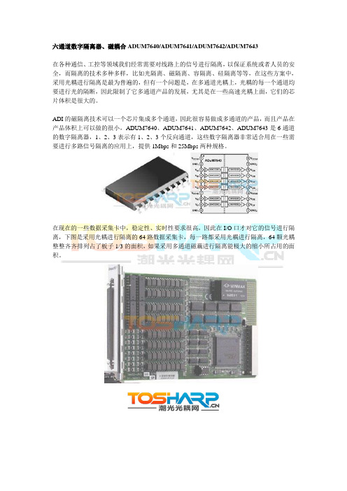
六通道数字隔离器、磁耦合ADUM7640/ADUM7641/ADUM7642/ADUM7643
在各种通信、工控等领域我们经常需要对线路上的信号进行隔离,以保证系统或者人员的安全,而隔离的技术多种多样,比如光隔离、磁隔离、容隔离、硅隔离等等,在这些方案中,采用光耦进行隔离是最为普遍的,但有一个问题是,在多通道光耦上,光耦的每一个通道均要进行光的隔断,因此限制了它多通道产品的发展,尤其是在一些高速光耦上面,它们的芯片体积是很大的。
ADI的磁隔离技术可以一个芯片集成多个通道,因此很容易做成多通道的产品,而且产品在产品体积上可以做的很小,ADUM7640、ADUM7641、ADUM7642、ADUM7643是6通道的数字隔离器,1、2、3表示有1、2、3个反向通道,这些数字隔离器非常适合用在一些需要进行多路信号隔离的应用上,提供1Mbps和25Mbps两种规格。
在现在的一些数据采集卡中,稳定性、实时性要求很高,因此在I/O口才对它的信号进行隔离,下图是采用光耦进行隔离的64路数据采集卡,每一路都采用光耦进行隔离,64颗光耦整整齐齐排列占了板子1/3的面积,如果采用多通道磁藕进行隔离能极大的缩小所占用的面积。
双通道数字隔离芯片_解释说明

双通道数字隔离芯片解释说明1. 引言1.1 概述双通道数字隔离芯片是一种重要的电子元件,用于解决电路信号隔离和保护的问题。
它能够将输入信号和输出信号之间实现高度可靠的电气隔离,防止输入端的干扰信号传播到输出端,并保证数据的安全性。
这种芯片在现代电子设备中应用广泛,从工业自动化系统到医疗仪器等领域都有其身影。
1.2 文章结构本文将对双通道数字隔离芯片进行详细介绍和分析。
首先,在引言部分我们将给出该文章的结构,包括各个章节内容简介和组织框架。
接下来,第二节将对双通道数字隔离芯片的定义、原理和工作原理进行解释说明。
在第三节中,我们将重点讨论第一通道相关要点,包括数字隔离技术介绍、设计要求以及实现方式和性能评估。
然后在第四节,我们将深入探讨第二通道相关要点,同样包括技术介绍、设计要求以及实现方式和性能评估。
最后,在结论部分我们将总结主要观点,并提出未来研究方向。
1.3 目的本文的目的是为读者提供关于双通道数字隔离芯片的全面了解。
我们将对该芯片的原理、工作方式以及在不同应用领域中的重要性进行解释和阐述。
通过详细探讨第一通道和第二通道,读者将能够更好地理解双通道数字隔离芯片的设计要求和实现方式,并深入了解其性能评估方法。
最后,我们希望通过总结观点并提出未来研究方向,促进该领域的发展与创新。
2. 双通道数字隔离芯片2.1 定义和原理双通道数字隔离芯片是一种电子元件,用于在不同电路之间提供高度可靠的电气隔离。
它基于数字隔离技术,通过光耦合器、磁耦合器或者互感器等方式,将输入信号与输出信号之间实现完全的电气隔离。
该芯片的原理是利用特殊材料和工艺,在芯片内部划分出两个独立的电路区域,并以某种方式引入物理屏障。
这样可以避免因输入端与输出端直接相连而可能引发的干扰、噪声或者潜在的安全风险。
2.2 工作原理双通道数字隔离芯片通过将输入信号转换成光、磁或者电压等形式进行传输,并在输出端将其重新转换回原有形式,使得输入信号与输出信号之间无任何导电连接。
模拟信号的隔离方法有哪些

模拟信号的隔离方法有哪些隔离数字信号的办法很多,隔离模拟信号的办法却没有想象的那么多,关键是隔离的成本,比想象的都要高出许多。
特别是要求精确测量的场合,模拟信号的隔离,成本高得更加是离谱的无法想象。
我从事这种系统开发多年,对自己所知道的隔离方法做个小小的总结:数字隔离方法:1. 光耦;2. ADI 的磁隔离芯片,ADuMXXXX(XXXX为数字代号,如 I2C的ADuM1250);3.自己用变压器隔离。
数字隔离办法,一般实现的都是单向数字信号的隔离,对于双向数字信号,需要两个隔离单元来实现,体积非常的惊人;很难减小体积。
相对于速度很成本,如果速度小于100KHz一下,个人推荐用Ps2501这样的常用光耦隔离数字信号,很好的性价比,隔离度也非常的高。
一般Ps2501这样的光耦隔离度都在3000V/RMS以上。
但是如果隔离数字信号的频率在200KHz以上,用Ps2501这样的光耦就不行了,要换高速的数字光耦,价格成本也上去了,不划算了。
所以可采用ADI的磁隔离芯片。
最便宜的磁隔离芯片每通道的价格在$0.7,算下来人民币也才4~5块人民币,选在6N137、6N136这样的高速光耦,已经没有性价比可言,浪费大量的PCB空间用于隔离部分。
成本在4块左右,甚至更高,主要看你的6N137的采购量。
但ADuM系列的磁隔离芯片的尺寸小很多很多,价格相比也很有优势。
唯一美中不足的是磁隔离芯片的隔离电压只能到1000V左右,这个是个很头疼的问题。
如果只是隔离干扰源,自然没问题,如果是隔离高电压,那么要仔细考量一下设计了。
自己用隔离变压器来隔离的办法,一般人是用不到的,因为完全没有经济效益。
它只有一点好处,就是隔离电压可做得非常高,一般只有变频器、逆变器等IGBT的驱动,需要隔离非常大的电压,超过5000V;才使用。
因为一般的芯片和光耦都实现不了了。
模拟信号的隔离:1.线性光耦;2. 隔离放大器 ;3.频压转换和压频转换+数字隔离;4.飞电容;5.采用DA/AD+数字隔离的办法实现模拟信号的采样复原,进而实现隔离的办法;6.普通光耦实现的线性隔离。
- 1、下载文档前请自行甄别文档内容的完整性,平台不提供额外的编辑、内容补充、找答案等附加服务。
- 2、"仅部分预览"的文档,不可在线预览部分如存在完整性等问题,可反馈申请退款(可完整预览的文档不适用该条件!)。
- 3、如文档侵犯您的权益,请联系客服反馈,我们会尽快为您处理(人工客服工作时间:9:00-18:30)。
Isolated High-Speed CAN Transceiver Functional DiagramTxD RxDCANHCANLIL41050SV DD2 (V) TxD(1)S CANH CANL BusState RxD 4.75 to 5.25 ↓ Low(2) High Low Dominant Low 4.75 to 5.25 X High V DD2/2 V DD2/2 Recessive High 4.75 to 5.25 ↑ XV DD2/2 V DD2/2 Recessive High<2V (no pwr) X X 0<V<2.5 0<V<2.5 Recessive High 2>V DD2<4.75 >2V X 0<V<2.5 0<V<2.5 Recessive High Table 1. Function table.Notes:1. TxD input is edge triggered: ↑ = Logic Lo to Hi, ↓ = Hi to Lo2. Valid for logic state as described or open circuitX = don’t care. Features• Single-chip isolated CAN/DeviceNet transceiver• Fully compliant with the ISO 11898 CAN standard• Best-in-class loop delay (180 ns)• 3.0 V to 5.5 V input power supplies• >110-node fan-out• High speed (up to 1 Mbps)• 2,500 V RMS isolation (1 minute)• Very low Electromagnetic Emission (EME)• Differential signaling for excellent Electromagnetic Immunity (EMI)• 30 kV/µs transient immunity• Silent mode to disable transmitter• Unpowered nodes do not disturb the bus• Transmit data (TxD) dominant time-out function• Edge triggered, non-volatile input improves noise performance • Bus pin transient protection for automotive environment• Thermal shutdown protection• Short-circuit protection for ground and bus power• −55°C to +125°C operating temperature• JEDEC-standard 16-pin SOIC package• UL1577 and IEC 61010-2001 approvedApplications• Noise-critical CAN• Partially-powered CAN• DeviceNet• Factory automationDescriptionThe IL41050 is a galvanically isolated, high-speed CAN (Controller Area Network) transceiver, designed as the interface between the CAN protocol controller and the physical bus. The IL41050 provides isolated differential transmit capability to the bus and isolated differential receive capability to the CAN controller via NVE’s patented* IsoLoop spintronic Giant Magnetoresistance (GMR) technology.Advanced features facilitate reliable bus operation. Unpowered nodes do not disturb the bus, and a unique non-volatile programmable power-up feature prevents unstable nodes. The devices also have a hardware-selectable silent mode that disables the transmitter. Designed for harsh CAN and DeviceNet environments, IL41050T transceivers have transmit data dominant time-out, bus pin transient protection, thermal shutdown protection, and short-circuit protection, Unique edge-triggered inputs improve noise performance. Unlike optocouplers or other isolation technologies, IsoLoop isolators have indefinite life at high voltage.IsoLoop® is a registered trademark of NVE Corporation. REV. CAbsolute Maximum Ratings (1) (2)ParametersSymbol Min. Typ. Max. Units Test Conditions Storage temperatureT S −55 150 °C Ambient operating temperatureT A −40 135 °CDC voltage at CANH and CANL pins V CANH V CANL −27 40 V0 V< V DD2 < 5.25 V;indefinite durationSupply voltageV DD 1 , V DD 2 −0.5 6 V Digital input voltage V TxD , V S −0.3 V DD + 0.3 V Digital output voltage V RxD −0.3 V DD + 0.3 V DC voltage at V REFV REF −0.3 V DD + 0.3 V Transient Voltage at CANH or CANL V trt(CAN) −200 200 V Electrostatic discharge at all pins V esd −4,000 4,000 V Human body model Electrostatic discharge at all pinsV esd −200 200 V Machine modelRecommended Operating ConditionsParameters Symbol Min. Typ. Max. Units Test ConditionsSupply voltageV DD 1 V DD 2 3.0 4.75 5.55.25 VInput voltage at any bus terminal (separately or common mode) V CANHV CANL−12 12 VHigh-level digital input voltage (3) (4) V IH 2.0 2.4 2.0 V DD 1V DD 1V DD 2 V V DD 1 = 3.3 V V DD 1 = 5.0 V V DD 2 = 5.0 VLow-level digital input voltage (3) (4) V IL 0 0.8 V Digital output current (RxD) I OH −8 8 mA V DD1 = 3.3V to 5V Ambient operating temperatureT A −40 125 °C Digital input signal rise and fall timest IR , t IF 1 μsInsulation SpecificationsParametersSymbol Min. Typ. Max. Units Test ConditionsCreepage distance (external)8.08 mmBarrier impedance > 1014|| 7 Ω || pF Leakage current0.2 μA RMS 240 V RMS , 60 HzSafety and ApprovalsIEC61010-2001TUV Certificate Numbers:N1502812 (pending)Classification: Reinforced InsulationModelPackage Pollution Degree Material Group Max. Working VoltageIL41050SOIC (0.3")II III 300 V RMSUL 1577Component Recognition Program File Number: E207481 (pending) Rated 2,500V RMS for 1 minuteSoldering ProfilePer JEDEC J-STD-020CMoisture Sensitivity Level: MSL=2Notes:1. Absolute Maximum specifications mean the device will not be damaged if operated under these conditions. It does not guarantee performance.2. All voltages are with respect to network ground except differential I/O bus voltages.3. The TxD input is edge sensitive. Voltage magnitude of the input signal is specified, but edge rate specifications must also be met.4. The maximum time allowed for a logic transition at the TxD input is 1 μs.Pin Connections1 V DD1 V DD1 power supply input2 GND1 V DD1 power supply ground return (pin 2 is internally connected to pin 8)3 TxD Transmit Data input4 NCNo internal connection5 RxD Receive Data output6 NC No internal connection7 NC No internal connection8 GND1 V DD1 power supply ground return (pin 8 is internally connected to pin 2)9 GND2 V DD2 power supply ground return (pin 9 is internally connected to pin 15)10 V REF Reference voltage output11 V DD2 V DD2 power supply input12 CANL Low level CANbus line13 CANH High level CANbus line14 S Mode select input (high speed/silent select)15 GND2 V DD2 power supply ground return (pin 15 is internally connected to pin 9)16 V DD2 V DD2 power supply inputNCVDD2GND1NCGND2SCANH RxD CANLV REFGND1VDD1GND2 TxDNCVDD2SpecificationsSpecifications (...cont.)Electrical Specifications are T min to T max and V DD1, V DD2= 4.5 V to 5.5 V unless otherwise stated.Differential input capacitance C i(dif) 3.7510 pFV TxD = V DD1Input leakage current at CANH I LI(CANH) 100 170 250 μA V CANH= 5 V, V DD2= 0 V Input leakage current at CANL I LI(CANL) 100 170 250 μA V CANL= 5 V, V DD2= 0 V Thermal ShutdownShutdown junction temperature T j(SD) 155 165 180 °CTiming CharacteristicsTxD to bus active delay t d(TxD-BUSon)29326366125128nsV S= 0 V; V DD1 = 5 VV S = 0 V; V DD1 = 3.3 VTxD to bus inactive delay t d(TxD-BUSoff)29326871110113nsV S = 0 V; V DD1 = 5 VV S = 0 V; V DD1 = 3.3 VBus active to RxD delay t d(BUSon-RxD)24275861125128nsV S = 0 V; V DD1 = 5 VV S = 0 V; V DD1 = 3.3 VBus inactive to RxD delay t d(BUSoff-RxD)4952103106170173nsV S = 0 V; V DD1 = 5 VV S = 0 V; V DD1 = 3.3 VTxD dominant time for timeout T dom(TxD) 250 457 765 μs V TxD = 0 V3.0 V > V DD1 < 5.5 VMagnetic Field Immunity(3)V DD1 = 5 V, V DD2 = 5 VPower frequency magnetic immunity H PF2,500 3,000 A/m 50 Hz/60 HzPulse magnetic field immunity H PM 3,000 3,500 A/m t p = 8 µsCross-axis immunity multiplier K X 1.8 Figure1V DD1 = 3.3 V, V DD2 = 5 VPower frequency magnetic immunity H PF1,000 1,500 A/m 50 Hz/60 HzPulse magnetic field immunity H PM 1,800 2,000 A/m t p = 8 µsCross-axis immunity multiplier K X 1.5 Figure1 Notes:1. The TxD input is edge sensitive. Voltage magnitude of the input signal is specified, but edge rate specifications must also be met.2. The maximum time allowed for a logic transition at the TxD input is 1 μs.3. Uniform magnetic field applied across the pins of the device. Cross-axis multiplier effective when field is applied perpendicular to the pins. Electrostatic Discharge SensitivityThis product has been tested for electrostatic sensitivity to the limits stated in the specifications. However, NVE recommends that all integrated circuits be handled with appropriate care to avoid damage. Damage caused by inappropriate handling or storage could range from performance degradation to complete failure.Electromagnetic CompatibilityThe IL41050 is fully compliant with generic EMC standards EN50081, EN50082-1 and the umbrella line-voltage standard for Information Technology Equipment (ITE) EN61000. The IsoLoop Isolator’s Wheatstone bridge configuration and differential magnetic field signaling ensure excellent EMC performance against all relevant standards. NVE conducted compliance tests in the categories below:EN50081-1Residential, Commercial & Light IndustrialMethods EN55022, EN55014EN50082-2: Industrial EnvironmentMethods EN61000-4-2 (ESD), EN61000-4-3 (Electromagnetic Field Immunity), EN61000-4-4 (Electrical Transient Immunity),EN61000-4-6 (RFI Immunity), EN61000-4-8 (Power Frequency Magnetic Field Immunity), EN61000-4-9 (Pulsed MagneticField), EN61000-4-10 (Damped Oscillatory Magnetic Field)ENV50204Radiated Field from Digital Telephones (Immunity Test)Immunity to external magnetic fields is higher if the field direction is “end-to-end” (rather than to “pin-to-pin”) as shown in thediagram at right. Fig. 1Application InformationPower Supply DecouplingBoth V DD1 and V DD2 must be bypassed with 100 nF ceramic capacitors. These supply the dynamic current required for the isolator switching and should be placed as close as possible to V DD and their respective ground return pins.Dominant Mode Time-out and Failsafe Receiver FunctionsCAN bus latch up is prevented by an integrated Dominant mode timeout function. If the TxD pin is forced permanently low by hardware or software application failure, the time-out returns the TxD output to the high state no more than 765 μs after TxD is asserted dominant. The timer is triggered by a negative edge on TxD. If the duration of the low is longer than the internal timer value, the transmitter is disabled, driving the bus to the recessive state. The timer is reset by a positive edge on pin TxD.If power is lost on Vdd2, the IL41050 asserts the RxD output high when the supply voltage falls below 3.8 V. RxD will return to normal operation as soon as Vdd2 rises above approximately 4.2 V.The Isolation AdvantageBattery fire caused by over or under charging of individual lithium ion cells is a major concern in multi-cell high voltage electric and hybrid vehicle batteries. To combat this, each cell is monitored for current flow, cell voltage, and in some advanced batteries, magnetic susceptibility. The IL41050 allows seamless connection of the monitoring electronics of every cell to a common CAN bus by electrically isolating inputs from outputs, effectively isolating each cell from all other cells. Cell status is then monitored via the CAN controller in the Battery Management System (BMS).Another major advantage of isolation is the tremendous increase in noise immunity it affords the CAN node, even if the power source is a battery. Inductive drives and inverters can produce transient swings in excess of 20 kV/μs. The traditional, non-isolated CAN node provides some protection due to differential signaling and symmetrical driver/receiver pairs, but the IL41050 typically provides more than twice the dV/dt protection of a traditional CAN node.SJA1000IL41050Fig. 2. Isolated CAN node using the IL41050 and an SJA1000 MCU.Programmable Power-UpA unique non-volatile programmable power-up feature prevents unstable nodes. A state that needs to be present at node power up can be programmed at the last power down. For example if a CAN node is required to “pulse” dominant at power up, TxD can be sent low by the controller immediately prior to power down. When power is resumed, the node will immediately go dominant allowing self-check code in the microcontroller to verify node operation. If desired, the node can also power up silently by presetting the TxD line high at power down. At the next power on, the IL41050 will remain silent, awaiting a dominant state from the bus.The microcontroller can check that the CAN node powered down correctly before applying power at the next “power on” request. If the node powered down as intended, RxD will be set high and stored in IL41050’s non-volatile memory. The level stored in the RxD bit can be read before isolated node power is enabled, avoiding possible CAN bus disruption due to an unstable node.Package Drawings, Dimensions and SpecificationsOrdering Information and Valid Part NumbersBulk Packaging Blank = TubeTR13 = 13'' Tape and Reel PackageE = RoHS Compliant Temperature RangeT = Extended (-55˚C to +125˚C)Channel Configuration 1050 = CAN Transceiver Base Part Number4 = Isolated Transceiver Product Family IL = IsolatorsValid Part Numbers IL41050TEIL4150TE TR13RoHSCOMPLIANTRevision HistoryISB-DS-001-IL41050-C February 2010 Changes• Min. operating temperature changed to −55°C • Misc. changes and clarifications for final release.ISB-DS-001-IL41050-B January 2010 Change• Clarified TxD edge trigger mode. Added information to Applications section. Tightened timing specifications.ISB-DS-001-IL41050-A January 2010 Change• Initial release.About NVEAn ISO 9001 Certified CompanyNVE Corporation manufactures innovative products based on unique spintronic Giant Magnetoresistive (GMR) technology. Products include Magnetic Field Sensors, Magnetic Field Gradient Sensors (Gradiometers), Digital Magnetic Field Sensors, Digital Signal Isolators, and Isolated Bus Transceivers.NVE pioneered spintronics and in 1994 introduced the world’s first products using GMR material, a line of ultra-precise magnetic sensors for position, magnetic media, gear speed and current sensing.NVE Corporation11409 Valley View RoadEden Prairie, MN 55344-3617 USATelephone: (952) 829-9217Fax: (952) 829-9189Internet: e-mail: isoinfo@The information provided by NVE Corporation is believed to be accurate. However, no responsibility is assumed by NVE Corporation for its use, nor for any infringement of patents, nor rights or licenses granted to third parties, which may result from its use. No license is granted by implication, or otherwise, under any patent or patent rights of NVE Corporation. NVE Corporation does not authorize, nor warrant, any NVE Corporation product for use in life support devices or systems or other critical applications, without the express written approval of the President of NVE Corporation.Specifications are subject to change without notice.ISB-DS-001-IL41050-CFebruary 2010。