MC100LVEL11DTG;MC100LVEL11DR2G;MC100LVEL11DTR2G;MC100LVEL11MNR4G;中文规格书,Datasheet资料
MC100ELT23D中文资料
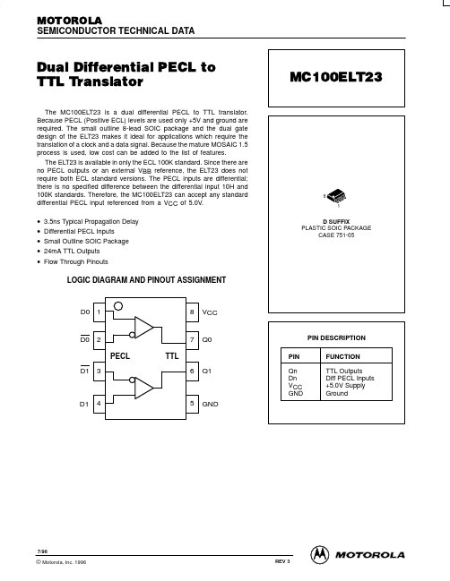
LOGIC DIAGRAM AND PINOUT ASSIGNMENT
D0 1
8
VCC
D0
2 PECL TTL
7
Q0
PIN
PIN DESCRIPTION FUNCTION TTL Outputs Diff PECL Inputs +5.0V Supply Ground
D1
3
6
Q1
Qn Dn VCC GND
* Maximum Ratings are those values beyond which damage to the device may occur. Functional operation should be restricted to the Recommended Operating Conditions.
1. 200mV input guarantees full logic swing at the output.
AC CHARACTERISTICS (VCC = 4.75V to 5.25V; TA = –40°C to 85°C)
–40°C Symbol tPLH tPHL Characteristic Propagation Delay1 Propagation Delay1 Min 2.0 2.0 Max 52.0 2.0 25°C Typ Max 5.5 5.5 85°C Min 2.0 2.0 Max 5.5 5.5 Unit ns ns Condition CL = 20pF CL = 20pF
MOTOROLA
3–2
ECLinPS and ECLinPS Lite DL140 — Rev 3
元器件交易网
MC100ELT23
88E1116R_Technical_Product_Brief
Marvell.Moving Forward FasterDoc. No. MV-S105539-00, Rev. --May 9, 2011Document Classification: Proprietary InformationAlaska ® 88E1116RTechnical Product BriefGigabit Ethernet TransceiverAlaska® 88E1116R Technical Product BriefGigabit Ethernet TransceiverDocument ConventionsNote: Provides related information or information of special importance.Caution: Indicates potential damage to hardware or software, or loss of data.Warning: Indicates a risk of personal injury.Document StatusDoc Status: Advance Technical Publications: 1.00For more information, visit our website at: DisclaimerNo part of this document may be reproduced or transmitted in any form or by any means, electronic or mechanical, including photocopying and recording, for any purpose, without the express written permission of Marvell. Marvell retains the right to make changes to this document at any time, without notice. Marvell makes no warranty of any kind, expressed or implied, with regard to any information contained in this document, including, but not limited to, the implied warranties of merchantability or fitness for any particular purpose. Further, Marvell does not warrant the accuracy or completeness of the information, text, graphics, or other items contained within this document.Marvell products are not designed for use in life-support equipment or applications that would cause a life-threatening situation if any such products failed. Do not use Marvell products in these types of equipment or applications.With respect to the products described herein, the user or recipient, in the absence of appropriate U.S. government authorization, agrees:1) Not to re-export or release any such information consisting of technology, software or source code controlled for national security reasons by the U.S. Export Control Regulations ("EAR"), to a national of EAR Country Groups D:1 or E:2;2) Not to export the direct product of such technology or such software, to EAR Country Groups D:1 or E:2, if such technology or software and direct products thereof are controlled for national security reasons by the EAR; and,3) In the case of technology controlled for national security reasons under the EAR where the direct product of the technology is a complete plant or component of a plant,not to export to EAR Country Groups D:1 or E:2 the direct product of the plant or major component thereof, if such direct product is controlled for national security reasonsby the EAR, or is subject to controls under the U.S. Munitions List ("USML").At all times hereunder, the recipient of any such information agrees that they shall be deemed to have manually signed this document in connection with their receipt of any such information.Copyright © 1999–2011. Marvell International Ltd. All rights reserved. Marvell, Moving Forward Faster, the Marvell logo, Alaska, AnyVoltage, DSP Switcher, Fastwriter, Feroceon, Libertas, Link Street, PHYAdvantage, Prestera, TopDog, Virtual Cable Tester, Yukon, and ZJ are registered trademarks of Marvell or its affiliates. CarrierSpan, LinkCrypt, Powered by Marvell Green PFC, Qdeo, QuietVideo, Sheeva, TwinD, and VCT are trademarks of Marvell or its affiliates.Patent(s) Pending—Products identified in this document may be covered by one or more Marvell patents and/or patent applications.Doc. No. MV-S105539-00 Rev. -- Copyright © 2011 Marvell Page 2Document Classification: Proprietary Information May 9, 2011, AdvanceAlaska ® 88E1116R Technical Product BriefGigabit Ethernet TransceiverCopyright © 2011 Marvell Doc. No. MV-S105539-00, Rev. --May 9, 2011, AdvanceDocument Classification: Proprietary InformationPage 3O VERVIEWThe Alaska ® 88E1116R Gigabit Ethernet Transceiver is a physical layer device containing a single Gigabit Ethernet transceiver. The transceiver implements the Ethernet physical layer portion of the 1000BASE-T, 100BASE-TX, and 10BASE-T standards. It is manu-factured using standard digital CMOS process and contains all the active circuitry required to implement the physical layer functions to transmit and receive data on standard CAT 5 unshielded twisted pair.The 88E1116R device supports the RGMII (Reduced pin count GMII) for direct connection to a MAC/Switch port.The 88E1116R device integrates MDI interface termi-nation resistors into the PHY . This resistor integration simplifies board layout and reduces board cost by reducing the number of external components. The new Marvell ® calibrated resistor scheme will achieve and exceed the accuracy requirements of the IEEE 802.3 return loss specifications.The 88E1116R device can run off a single 1.8V, 2.5V, or 3.3V supply. Alternatively if the regulators are not used then the 88E1116R device can run off 1.8V and1.2V supply.The 88E1116R device has two regulators to generate all required voltages. The 88E1116R device supports 1.8V, 2.5V, and 3.3V HSTL/SSTL and 2.5V LVCMOS I/O StandardsThe 88E1116R device incorporates the Marvell® Vir-tual Cable Tester ® (VCT™) feature, which uses Time Domain Reflectometry (TDR) technology for the remote identification of potential cable malfunctions, thus reducing equipment returns and service calls. Using VCT, the Alaska 88E1116R device detects and reports potential cabling issues such as pair swaps, pair polarity and excessive pair skew. The device will also detect cable opens, shorts or any impedance mis-match in the cable and reporting accurately within one meter the distance to the fault.The 88E1116R device uses advanced mixed-signal processing to perform equalization, echo and crosstalkcancellation, data recovery, and error correction at a gigabit per second data rate. The device achieves robust performance in noisy environments with very low power dissipation.F EATURES•10/100/1000BASE-T IEEE 802.3 compliant •Four RGMII timing modes - This eliminates the need for adding trace delays on the PCB•Supports LVCMOS, SSTL, and HSTL I/O Stan-dards on the RGMII interface•Integrated MDI interface termination resistors that eliminate twelve passive components•Energy Detect and Energy Detect+ low power modes•Three loopback modes for diagnostics•“Downshift” mode for two-pair cable installations •Fully integrated digital adaptive equalizers, echo cancellers, and crosstalk cancellers•Advanced digital baseline wander correction •Automatic MDI/MDIX crossover at all speeds of operation•Automatic polarity correction•IEEE 802.3u compliant Auto-Negotiation•Software programmable LED modes including LED testing•Supports IEEE 1149.1 JTAG•MDC/MDIO Management Interface •CRC checker, packet counter •Packet generation•Virtual Cable Tester (VCT)•Auto-Calibration for MAC Interface outputs •Coma Mode support•Requires a single 1.8V supply•I/O pads can be supplied with 1.8V, 2.5V, or 3.3V •Two regulators generate all required voltages. Regulator can be supplied with 1.8V, 2.5V or 3.3V.•Commercial grade •64-Pin QFN package88E1116R Device used in Copper ApplicationAlaska ® 88E1116R Technical Product BriefGigabit Ethernet TransceiverDoc. No. MV-S105539-00, Rev. -- Copyright © 2011 MarvellPage 4Document Classification: Proprietary InformationMay 9, 2011, AdvanceTable of ContentsS ECTION 1.S IGNAL D ESCRIPTION (5)1.1Pin Description...............................................................................................................61.1.1Pin Type Definitions (6)1.264-Pin QFN Pin Assignment List - Alphabetical by Signal Name (13)S ECTION 2.P ACKAGE M ECHANICAL D IMENSIONS (14)2.164-Pin QFN Package (14)Copyright © 2011 Marvell Doc. No. MV-S105539-00, Rev. --May 9, 2011, AdvanceDocument Classification: Proprietary InformationPage 5Signal DescriptionSection 1. Signal DescriptionThe 88E1116R device is a 10/100/1000BASE-T Gigabit Ethernet transceiver.Figure 1:88E1116R Device 64-Pin QFN Package (Top View)34567891011121314Top ViewC O N F I G [3]C O M A n L ED [0]V D D OL E D [1]L E D [2]R E S E T nA V D D RD V D DD I S _RE G 12D V D D88E1116RT R S T nAlaska ®88E1116R Technical Product Brief Gigabit Ethernet TransceiverDoc. No. MV-S105539-00, Rev. -- Copyright © 2011 Marvell Page 6Document Classification: Proprietary InformationMay 9, 2011, Advance1.1Pin Description1.1.1Pin Type DefinitionsPin TypeDefinitionH Input with hysteresis I/O Input and output I Input only O Output only PU Internal pull up PD Internal pull down D Open drain output Z Tri-state output mADC sink capabilityCopyright © 2011 Marvell Doc. No. MV-S105539-00, Rev. --May 9, 2011, AdvanceDocument Classification: Proprietary InformationPage 7Signal DescriptionPin DescriptionTable 1:Media Dependent Interface 64-QFN Pin #Pin NamePin TypeDescription3031MDIN[0]MDIP[0]I/O, DMedia Dependent Interface[0].In 1000BASE-T mode in MDI configuration, MDIN/P[0] correspond to BI_DA±. In MDIX configuration, MDIN/P[0] correspond to BI_DB±.In 100BASE-TX and 10BASE-T modes in MDI configuration, MDIN/P[0] are used for the transmit pair. In MDIX configuration, MDIN/P[0] are used for the receive pair.“The unused MDI pins cannot be connected to ground. They need to be left floating, because they have internal bias.The 88E1116R device contains an internal 100 ohm resistor between the MDIP/N[0] pins.2526MDIN[1]MDIP[1]I/O, D Media Dependent Interface[1].In 1000BASE-T mode in MDI configuration, MDIN/P[1] correspond to BI_DB±. In MDIX configuration, MDIN/P[1] correspond to BI_DA±.In 100BASE-TX and 10BASE-T modes in MDI configuration, MDIN/P[1] are used for the receive pair. In MDIX configuration, MDIN/P[1] are used for the transmit pair.“The unused MDI pins cannot be connected to ground. They need to be left floating, because they have internal bias.The 88E1116R device contains an internal 100 ohm resistor between the MDIP/N[0] pins.2324MDIN[2]MDIP[2]I/O, D Media Dependent Interface[2].In 1000BASE-T mode in MDI configuration, MDIN/P[2] correspond to BI_DC±. In MDIX configuration, MDIN/P[2] corresponds to BI_DD±. In 100BASE-TX and 10BASE-T modes, MDIN/P[2] are not used.“The unused MDI pins cannot be connected to ground. They need to be left floating, because they have internal bias.The 88E1116R device contains an internal 100 ohm resistor between the MDIP/N[0] pins.1920MDIN[3]MDIP[3]I/O, D Media Dependent Interface[3].In 1000BASE-T mode in MDI configuration, MDIN/P[3] correspond to BI_DD±. In MDIX configuration, MDIN/P[3] correspond to BI_DC±.In 100BASE-TX and 10BASE-T modes, MDIN/P[3] are not used.“The unused MDI pins cannot be connected to ground. They need to be left floating, because they have internal bias.The 88E1116R device contains an internal 100 ohm resistor between the MDIP/N[0] pins.Alaska ® 88E1116R Technical Product BriefGigabit Ethernet TransceiverDoc. No. MV-S105539-00, Rev. -- Copyright © 2011 Marvell Page 8Document Classification: Proprietary InformationMay 9, 2011, AdvanceThe RGMII interface supports 10/100/1000BASE-T mode of operation.Table 2:RGMII Interface 64-QFN Pin #Pin NamePin TypeDescription60TX_CLK I RGMII Transmit Clock provides a 125 MHz, 25 MHz, or 2.5 MHz reference clock with ± 50 ppm tolerance depending on speed.63TX_CTRLIRGMII Transmit Control. TX_EN is presented on the rising edge of TX_CLK. A logical derivative of TX_EN and TX_ER is presented on the falling edge of TX_CLK.62615958TXD[3]TXD[2]TXD[1]TXD[0]IRGMII Transmit Data.TXD[3:0] run at double data rate with bits [3:0] presented on the rising edge of TX_CLK, and bits [7:4] presented on the falling edge of TX_CLK.In 10/100BASE-T modes, the transmit data nibble is presented on TXD[3:0] on the rising edge of TX_CLK.53RX_CLK ORGMII Receive Clock provides a 125 MHz, 25 MHz, or 2.5 MHz reference clock with ± 50 ppm tolerance derived from the received data stream depending on speed.49RX_CTRL ORGMII Receive Control. RX_DV is presented on the rising edge of RX_CLK.A logical derivative of RX_DV and RX_ER is presented on the falling edge of RX_CLK.55545150RXD[3]RXD[2]RXD[1]RXD[0]ORGMII Receive Data. RXD[3:0] run at double data rate with bits [3:0] presented on the rising edge of RX_CLK, and bits [7:4] presented on the falling edge of RX_CLK.In 10/100BASE-T modes, the receive data nibble is presented on RXD[3:0] on the rising edge of RX_CLK.Copyright © 2011 Marvell Doc. No. MV-S105539-00, Rev. --May 9, 2011, AdvanceDocument Classification: Proprietary InformationPage 9Signal DescriptionPin DescriptionTable 3:Management Interface and Interrupt 64-QFN Pin #Pin NamePin TypeDescription48MDCIMDC is the management data clock reference for the serial management interface. A continuous clock stream is not expected. The maximum fre-quency supported is 8.3 MHz.45MDIO I/OMDIO is the management data. MDIO transfers management data in and out of the device synchronously to MDC. This pin requires a pull-up resistor in a range from 1.5 kohm to 10 kohm.Table 4:LED Interface 64-QFN Pin #Pin NamePin TypeDescription689LED[0]LED[1]LED[2]OLED/Interrupt outputs.Table 5:JTAG Interface 64-QFN Pin #Pin NamePin TypeDescription43TDI I Boundary scan test data input.41TMS I, PU Boundary scan test mode select input.TMS contains an internal 150 kohm pull-up resistor. 42TCK I, PU Boundary scan test clock input.TCK contains an internal 150 kohm pull-up resistor.11TRSTnI, PUBoundary scan test reset input. Active low. TRSTn contains an internal 150 kohm pull-up resistor as per the 1149.1 specification. After power up, the JTAG state machine should be reset by applying a low signal on this pin, or by keeping TMS high and applying 5 TCK pulses, or by pulling this pin low by a 4.7 kohm resistor.44TDO OBoundary scan test data output.Alaska ® 88E1116R Technical Product BriefGigabit Ethernet TransceiverDoc. No. MV-S105539-00, Rev. -- Copyright © 2011 Marvell Page 10Document Classification: Proprietary InformationMay 9, 2011, AdvanceTable 6:Clock/Configuration/Reset/I/O 64-QFN Pin #Pin NamePin TypeDescription64CONFIG[0]I Hardware Configuration 1CONFIG[1]I Hardware Configuration 2CONFIG[2]I Hardware Configuration 3CONFIG[3]I Hardware Configuration38XTAL_INIReference Clock. 25 MHz ± 50 ppm tolerance crystal reference or oscillator input.NOTE: If AVDDC is tied to 1.8V, then the XTAL_IN pin is not 2.5V/3.3V tolerant.If AVDDC is tied to 2.5V, then the XTAL_IN pin is not 3.3V tolerant.39XTAL_OUT 0Reference Clock. 25 MHz ± 50 ppm tolerance crystal reference. When the XTAL_OUT pin is not connected, it should be left floating.10RESETnIHardware reset. Active low.0 = Reset 1 = Normal57VREF IRGMII input voltage reference.Must be set to VDDOR/2 when used as 1.8V HSTL, 2.5V SSTL_2, and 3.3V. Set to VDDOR when used as 2.5V LV CMOS.Copyright © 2011 Marvell Doc. No. MV-S105539-00, Rev. --May 9, 2011, AdvanceDocument Classification: Proprietary InformationPage 11Signal DescriptionPin DescriptionTable 7:Test 64-QFN Pin #Pin NamePin TypeDescription3536HSDACN HSDACPO OAC Test Point. Positive and Negative.These pins are also used to bring out a differential TX_TCLK. Connect these pins with a 50 ohm termination resistor to VSS for IEEE testing and debug purposes. If debug and IEEE testing are not of importance, these pins can be left floating.32TSTPT OTest Point.Table 8:Control and Reference 64-QFN Pin #Pin NamePin TypeDescription33RSET I Constant voltage reference. External 4.99 kohm 1% resistor connection to VSS required for each pin.17CTRL18O 1.8V Regulator Control. This signal ties to the base of the BJT. If the 1.8V regulator is not used it can be left floating.12DIS_REG12I1.2V Regulator Disable. Tie to VDDO to disable, tie to VSS to enable.Alaska ® 88E1116R Technical Product BriefGigabit Ethernet TransceiverDoc. No. MV-S105539-00, Rev. -- Copyright © 2011 Marvell Page 12Document Classification: Proprietary InformationMay 9, 2011, AdvanceTable 9:Power & Ground 64-QFN Pin #Pin NamePin TypeDescription21222729AVDDPowerAnalog supply. 1.8V 1. AVDD can be supplied externally with 1.8V, or via the 1.8V regulator.1. AVDD supplies the MDIP/N[3:0] pins.3437AVDDCAnalog supply - 1.8V or 2.5V, or 3.3V 2.AVDDC must be supplied externally. Do not use the 1.8V regulator to power AVDDC.2. AVDDC supplies the XTAL_IN and XTAL_OUT pins.1415AVDDR1.2V Regulator supply - 1.8VAVDDR can be supplied externally with 1.8V, or via the 1.8V regulator. If the 1.2V regulator is not used, AVDDR must still be tied to 1.8V.16AVDDXPower1.8V Regulator supply -2.5V,3.3V, (or 1.8V).AVDDX must be supplied externally. Note that this supply must be the same voltage as AVDDC.If the 1.8V regulator is not used, then it means a 1.8V supply is in the sys-tem. AVDDX (along with AVDDC) would be tied to 1.8V in this case.5134047DVDD PowerDigital core supply - 1.2V.DVDD can be supplied externally with 1.2V, or via the 1.2V regulator.746VDDO Power1.8V,2.5V, or3.3V non-RGMII digital I/O supply 3.VDDO must be supplied externally. Do not use the 1.8V regulator to power VDDO.3. VDDO supplies the MDC, MDIO, RESETn, LED[2:0], CONFIG[3:0], TDI, TMS, TCK, TRSTn, TDO, DIS_REG12, CTRL18, HSDAC, and TSTPT5256VDDOR Power1.8V,2.5V, or3.3V RGMII digital I/O supply4.VDDOR must be supplied externally. Do not use the 1.8V regulator to power VDDOR.4. VDDOR supplies the TXD[3:0], TX_CLK, TX_CTRL, RXD[3:0], RX_CLK, and RX_CTRL pins.EPADVSS GNDGround to device. The 64-pin QFN package has an exposed die pad (E-PAD) at its base. This E-PAD must be soldered to VSS.Refer to the package mechanical drawings for the exact location and dimen-sions of the EPAD.182855. Pin 28 must be connected to AVDD in Revision A0. Refer to the Rev A0 Release Notes for Pin 28 connection details.NC NCNo connect. These pins are not connected to the die so they can be con-nected to anything on the board.Copyright © 2011 Marvell Doc. No. MV-S105539-00, Rev. --May 9, 2011, AdvanceDocument Classification: Proprietary InformationPage 13Signal Description64-Pin QFN Pin Assignment List - Alphabetical by Signal Name1.264-Pin QFN Pin Assignment List - Alphabetical by Sig-nal NamePin #Pin NamePin #Pin Name21AVDD 24MDIP[2]22AVDD 20MDIP[3]27AVDD 18NC 29AVDD 28NC 34AVDDC 53RX_CLK 37AVDDC 49RX_CTRL 14AVDDR 10RESETn 15AVDDR 33RSET 16AVDDX 50RXD[0]4COMAn 51RXD[1]64CONFIG[0]54RXD[2]1CONFIG[1]55RXD[3]2CONFIG[2]42TCK 3CONFIG[3]43TDI 17CTRL1844TDO 12DIS_REG1241TMS 5DVDD 11TRSTn 13DVDD 60TX_CLK 40DVDD 63TX_CTRL 47DVDD 58TXD[0]35HSDACN 59TXD[1]36HSDACP 61TXD[2]6LED[0]62TXD[3]8LED[1]32TSTPT 9LED[2]7VDDO 48MDC 46VDDO 30MDIN[0]52VDDOR 25MDIN[1]56VDDOR 23MDIN[2]57VREF 19MDIN[3]EPAD VSS 45MDIO 38XTAL_IN 31MDIP[0]39XTAL_OUT26MDIP[1]Alaska ® 88E1116R Technical Product BriefGigabit Ethernet TransceiverDoc. No. MV-S105539-00, Rev. -- Copyright © 2011 MarvellPage 14Document Classification: Proprietary InformationMay 9, 2011, AdvanceSection 2. Package Mechanical Dimensions2.164-Pin QFN PackagePackage Mechanical Dimensions64-Pin QFN PackageTable 10:64-Pin QFN Mechanical DimensionsDimensions in mmSymbol MIN NOM MAXA0.800.85 1.00A10.000.020.05A2--0.65 1.00A30.20 REFb0.180.230.30D9.00 BSCD18.75 BSCE9.00 BSCE18.75 BSCe0.50 BSCL0.300.400.50θ0°--12°aaa----0.25bbb----0.10chamfer----0.60Die Pad SizeSymbol Dimension in mmD2 5.21 ± 0.20E2 6.25 ± 0.20Copyright © 2011 Marvell Doc. No. MV-S105539-00, Rev. --May 9, 2011, Advance Document Classification: Proprietary Information Page 15Marvell. Moving Forward FasterMarvell Semiconductor, Inc.5488 Marvell LaneSanta Clara, CA 95054, USATel: 1.408.222.2500Fax: 。
AD9854芯片引脚功能介绍

I 和 Q DACs 的通用连接引脚。用来设置满比例输出电流。 此引脚为 REFCLK Multiplier’s PLL 回路滤波器的外部零补偿网络提供连 接。 DIFF CLK ENABLE 差分 REFCLK 使能。 互补(180 度反相)差分时钟信号。 单端(CMOS 逻辑电平要求)参考时钟输入或两个差分时钟中的一个信号。 串行编程模式(逻辑低)和并行编程模式(逻辑高)之间的选择。 为用户编程来初始化串行/并行编程总线,用表 IV 中的默认值来设置编程 寄存器为“do-nothing”状态。激活时为逻辑高。为了正确运行必须在启 动时就定义此引脚。
经过反复查阅资料,我决定使用并行编程模式!下面一步步讲明设计的思路: (1) 先解决 AD9854 稳定供电的问题 参考 AD9854 技术文档中提供的评估板的原理图,将接 DVDD 的与接 AVDD 相连直接 接到 3.3V 直流电源,并且在端口并上一个 10 F 的极性电容和 7 个 0.1uF 的非极性电容用来 提高电压的稳定性。 (2) AD9854 的参考时钟设计——外部晶振 参考如下三段资料: (一) AD9854AST 芯片的内部时钟在使用时是否一定要达到 200MHZ?我要在 000 模式 下输出 1MHZ 的正弦波请问用下面哪一种方法合适?①用 24MHZ 的外部参考时钟做系统时钟 ②用 24MHZ 的外部参考时钟将它放大 8 倍达 192MHZ 而不是 200MHZ,然后在用公式下算出 1MHZ。 经过我们这一小组讨论和 ANALOG 公司的帮忙知道使我明白 200MHZ 是系统的最大频率, 可以不需要倍频直接将 24MHZ 参考时钟作为系统时钟。 在系统中最好少用 PLL 倍频电路, 因 为如果倍频 N 倍的话,那么它的相噪和杂散将恶化 20lgN dB,所以直接用 24MHZ 做系统时 钟比较好。 (二)AD9854 的地址端数据端用的是并口写入的方式,串口通信中要考虑时序问题, 那么在并口的方式下还用不用考虑时序的问题? 在反复翻阅资料和讨论下, 我们认为在并口情况下也需要考虑时序问题。 本设计中如果 我们将 MSP430F149 系统时钟周期设定为 32768HZ , AD9854 用 24MHZ 做系统时钟,即
高性能DDS芯片AD9854结构功能简介

高性能DDS芯片AD9854结构功能简介作者:李津生丁敏来源:《电子世界》2012年第14期【摘要】本文介绍了ADI公司的高性能DDS芯片AD9854。
AD9854是一款CMOS工艺的300 MSPS正交完整DDS芯片,在现代波形发生与合成、通信领域有着广泛的应用。
本文介绍了DDS技术的基本原理及AD9854内部结构级功能。
【关键词】DDS;AD9854;DDS核;反辛格滤波器1.引言在现代电子技术中,波形的产生与合成以及基于此的调制应用无处不在。
在直接数字式频率合成器(Direct Digital Synthe-sizer,DDS)技术出现前,一般采用模拟方法,如晶体管振荡器、锁相环等电路来实现。
模拟方法可以产生很高的频率,但是不够精确、不易自动控制。
DDS技术的出现和快速发展为这类应用提供了一种低成本、低功耗、高分辨率的解决方案。
本文介绍了DDS技术的基本原理和ADI公司的高性能DDS芯片系列中的AD9854的结构与功能。
2.DDS技术原理DDS技术可以通过数字化的方法产生所需信号的一种技术。
正弦信号的表达式为:(1)可以看出幅度的变化与时间并不成正比,但是角度的变化与幅度是成正比的,我们从单位圆可以解释,如图1所示。
图中表达式为:(2)正弦波的t时刻对应值即为单位圆半径在纵轴上的投影,随是成线性变化的。
由式(2)可得:(3)在实际器件中,,代入上式则有:(4)DDS器件中的相位累加器西欧那个0-2循环计数,设相位累加器为N位,则。
代入式(4)我们即可得到最终DDS输出频率为:(5)式中,为输出频率,FTW为频率字(即),为系统时钟频率,N为相位累加器长度。
从式(5)我们可以看出,当FTW取最小值1时,输出频率最小,也即DDS器件的分辨率为:(6)输出最大频率由采样定理决定,为:(7)3.AD9854的结构与功能AD9854是ADI公司的一款CMOS工艺300MSPS正交的完整DDS芯片。
AD9854是一款高度集成的芯片,采用先进的DDS技术,内部集成了300MHz的DDS核(ASVZ系列为300MHz,ASTZ系列为200MHz)、高速高性能双路正交DAC、反辛格滤波器、双路48位频率寄存器、双路14位相位寄存器、4~20倍时钟倍频器、调幅模块和3ps均方根抖动超高速比较器。
基于AD9852线性调频信号源设计

基于AD9852线性调频信号源设计冯源;樊祥;程炜【摘要】X波段线性调频信号源已在多个领域得到广泛应用。
文章采用直接数字频率合成(DDS)激励锁相频率合成(PLL)的技术,弥补了DDS和PLL技术各自的缺点。
设计了X波段(10—11GHz)线性调频信号源的实现方案,并对信号源的频率建立时间和相位噪声进行了仿真。
最后,重点研究了基于DDS芯片AD9852的锁相环激励信号源的设计。
%X-band LFM signal source is widely applied in many areas. On the basis of DDS-driven PLL,this paper makes up for the shortcomings of DDS and PLL. The scheme of the LFM signal source in X-band (10- 11 GHz) is designed, and the frequency locked time and phase noise of signal source are simulated. Based on DDS chip AD9852, the source-driven PLL is further designed.【期刊名称】《航空兵器》【年(卷),期】2011(000)006【总页数】4页(P63-66)【关键词】DDS;PLL;X波段;线性调频;信号源【作者】冯源;樊祥;程炜【作者单位】脉冲功率激光技术国家重点实验室,合肥230037;解放军电子工程学院,合肥230037;脉冲功率激光技术国家重点实验室,合肥230037;解放军电子工程学院,合肥230037;脉冲功率激光技术国家重点实验室,合肥230037;解放军电子工程学院,合肥230037【正文语种】中文【中图分类】TN740 引言X波段线性调频信号源广泛应用于雷达、通信等领域,通常用频率合成的方法来实现。
甲醛测量

甲醛是一种具有刺激性气味的无色气体,也是一种潜在的致癌物质,对人体健康有较大的危害.单片机具有通用性强、体积小、价格低、稳定可靠等优点,在智能产品、测控系统等领域得到了广泛的应用.本文设计的测试仪可在现场直接显示甲醛浓度值.当其浓度值小于国家规定的标准值CEM4808(可按键修改)时绿灯亮,可以入住,当超过规定的室内居住标准值时红灯亮,开始报警提醒人们暂时不要入住.硬件设计基于单片机的室内甲醛测试仪由单片机系统、显示电路、功能键盘、甲醛传感器、测量电路及3位半双积分ADC和报警输出电路构成.系统结构如图1所示.测量电路测量电路由CH20/S-10甲醛传感器,I/U(电流/电压)转换器RCV420和MC100LVEL51DR25G14433 ADC等组成.甲醛传感器由甲醛探头和CH20传感器组成.当空气被内部的采样系统吸收后,产生一个与甲醛浓度成正比的电流,该电流经过甲醛模块的信号调理,经I/U转换器RCV420转换成0~5V的电压,该电压经过5G14433DBN06,与8051单片机相连,在显示器上显示出甲醛的浓度值,当超过国家规定的标准时报警.RCV420精密I/U转换器能将4mA~20mA的环路电流转换成0~5V XCV50-5BG256C的电压输出.作为一种单片集成电路具有可靠的性能和很低的成本.除具有精密运放和电阻网络外,还集成有10V基准电压源.在不需要外部调整的情况下,可以获得86dB的共模抑制比和40V的共模电压输入.在全量程范围内输入阻抗仅有1.5V的压降,对于环路电流具有很好的转换能力.5G144335G14433是国产的双积分3位半ADC,它具有抗干扰性能好、转换精度高(相当于11位二进制数)、自动校零、自动极性输出、自动量程控制信号输出、动态字位扫描BCD码输出、单基准电压、外接元件少,以及价格低廉等特点.但其转换速度慢,约1次/秒~10次/秒,适用于不要求高速转换的场合.功能键盘键盘设置为3×3LA1833阵列键盘,有功能选择键、报警确认键、回车(数值确认)键、数值键等.LCD显示单元LCD显示单元选用OCM4×16字符点阵液晶显示模块,主要由LCD显示器、控制器、驱动器和偏压产生电路组成,用于显示当前被测温度值、电流输出值、温度报警设定值、P设定值、TI 设定值、UPC1235C TD设定值、偏差量和报警状态等信息.软件设计软件采用模块化设计.全部软件由主程序、键盘处理子程序、CY7C439-30PC数据采集子程序、报警程序组成.主程序是控制和管理的核心.系统上电后进行初始化和中断处理操作.初始化主要完成对报警值的设定和初次检查,同时断开各电器的电源.初始化完成后,系统开始正常运转.进行甲醛浓度检测和报警等操作,主程序流程如图2所示.为了提高测量精度,本文采用中值滤波法,SL6691C就是对参数连续采样N次(一般N为奇数),UPD784036YGC-802-8BT然后把N次采样值按递增或递减顺序排序,再取中间值作为本次采样值.中值滤波对于去掉偶然因素引起的波动或采样不稳定产生的误差比较有效,在N次采样中只要有一次是正确的,即可提高精度.结语本文对利用单片机实现室内甲醛浓度测量进行了描述和分析,DS3112所实现的甲醛浓度测量系统具有比较全面的功能室内空气甲醛检测专用仪室内空气污染综合治理机一、产品简介面对装修污染的“隐形杀手”---甲醛!广州市莱特高科技实业公司研发中心全力推出ZK—2型便携式室内空气采样器,此仪器可快速检测出室内及汽车内的甲醛含量,ZK—2型携带式室内空气采样器是由电源、定时器、抽气泵、流量计、支架等几步分组成。
电子元件清单
1/4W 1/4W 1/4W 1/4W 1/4W 1/4W 1/4W 1/4W 1/4W
3.6Κ 3.9Κ
4.7Κ 5.1Κ 5.6Κ 6.2Κ 7.5Κ 8.2Κ 9.1Κ 11Κ 10Κ 10K 12Κ 15Κ 16Κ 18Κ 20Κ 22Κ 24Κ 30Κ 33Κ 36Κ 39Κ 43Κ 47Κ 51Κ 68Κ 75Κ 82Κ 100Κ 120Κ 130Κ 150Κ 160Κ 180Κ 200Κ 220Κ 240Κ 270Κ 300Κ
41-7 41-8 41-9 41-10 42-1 42-2 42-3 42-4 42-5 42-6 43-1 43-2 43-3 43-4
17-4 17-5 17-6 18-1 18-2 18-3 18-4 18-5 18-6 19-1 19-2 19-3 19-4 19-5 19-6 20-1 20-2 20-3 20-4 20-6 22-1 22-2 22-3 22-4 22-5 22-6 23-1 23-2 23-3 5W 5W 5W 10W 水泥电阻 10W 水泥电阻 7 W 水泥电阻 8W 水泥电阻 10W 水泥电阻 10W 水泥电阻 7W 水泥电阻 10W 水泥电阻 5W 水泥电阻 7W 水泥电阻 7W 水泥电阻 10W 水泥电阻 23-4 23-5 23-6 24-1 24-2 5W 水泥电阻 10W 水泥电阻 5W 水泥电阻 10W 水泥电阻 10W 水泥电阻 10W 水泥电阻
1
位置 01-1 01-2 01-3 01-4 01-5 01-6 01-7 02-1 02-1 02-2 02-3 02-4 02-5
功能 1/4W 1/4W 5w 1/4W 1/4W
5W 02-6 02-7 02-8 03-1 03-2 03-3 03-4 03-5 03-6 03-7 03-8 04-1 04-2 04-3 04-4 04-5 04-6 04-7
MCR100-6参数
汕头华汕电子器件有限公司SiliconControlledRectifiersHCR100 系列█ 主要用途单向可控硅, 用于继电器与灯控制、小型马达控制、较大晶闸管的门极 驱动、传感与检测电路等对应国外型号 MCR100 系列,P0102 系列█ 极限值(Ta=25℃)Tstg ——贮存温度 ………………………………………………… -40~150℃ Tj ——结温 …………………………………………………………-40~125℃ VDRM ——重复峰值断态电压 MCR100-6 ……………………………400V MCR100-8 ……………………………600V IT(RMS)——RMS 通态电流(均方值)…………………………… 0.8A IT(AV) ——平均通态电流(半正弦波,TC=74℃)…………………… 0.5A█ 外形图及引脚排列ITSM ——浪涌通态电流(1/2 周期,60HZ, 正弦波,不重复) …………… 10AVRGM —反向峰值门极电压 ………………………………………………5V IFGM ——正向峰值门极电流 ……………………………………………1.0A█ 电参数(Ta=25℃)参数符号 符 号 说 明 最小值 典型值 最大值 单 位 测 试 条 件IDRM重复峰值断态电流 10 200 uA V uA V 0.8 1.2VAK=VDRM 或 VRRM, Ta=25℃ Ta=125℃VTM IGT VGT峰值通态电压 门极触发电流 门极触发电压1.21.7 200ITM=1.0AVAK =7V, RL=100 ohm VAK =7V, RL=100 ohm Ta=25℃Ta=-40℃ V mAVAK =12V, RL=100 ohmVGD IH门极不触发电压 维持电流0.2Ta=125℃ 2Rth(j-c) Rth(j-a)5 1060.0 150 ℃/W ℃/WVAK =12V,初始电流=50mA Ta=25℃Ta=-40℃ 结到外壳 结到环境热阻 热阻汕头华汕电子器件有限公司SiliconControlledRectifiers对应国外型号 MCR100 系列,P0102 系列HCR100 系列█ 特性曲线图一、HCR100-8 电流降额 (参考 :管体温度) 图二、HCR100-8 电流降额 (参考 :环境温度)Tc 最大允许管体温度(℃)IT(AV) 平 均 通 态 电 流(A)Ta 最大允许环境温度(℃)IT(AV) 平 均 通 态 电 流(A)。
AZ10LVEL11T资料
AZ10LVEL11 AZ100LVEL11ECL/PECL 1:2 Differential Fanout BufferFEATURES• 265ps Propagation Delay • 5ps Skew Between Outputs• High Bandwidth Output Transitions • Internal Input Pulldown Resistors • Operating Range of 3.0V to 5.5V • Direct Replacement for ON Semi MC100LVEL11, MC10EL11 & MC100EL11• Transistor Count = 51DESCRIPTIONThe AZ10/100LVEL11 is a differential 1:2 fanout gate. The device is functionally similar to the E111 device but with higher performance capabilities. Having within-device skews and output transition times significantly improved over the E111, the AZ10/100LVEL11 is ideally suited for those applications that require the ultimate in AC performance.The differential inputs of the AZ10/100LVEL11 employ clamping circuitry to maintain stability under open input conditions. If the inputs are left open, the Q outputs will go LOW.NOTE: Specifications in the ECL/PECL tables are valid when thermal equilibrium is established.LOGIC DIAGRAM AND PINOUT ASSIGNMENT PACKAGE AVAILABILITYPACKAGE PART NUMBER MARKING NOTESSOIC 8 AZ10LVEL11D AZM10LVEL11 1,2 SOIC 8 AZ100LVEL11D AZM100 LVEL11 1,2 SOIC 8 RoHS Compliant / Lead (Pb) Free AZ10LVEL11D+ AZM10+ LVEL11 1,2 SOIC 8 RoHS Compliant / Lead (Pb) Free AZ100LVEL11D+ AZM100+ LVEL11 1,2 TSSOP 8 AZ10LVEL11T AZT LV11 1,2 TSSOP 8 AZ100LVEL11T AZH LV111,2 TSSOP 8 RoHS Compliant / Lead (Pb) FreeAZ100LVEL11T+AZH+ LV111,21 Add R1 at end of part number for 7 inch (1K parts), R2 for 13 inch (2.5K parts) Tape & Reel.2Date code “YWW” or “YYWW” on underside of part.PIN DESCRIPTION PIN FUNCTION D, D ¯ Data Inputs Q0, Q0¯¯, Q1, Q1¯¯ Data Outputs V CC Positive Supply V EE Negative Supply D Q0Q0Q1Q1D V EE V CCAZ10LVEL11 AZ100LVEL11Absolute Maximum Ratings are those values beyond which device life may be impaired.Symbol Characteristic Rating UnitV CC PECL Power Supply (V EE = 0V) 0 to +8.0 Vdc V I PECL Input Voltage (V EE = 0V) 0 to +6.0 Vdc V EE ECL Power Supply (V CC = 0V) -8.0 to 0 Vdc V I ECL Input Voltage (V CC = 0V) -6.0 to 0Vdc I OUTOutput Current --- Continuous --- Surge 50100mA T A Operating Temperature Range -40 to +85 °C T STG Storage Temperature Range -65 to +150°C10K ECL DC Characteristics (V EE = -3.0V to -5.5V, V CC = GND)-40°C 0°C 25°C 85°C SymbolCharacteristicMin Typ Max Min Typ Max Min Typ Max Min Typ MaxUnitV OH Output HIGH Voltage 1 -1080 -890 -1020 -840 -980 -810 -910 -720 mVV OL Output LOW Voltage 1-1950 -1650 -1950 -1630 -1950 -1630 -1950 -1595 mV V IH Input HIGH Voltage -1230 -890 -1170 -840 -1130 -810 -1060 -720 mV V IL Input LOW Voltage -1950 -1500 -1950 -1480 -1950 -1480 -1950 -1445 mVI ILInput LOW Current -150 -150 -150 -150 μA I IH Input HIGH Current 150 150 150 150 μAI EE Power Supply Current 23 31 24 31 25 31 26 31 mA 1. Each output is terminated through a 50Ω resistor to V CC – 2V. 10K LVPECL DC Characteristics (V EE = GND, V CC = +3.3V)-40°C 0°C 25°C 85°C Symbol CharacteristicMin Typ Max Min Typ Max Min Typ Max Min Typ MaxUnitV OH Output HIGH Voltage 1,2 2220 2410 2280 2460 2320 2490 2390 2580 mVV OL Output LOW Voltage 1,21350 1650 1350 1670 1350 1670 1350 1705 mVV IH Input HIGH Voltage 12070 2410 2130 2460 2170 2490 2240 2580 mVV IL Input LOW Voltage 11350 1800 1350 1820 1350 1820 1350 1855 mVI ILInput LOW Current -150 -150 -150 -150 μA I IH Input HIGH Current 150 150 150 150 μA I EE Power Supply Current 23 31 24 31 25 31 26 31 mA 1. For supply voltages other that 3.3V, use the ECL table values and ADD supply voltage value. 2. Each output is terminated through a 50Ω resistor to V CC – 2V.10K PECL DC Characteristics (V EE = GND, V CC = +5.0V)-40°C 0°C 25°C 85°C Symbol CharacteristicMin Typ Max Min Typ Max Min Typ Max Min Typ MaxUnitV OH Output HIGH Voltage 1,2 3920 4110 3980 4160 4020 4190 4090 4280 mVV OL Output LOW Voltage 1,23050 3350 3050 3370 3050 3370 3050 3405 mVV IH Input HIGH Voltage 13770 4110 3830 4160 3870 4190 3940 4280 mVV IL Input LOW Voltage 13050 3500 3050 3520 3050 3520 3050 3555 mVI ILInput LOW Current -150 -150 -150 -150 μA I IH Input HIGH Current 150 150 150 150 μA I EE Power Supply Current 23 31 24 31 25 31 26 31 mA 1. For supply voltages other that 5.0V, use the ECL table values and ADD supply voltage value. 2. Each output is terminated through a 50Ω resistor to V CC – 2V.AZ10LVEL11 AZ100LVEL11100K ECL DC Characteristics (V EE = -3.0V to -5.5V, V CC = GND)-40°C 0°C 25°C 85°C SymbolCharacteristicMin Typ Max Min Typ Max Min Typ Max Min Typ MaxUnitV OH Output HIGH Voltage 1 -1085 -1005 -880 -1025 -955 -880 -1025 -955 -880 -1025 -955 -880 mVV OL Output LOW Voltage 1-1830 -1695 -1555 -1810 -1705 -1620 -1810 -1705 -1620 -1810 -1705 -1620 mV V IH Input HIGH Voltage -1165 -880 -1165 -880 -1165 -880 -1165 -880 mV V IL Input LOW Voltage -1810 -1475 -1810 -1475 -1810 -1475 -1810 -1475 mVI ILInput LOW Current -150 -150 -150 -150 μA I IH Input HIGH Current 150 150 150 150 μAI EE Power Supply Current 22 31 23 31 24 31 28 34 mA 1. Each output is terminated through a 50Ω resistor to V CC – 2V. 100K LVPECL DC Characteristics (V EE = GND, V CC = +3.3V)-40°C 0°C 25°C 85°C Symbol Characteristic Min Typ Max Min Typ Max Min Typ Max Min Typ MaxUnitV OH Output HIGH Voltage 1,2 2215 2295 2420 2275 2345 2420 2275 2345 2420 2275 2345 2420 mV V OL Output LOW Voltage 1,2 1470 1605 1745 1490 1595 1680 1490 1595 1680 1490 1595 1680 mV V IH Input HIGH Voltage 1 2135 2420 2135 2420 2135 2420 2135 2420 mV V IL Input LOW Voltage 1 1490 1825 1490 1825 1490 1825 1490 1825 mVI ILInput LOW Current -150 -150 -150 -150 μA I IH Input HIGH Current 150 150 150 150 μA I EE Power Supply Current 22 31 23 31 24 31 28 34 mA 1. For supply voltages other that 3.3V, use the ECL table values and ADD supply voltage value. 2. Each output is terminated through a 50Ω resistor to V CC – 2V.100K PECL DC Characteristics (V EE = GND, V CC = +5.0V)-40°C 0°C 25°C 85°C Symbol Characteristic Min Typ Max Min Typ Max Min Typ Max Min Typ MaxUnitV OH Output HIGH Voltage 1,2 3915 3995 4120 3975 4045 4120 3975 4045 4120 3975 4045 4120 mV V OL Output LOW Voltage 1,2 3170 3305 3445 3190 3295 3380 3190 3295 3380 3190 3295 3380 mV V IH Input HIGH Voltage 1 3835 4120 3835 4120 3835 4120 3835 4120 mV V IL Input LOW Voltage 1 3190 3525 3190 3525 3190 3525 3190 3525 mVI ILInput LOW Current -150 -150 -150 -150 μA I IH Input HIGH Current 150 150 150 150 μA I EE Power Supply Current 22 31 23 31 24 31 28 34 mA 1. For supply voltages other that 5.0V, use the ECL table values and ADD supply voltage value. 2. Each output is terminated through a 50Ω resistor to V CC – 2V.AC Characteristics (V EE = -3.0V to -5.5V, V CC = GND or V EE = GND, V CC = +3.0V to +5.5V)-40°C 0°C 25°C 85°C Symbol CharacteristicMin Typ Max Min Typ Max Min Typ Max Min Typ MaxUnitt PLH / t PHLPropagation Delay toOutput135 260 335 185 260 335 190 265 340 215 310 365 pst SKEW Within-Device Skew 1Duty Cycle Skew 25 5 5 5 20 20 5 5 20 20 5 5 20 20 ps V PP (AC) Minimum Input Swing 3150 150 150 150 mVV CMR Common Mode Range 4 V EE + 1.2 V CC - 0.2 V EE + 1.2 V CC - 0.2 V EE + 1.2 V CC - 0.2 V EE + 1.2 V CC -0.2Vt r / t f Rise/Fall Time20 – 80%100 260 100 260 100 260 100 260 ps1. Within-device skew defined as identical transitions on similar paths through a device.2. Duty cycle skew is the difference between a t PLH and t PHL propagation delay through a device.3. V PP is the minimum peak-to-peak differential input swing for which AC parameters guaranteed. The device has a DC gain of ≈ 40.4. The V CMR range is referenced to the most positive side of the differential input signal. Normal operation is obtained if the HIGH level falls withinthe specified range and the peak-to-peak voltage lies between V PP (min) and 1V.AZ10LVEL11 AZ100LVEL11AZ10LVEL11 AZ100LVEL11MILLIMETERS INCHES DIM MIN MAX MIN MAX A 1.750.069 A 1 0.10 0.25 0.004 0.010 A 2 1.25 1.45 0.049 0.057A 3 0.25 0.01 b p 0.36 0.49 0.014 0.019 c 0.19 0.25 0.0075 0.0100 D 4.8 5.0 0.19 0.20 E 3.8 4.0 0.15 0.16e 1.27 0.050 H E 5.80 6.20 0.228 0.244L 1.05 0.041 L p 0.40 1.00 0.016 0.039 Q 0.60 0.70 0.024 0.028v 0.25 0.01 w 0.25 0.01 y 0.10 0.004 Z 0.30 0.70 0.012 0.028 θ0O8O 0O8O NOTES:1. DIMENSIONS D AND E DO NOTINCLUDE MOLD PROTRUSION. 2. MAXIMUM MOLD PROTRUSIONFOR D IS 0.15mm.3. MAXIMUM MOLD PROTRUSIONFOR E IS 0.25mm.AZ10LVEL11 AZ100LVEL11MILLIMETERS DIM MIN MAX A1.10 A1 0.05 0.15 A2 0.80 0.95A 3 0.25b p 0.25 0.45c 0.15 0.28 D 2.90 3.10 E 2.90 3.10e 0.65H E 4.70 5.10L 0.94L p 0.40 0.70v 0.10 w 0.10 y 0.10Z 0.35 0.70θ 0O6ONOTES:1. DIMENSIONS D AND E DO NOTINCLUDE MOLD PROTRUSION. 2. MAXIMUM MOLD PROTRUSIONFOR D IS 0.15mm.3. MAXIMUM MOLD PROTRUSIONFOR E IS 0.25mm.AZ10LVEL11 AZ100LVEL11。
nxp~明烽威
PMBT2222A BZX84-C16,215BZT52H-C7V5,115HEF4069UBT,653 PHP21N06T BZX84-C18,215BZV49-C6V2,115HEF4093BT,653 MC145406D BZX84-C20,215BZV55-B10,115HEF4094BT,653 BCP54-16BZX84-C22,215BZV55-B11,115HEF4541BT,518 BC846BW BZX84-C24,215BZV55-B16,115IP4284CZ10-74LVT14PW BZX84-C27,215BZV55-B18,115BCP55-10BAS70-04BZX84-C2V4,215BZV55-B24,115BC857BBCP56BZX84-C2V7,215BZV55-B27,11574HCT00DBC817BZX84-C30,215BZV55-B2V4,115TDA18275AHN/C1Y BFG10/X BZX84-C33,215BZV55-B2V7,115TDA18275HN/C1Y BAV70BZX84-C39,215BZV55-B30,115TDA3629T/YM,112 PESD36VS2UT BZX84-C3V0,215BZV55-B33,115TDA4862GGEG PCA9635PW BZX84-C3V3,215BZV55-B36,115PHK04P02T,518 PMBT2907A BZX84-C3V6,215BZV55-B3V3,115PHKD13N03LT,518 BZV55-B30BZX84-C3V9,215BZV55-B4V3,115PIMN31,115BC857BW BZX84-C43,215BZV55-B4V7,115PLVA650A,215 BC817-25BZX84-C4V3,215BZV55-B6V8,115PMBD914,215 PDTC114YE BZX84-C4V7,215BZV55-B7V5,115PMBFJ108,215 BCP56-10BZX84-C51,215BZV55-B8V2,115PMBFJ175,215 PMBS3904BZX84-C56,215BZV55-C10,115PMBS3904,215 BC807-25BZX84-C5V1,215BZV55-C12,115PMBS3906,215 BC846A BZX84-C5V6,215BZV55-C13,115PMBT2222A,215 BC807-25BZX84-C62,215BZV55-C15,115PMBT2369,215 BAS316BZX84-C68,215BZV55-C16,115PMBT2907,215 BC856BW BZX84-C6V2,215BZV55-C18,115PMBT2907A,215 74HC04N BZX84-C6V8,215BZV55-C20,115PMBT3904,215 BZA968A BZX84-C7V5,215BZV55-C22,115PMBT3906,215 BT152X-400R BZX84-C8V2,215BZV55-C24,115PMBT4401,215 BAT54BZX84-C9V1,215BZV55-C27,115PMBT4403,215 BAW56BZX84J-B5V1,115BZV55-C2V4,115PMBT6429,215 BC807-40BZX84J-C15,115BZV55-C30,115PMBTA06,215BC807BZX84J-C16,115BZV55-C36,115PMBTA42,215 BSS123BZX84J-C5V1,115BZV55-C39,115PMBTA56,215 BSN20BZX84J-C5V6,115BZV55-C3V0,115PMBTA92,215 PESD3V3L1BA J112,126BZV55-C3V3,115PMEG1020EH,115 PCA9512AD J5A080GHNT0BG1054,1BZV55-C3V6,115PMEG1020EJ,115 1PS79SB10JN5168/001,515BZV55-C3V9,115PMEG1030EH,115 BCP56-16KTY81/110,112BZV55-C4V3,115PMEG1030EJ,115 BT168GW LPC1111FHN33/102,5BZV55-C4V7,115PMEG2005EB,115 BT134-600LPC1112FDH20/102:5BZV55-C5V1,115PMEG2005EH,115 74HC4538D LPC11C24FBD48/301,BZV55-C5V6,115PMEG2010AEB,115 BC857B LPC11U24FHI33/301,BZV55-C6V2,115PMEG3010EJ,115 PSMN5R0-80PS LPC1765FBD100,551BZV55-C6V8,115PMEG3020BEP,115 MC145406D LPC1765FBD100/3268BZV55-C75,115PMEG3020CPA,115PMBTA44LPC1765FBD100/CP3292,551BZV55-C7V5,115PMEG4005EH,115BCV46LPC1766FBD100,551BZV55-C8V2,115PMEG6002EB,115深圳市明烽威电子有限公司BAS85LPC1768FBD100,551BZV55-C9V1,115PMEG6020ELRXBAS21LPC1778FBD208,551BZV85-C12,133PMEG6020ER,115 PESD1LIN LPC1778FET208,551BZV85-C24,133PMF280UN,115BAV99LPC1788FBD208,551HEF4001BT,653PMGD280UN,115 BAV23S LPC1788FET208,551HEF40106BT,653PMK50XP,51874HC1G86GV LPC2132FBD64/01,15HEF4027BT,653PMLL4148L,115BC807-40LPC824M201JHI33E HEF4052BT,653PMLL4448,115 PSMN035-150P LPC824M201JHI33Y HEF4053BT,653PMPB27EP,115BAV99NPC1002A2EV/C208BY HEF4069UBT,653PMPB33XP,11574HC373D NT2H0301F0DTL,125HEF4093BT,653PMST3906,115BAT721C NUR460P,133HEF4094BT,653PMST5551,115BC807-40NX1117C12Z,115HEF4541BT,518PMV250EPEARBAS40-04NX1117CE18Z,115IP4284CZ10-PMV30UN2RPBSS5250X NX1117CE50Z,11574AHC1G126GW PMV40UN2RBC817-16NX1117CEADJZ,115BAV70W PMV60EN,215BC817NX3008PBK,215BC807-25PMV65XP,215BFR93A NX7002AK,215BCP53-10PN5441A2ETC30701, BCP52-16NXPS20H100C,127BAV99W PRF957,115BAT54S NXPS20S100CX,127PMBT2222A PRTR5V0U2X,215 BZX84-C11NXPSC04650Q74LVC2G66GD PRTR5V0U4D,125 BAV99S NZX8V2B,133PMN45EN PSMN012-100YS,115 BCP55OT407,412BAS70-06PSMN016-100PS,127 BAT120C PBHV8540T,215PESD5V0L1BA PSMN026-80YS,115 BUK7606-75B PBHV9050Z,115PESD1CAN PSMN030-150P,127 74HC14D PBR941,215BAS16H PSMN0R9-25YLC,115 BAT54A PBSS3540E,115GTL2010PW PSMN1R2-25YLC,115 BC856BW PBSS4140S,126PMBTA06PSMN2R0-30YL,115 BCP56-16PBSS4140T,215PHK18NQ03LT PSMN2R2-30YLC,115 BC807-40PBSS4160DS,115PMGD780SN PSMN2R6-40YS,115 BAV70PBSS4160T,215BC817-16PSMN2R6-60PSQ BAV99S PBSS4250X,115BCX55-16PSMN2R7-30PL,127 BCP69-16PBSS4330X,115HEF4016BT PSMN3R0-30YL,115 74HC00N PBSS4350T,215BFG97PSMN3R9-60PSQ BFG31PBSS4350X,115BCP54-16PSMN4R2-30MLDXP80C32UFAA PBSS4350Z,13574HC138N PSMN4R5-40PS,127 74HC4538D PBSS5130QAZ74HC04D PSMN4R6-60PS,127 BC847A PBSS5130T,215BC807-25PSMN6R5-80PS,127 PMV40UN PBSS5140S,126BAV70PSMN7R0-100PS,127 BT151X-500R PBSS5140T,2152N7002PSMN8R2-80YS,115 BAT54S PBSS5160T,215PESD5V0L1BA PSMN9R5-30YLC,115 BCP51-16PBSS5160U,115BC857C PTVS12VS1UR,115 BAT54S PBSS5220T,215HEF40106BT PTVS14VS1UTR,115 BAT54C PBSS5320T,215BC817-25PTVS15VS1UTR,115 74AHCT164D PBSS5350X,115PHK18NQ03LT PTVS40VP1UP,115 74LVC2G66GD PCA9512AD,112BC847C PUMD2,115BCP69-16PCA9557PW,118BF1102PUMH10,115PMEG3050BEP PCA9617ATPZ74HC132N PUMT1,115PMBS3904PCF8563BS/4,11874HC373D PUMZ1,11574HCT373D PCF8563T/5,518BAS40-05PZT2907A,11574LVC2G66GD PCF8563T/F4,118BCP52-16PZTA42,115BC856B PDTA114ET,215BC847B PZTA44,11574AHC123APW PDTA123ET,215BSH111PZU11B2,115 PMBS3906PDTA124EU,115BAT54W QN9022/DYBT148-400R PDTA143ZK,115BAS516RB751V40,115PRF949PDTA144ET,2152N7002SGP20N60BFS17W PDTA144EU,115BAS16TDA1308AT/N2,115 BT134-600PDTB123YT,215BZA968A TDA1308T/N2,115 74HC4066N PDTC114ET,215BAS40-04TDA18250BHN/C1Y BAT54C PDTC114TT,215BSS123TDA18250HN/C1,518 BSS123PDTC114YE,115BFG425W TDA18257HN/C1K BZV55-C4V3PDTC114YT,215BC847C TDA18274HD/C1,518 74HC1G86GV PDTC123YT,215BAV23S TDA18274HN/C1,518 BZX585-B2V7PDTC124ET,21574AHCT164D PMBT2222ABAV70PDTC143ET,215BAV199BAV23A74LVT126PW PDTC143ZT,215PESD3V3L4UW PESD5V0L1BABC847C PDTC144EM,31574HC366D BC857BBC848B PDTC144ES,126PESD5V0L1BA BYV79E-200BSP62PDTC144ET,215BC847BW PUMD3BCP69PDTC144WE,115BCP56BUK7275-100A PMBT4403PDTC144WT,215BC807-40BCP55BAS70-04PDTD113ZT,215BCP53-16BC817-25BTA316-600C PDTD123TT,215PDTC144ET74HC08DPRF949PDZ12B,115BZX284-B5V6BFR505BCP51-16PDZ15B,115PMBT4403BAT54SRB751V40PDZ18B,115BCP55PBSS5250XPMEG3005AEA PDZ2.4B,115BCX55-102PC4617R74AHCT164D PDZ2.7B,115BAT54C PMBTA42BC817-25PDZ3.0B,115BC847A74HC1G86GW74ABT244D PDZ30B,115BAS516BAS40-05BTA204-800E PDZ5.1B,115BAS16BSS84BC807-16PDZ6.2B,115BC817-25HEF40106BTPSMN070-200B PDZ7.5B,115PESD5V0S1BA BAV99WBAS40-05PDZ9.1B,115PESD5V0S1BA PRF957BAV70W PEMH11,115BCX53-16PBSS5350DHEF4094BT PESD12VL2BT,215BAV170BTA212X-600B74HC00N PESD1CAN,215BSH11174HC597DTDA6111Q PESD24VL1BA,115BAS21BAT54WPMV40UN PESD24VS1UB,115BT134-800E1N4148PMEG3005EJ PESD2CAN,215BC81774HC4051NBT134W-800PESD36VS2UT,215PDTC114YE BUK7275-100ACBT3306PW PESD5V0L1BA,115BCP52-16PDTC143ZEHEF40106BP PESD5V0S1BA,115BAS70-05PRF949BC857B PESD5V0S1BB,115BUK7606-55B BC858BBAS29PESD5V0S1BL,31574LV273DB BCP51-16BAS21PESD5V0S1UL,315BSN20PBSS5250XBC857A PESD5V0S4UD,115PESD3V3L1BA BCX55-10BAW56PESD5V0U1UB,11574LVT14PW BUK7606-55B BZX384-B10PESD5V0U1UL,315BC846B BAW56PBSS5240T PESD5V0U1UT,215BAS86UDA1334BTS/N2 BAV23S PESD5V0U2BT,215BUK7275-100A BCP55-10 PDTC114YE PESD5V0X1BL,315BAT54A BUK7608-40B 74LVT14PW PH3530DL,11574LVC74APW BAS316PESD24VL1BA PH7030DL,115CBT3257AD BAT54SMC145406D PH9030AL,115PESD2CAN74HC125D PESD5V0L1BA BZX84-C11BCP56-16BC857ABC817-16BCP53-1074HC138D2N7002EBC847BPN BSH103BCP55-16BCP53-1074HC138N BAW56W PHK18NQ03LT74HC573DB HEF4093BT BAS70-05BSH111BC857CBAS40-05BAS85PESD12VL1BA PESD12VL1BA BAT54PESD24VL1BA BC847C PMBTA06BC817-4074LVT14PW PESD1LIN PMBT3906BC848B BCP54-1674HCT4051N BTA208-600E BAV99W TL431AMSDT BCP53BCP55PMBT4403PMBD914BC807-40W BCP55-16PRF949BAS16BAS70-06BSH105BYW29E-150CBT3257AD BC847BSBC807-16PESD3V3L1BA BSS84SN74LVTH162244DGTI BAW56LT1G ONGRTMS320F28335PGFA TI BAT54SLT1G ONTMS320LF2406APZA TI MMBT2907ALT1G ONSTP11NK40ZFP ST MMBT4401LT1G ONLM2904N ST BAW56LT1G ONSTPS5H100B ST BAS21LT1G ONLM2903PT ST BAS16LT1G ONL6506ST NIF5002NT1G ONST485BDR ST BAV70LT1G ONBAR43CFILM ST BAW56LT1G ONSTB11NM80T4ST BAS16LT1G ONSTB11NM80T4ST BAW56LT1G ONM24128-BWDW6TP ST BAT54CLT1G ONSTP3NK90ZFP ST BAT54CLT1G ONVND5025AK-E ST MMBD7000LT1G ONSM6T68A ST MMBD7000LT1G ONSTD15NF10T4ST MMBD7000LT1G ONTS4990EIJT ST BAW56LT1G ONVND5025AK-E ST NSR1020MW2T1G ONSTPS20L60CG-TR ST MCR100-8RLG ONTL431ACZ ST MMBT3904LT1G ONSTP5NK60Z ST1SMB5929BT3G ONM74HC32RM13TR ST MMBT2222ALT1G ONSTTH110ST MMBD914LT1G ONSTTH1L06U ST MMBD914LT1G ONSTMAV340TTR ST BAV70LT1G ON SMAJ58CA-TR ST MMBD914LT1G ON TS556IN ST NTMD6P02R2G ON STGF7NC60HD ST MMBT3904TT1G ON LD1117DT18TR ST MMBT3906LT1G ON M95320-WMN6TP ST MURS320T3G ON ESDA6V1W5ST LM2904NG ON L6920DBTR ST MMBT3904TT1G ON STTH3L06U ST BAW56LT1G ON TS555IDT ST MURS320T3G ON ESDA6V1L ST MMBD914LT1G ON VNN3NV0413TR ST BAS21LT1G ON TS555IDT ST BCP56T1G ON STTH2002CT ST ESD9X5.0ST5G ON STB25NM50N ST BCP56-16T1G ON M24C02-WMN6TP ST BCP53T1G ON STM809TWX6F ST MURS360T3G ON TS4041CILT-1.2ST NDF10N60ZG ON M74HC4052RM13TR ST MMBD2838LT1G ON M4T28-BR12SH1ST MMBT5401LT1G ON STTH15L06FP ST BCP56-16T1G ON TSH72CDT ST P6SMB68AT3G ON M95320-WMN6TP ST BCP56T1G ON STTH102A ST MMBD914LT1G ON STP3NK90ZFP ST MBRS1100T3G ON TS951ILT ST MMBT2222ALT1G ON ST62T00CM6ST BAS21LT1G ON ESDA6V1-4BC6ST TL431BVDR2G ON STGP14NC60KD ST NCP1200D100R2G ON ESDALC5-1BT2ST MURS320T3G ON STP5NK60Z ST MMBT3906LT1G ON STP6NK60ZFP ST TL431BVDR2G ON M74HC4051RM13TR ST BCP56-16T1G ON LD2980ABM30TR ST ESD9X5.0ST5G ON TSH72CDT ST NUP1105LT1G ON STM8S105S4T6C ST NIF5002NT1G ON LM2903PT ST MMBD914LT1G ON TIP31A ST LM2904NG ON LM217LZ-TR ST BAW56LT1G ON L6207PD ST NTD2955T4G ON SM6T220A ST MM5Z18VT1G ON M24C02-WBN6P ST MBR130T1G ON STM6824SWY6F ST MJD44H11T4G ON BAR43CFILM ST MMBF0201NLT1G ON LIS35DETR ST NCP500SN30T1G ON STW18NM60N ST MMBT3906LT1G ON LD1117ADT18TR ST NTMD6P02R2G ON STB6NK90ZT4ST MMBT2222ALT1G ONLD1117ASTR ST NIF5002NT1G ONUC2844BD1ST MMBT3906LT1G ONSTP80NF55-08ST BAV70LT1G ONM95512-RDW6TP ST BAS21LT1G ONL4973D5.1ST NTD2955T4G ONSTTH3R02ST MC14053BDR2G ONLF247D ST NIF5002NT1G ONSTPS20120D ST MBRD360T4G ONSTD35NF3LLT4ST ADP3211AMNR2G ONSTW18NM60N ST NCV3063DR2G ONM93C86-WMN6TP ST MBRS1100T3G ONM24512-RMN6TP ST BAT54SLT1G ONL6920DBTR ST MC33202VDR2G ONLD1117ASTR ST IRF9333TRPBF IR STGF7NC60HD ST IRF7458TRPBF IRTS556IN ST IRF8113TRPBF IRTIP137ST IRF8113TRPBF IR74V1G125STR ST WJLXT971ALE.A4INTEL STPS160A ST BSC042N03MSG INFINON BD437ST SGP15N120INFINEON STT818B ST SPP08N50C3INFINEON STPS15L30CB ST ICE3A3565P INFINEON STTH5R06D ST IPP057N08N3G INFINEON STB160N75F3ST IPD060N03LG INFINEON M24C02-WDW6TP ST BFP640INFINEON TS555IDT ST IPP200N25N3 G INFINEON M95020-WMN6TP ST TLE4905L INFINEON HCF4066BEY ST IPP50R299CP INFINEON L6571BD ST SPD02N60C3INFINEON STMAV340TTR ST SPP24N60C3INFINEON D44H11ST IKA10N60T INFINEON STPS40150CG ST IHW30N90R INFINEON TS2431BILT ST BTS4130QGA INFINEON STP80NF55-08ST IPP200N25N3INFINEON LM2903PT ST IPP200N25N3G INFINEON TS274CD ST SPA06N60C3INFINEON LD2980ABM30TR ST IPP50R140CP INFINEON L5991AD ST ICL8001G INFINEON TSH72CDT ST TLE4242G INFINEON STD1NK60T4ST SPP04N60C3INFINEON ST232EBDR ST TLE4905L INFINEON SMBJ85CA-TR ST TLE4205G INFINEON T435-800W ST IDW75E60INFINEON BTA06-600CWRG ST BCR562INFINEON TL084ID ST ICL8001G INFINEON STPS10150CT ST IPP08CN10N INFINEON STGW20NC60VD ST TLE4251D INFINEON M4T32-BR12SH6ST TLE6361G INFINEONSTD15NF10T4ST IKW30N60T INFINEON STP4NK50Z ST BB804SF2E6327INFINEON TL084ID ST TLE4905L INFINEON STB20NM50T4ST SGP15N120INFINEON TS4990EIJT ST IHW30N90R INFINEON TS4990IQT ST IHW30N90R INFINEON ST890BDR ST TLE4251D INFINEON TS4990IST ST BAT62-02W INFINEON M41T81SM6F ST ICE3BR1765J INFINEON STP5NK60Z ST SPA15N60CFD INFINEON STP5NK60Z ST IPP200N25N3INFINEON VIPER25HN ST SPP20N60C3INFINEON UC3844BD1013TR ST BA592,E6327infineon M24C64-RDW6TP ST BA595,E6327infineon LD29080DT50R ST BAR64-02V,H6327infineon STM706RM6F ST BAR64-04,E6327infineon STP4NK50Z ST BAR64-05,E6327infineon TS556IN ST BAR64-05W,H6327infineon STTH2003CR ST BAR81W,H6327infineon STD7NS20T4ST BAT15-099,E6327infineon ESDA14V2L ST BAT17-04,E6327infineon M93C56-WMN6TP ST BAT17-04W,H6327infineon STP5NK60Z ST BAT17-05W,H6327infineon L78L15ACUTR ST BAT60A,E6327infineon STP40NF20ST BB545,E7904infineon STPS41H100CG ST BBY66-05W,H6327infineon M48T02-150PC1ST BC847BW,H6327infineon STPS160A ST BC817K-25,E6327infineon STM809TWX6F ST BCR116,E6327infineon STTH102A ST BCR141,E6327infineon STS5NF60L ST BCR321U,E6327infineon STPS10H100CFP ST BCR401W,H6327infineon STB6NK90ZT4ST BCR420U,E6327infineon STB6NK90ZT4ST BCR553,E6327infineon M24512-WMW6TG ST BCX42,E6327infineon TS555IDT ST BDP949,H6327infineon LF253D ST BDP950,H6327infineon TS555IDT ST BF752,E6327infineon M24C64-RDW6TP ST BF776,H6327infineon M93C66-WDW6TP ST BF999,E6327infineon STB25NM60ND ST BFP420,H6327infineon ST1480ACDR ST BFP520,H6327infineon STP60NF10ST BFP640,H6327infineon LM2904N ST BFP650,H6327infineon BUL742C ST BFP740,H6327infineon UC3844BD1ST BFP740F,H6327infineon L6390DTR ST BFR181W,H6327infineon STP11NK40ZFP ST BFR182W,H6327infineonHCF4066BEY ST BFR360F,H6327infineon L7912CV ST BFR380F,H6327infineon M24C64-WMN6TP ST BG3130,H6327infineon STM811SW16F ST BGA622,H6820infineon STPS20L15G-TR ST BGA725L6,E6327infineon SM15T100CA ST BGA915N7,E6327infineon STD30NF06LT4ST BSC019N04NSG infineon MC33174DT ST BSC027N04LSG infineon M74HC132RM13TR ST BSC052N03LS infineon BAT46ST BSC110N06NS3G infineon Z0405MF ST BZX84J-C9V1,115infineon M24C64-WDW6TP ST CBT3251PW,118infineon STSR30D-TR ST CBT3253APW,118infineonM24C64-WMN6TP ST ESD8V0R1B-02LRH,E6327infineonSTD7NS20T4ST ICB1FL02G infineon L78M05CV ST ICB1FL03G infineon HCF4098M013TR ST ICB2FL02G infineon TS555IDT ST ICB2FL03G infineon STSR30D-TR ST ICE1PCS02G infineon P6KE400A ST ICE2PCS01G infineon LM2901D ST ICE2PCS02G infineon STPS20L60CT ST ICE2QS03G infineon TSH62CDT ST ICE3B0565J infineon LM2901D ST ICE3B1565J infineon STTH102A ST ICE3BR4765J infineon STD7NS20T4ST ICL5101infineon 74V1G04STR ST ICL8002G infineon STP11NM60FP ST ICL8105infineon M24C64-WDW6TP ST ILD6150infineon STA559BW13TR ST IPA50R500CE infineon UC2844BD1ST IPA60R190C6infineon LD2985BM50R ST IPA60R280C6infineon ESDA6V1BC6ST IPA60R400CE infineon TIP137ST IPA60R650CE infineon TS924IDT ST IPA60R950C6infineon SM15T100CA ST IPA65R190C6infineon M24C64-WDW6TP ST IPA65R380C6infineon SPB20N60C3infineon IPA65R380E6infineon SPD02N80C3infineon IPA65R420CFD infineon SPD03N50C3infineon IPA65R600E6infineon SPD03N60C3infineon IPA65R650CE infineon SPD04N60C3infineon IPA80R1K0CE infineon SPD04N80C3infineon IPA80R1K4CE infineon SPD06N80C3infineon IPA80R650CE infineon SPD07N60C3infineon IPA90R340C3infineon SPI08N50C3infineon IPB70N10S3-12infineon SPP04N60C3infineon IPB80N06S2L-05infineonSPP04N80C3infineon IPD031N06L3G infineon SPP07N60C3infineon IPD079N06L3G infineon SPP08N50C3infineon IPD50N06S4L-12infineon SPP08N80C3infineon IPD50R380CE infineon SPP11N60C3infineon IPD50R520CP infineon SPP11N80C3infineon IPD60R1K0CE infineon SPP17N80C3infineon IPD60R2K1CE infineon SPP20N60C3infineon IPD60R385CP infineon SPP20N60S5infineon IPD60R400CE infineon SPW20N60C3infineon IPD60R650CE infineon SPW20N60S5infineon IPD60R950C6infineon SPW21N50C3infineon IPD65R650CE infineon SPW32N50C3infineon IPD80R1K0CE infineon SPW35N60C3infineon IPP015N04NG infineon SPW47N60C3infineon IPP023N04NG infineon SS05N70infineon IPP023N10N5infineon BSL207SP,H6327infineon IPP075N15N3G infineon BSO615NG infineon IPP086N10N3G infineon BSR802N,L6327infineon IPP200N15N3G infineon BSS126,H6327infineon IPP60R190C6infineon BSS127,H6327infineon IPP60R950C6infineon TDA4862GGEG infineon IPP65R150CFD infineon TDA4863-2G infineon IPU60R2K1CE infineon TLE4269G infineon IPU60R950C6infineon TLE4913infineon IPW60R280C6infineon Z0103MA,412infineon IPW65R190CFD infineon Z0103MN,135infineon SMBT3906S,E6327infineon Z0103NA,412infineon SMBTA06UPN,E6327infineon BFR182W,H6327infineon SPA04N60C3infineon BFR360F,H6327infineon SPA07N65C3infineon BFR380F,H6327infineon SPA08N80C3infineon BG3130,H6327infineon SPA11N60C3infineon BGA622,H6820infineon SPA11N60CFD infineon BGA725L6,E6327infineon SPA11N65C3infineon BGA915N7,E6327infineon SPA11N80C3infineon BSC019N04NSG infineon SPA20N60C3infineon BSC027N04LSG infineon SPA21N50C3infineon BSC052N03LS infineon SPB20N60C3infineon BSC110N06NS3G infineon SPD02N80C3infineon SMBT3906S,E6327infineon SPD03N50C3infineon SMBTA06UPN,E6327infineon SPD03N60C3infineon SPA04N60C3infineon SPD04N60C3infineon SPA07N65C3infineon SPD04N80C3infineon SPA08N80C3infineon SPD06N80C3infineon SPA11N60C3infineon SPD07N60C3infineon SPA11N60CFD infineon SPI08N50C3infineon SPA11N65C3infineon SPP04N60C3infineon SPA11N80C3infineon SPP04N80C3infineonSPA20N60C3infineon SPP07N60C3infineon SPA21N50C3infineon SPP08N50C3infineon SPW20N60C3infineon SPP08N80C3infineon SPW20N60S5infineon SPP11N60C3infineon SPW21N50C3infineon SPP11N80C3infineon SPW32N50C3infineon SPP17N80C3infineon SPW35N60C3infineon SPP20N60C3infineon SPW47N60C3infineon SPP20N60S5infineon SS05N70infineon。
- 1、下载文档前请自行甄别文档内容的完整性,平台不提供额外的编辑、内容补充、找答案等附加服务。
- 2、"仅部分预览"的文档,不可在线预览部分如存在完整性等问题,可反馈申请退款(可完整预览的文档不适用该条件!)。
- 3、如文档侵犯您的权益,请联系客服反馈,我们会尽快为您处理(人工客服工作时间:9:00-18:30)。
ORDERING INFORMATION
See detailed ordering and shipping information in the package dimensions section on page 5 of this data sheet.
© Semiconductor Components Industries, LLC, 2009
1
January, 2009 − Rev. 11
/
Publication Order Number: MC100LVEL11/D
MC100LVEL11
Table 1. PIN DESCRIPTION
Pin
ÁÁÁÁÁÁÁÁÁÁÁÁÁÁÁÁÁÁÁÁÁ Q0, Q0; Q1, Q1 ÁÁÁÁÁÁÁÁÁÁÁÁÁÁÁÁÁÁÁÁÁ D, D ÁÁÁÁÁÁÁÁÁÁÁÁÁÁÁÁÁÁÁÁÁ VCC ÁÁÁÁÁÁÁÁÁÁÁÁÁÁÁÁÁÁÁÁÁ VEE ÁÁÁÁÁÁÁÁÁÁÁÁÁÁÁÁÁÁÁÁÁÁÁÁÁÁÁÁÁÁÁÁÁÁÁÁÁÁÁÁÁÁÁÁÁÁÁÁÁÁÁÁÁÁÁÁÁÁÁÁÁÁÁÁÁÁÁÁÁÁÁÁÁÁÁÁÁÁÁÁÁÁÁÁ EP
Symbol
Parameter
Condition 1
Condition 2
Rating
Units
VCC
PECL Mode Power Supply
VEE
NECL Mode Power Supply
VI
PECL Mode Input Voltage
NECL Mode Input Voltage
Iout
Tstg
Storage Temperature Range
qJA
Thermal Resistance (Junction−to−Ambient) 0 lpfm
500 lpfm
SOIC−8 SOIC−8
−40 to +85 −65 to +150
190 130
°C °C °C/W °C/W
qJC
Thermal Resistance (Junction−to−Case)
Table 2. ATTRIBUTES
Characteristics
Value
Internal Input Pulldown Resistor
75 kW
Internal Input Pullup Resistor
75 kW
ESD Protection
Human Body Model Machine Model
/
2
MC100LVEL11
Table 4. LVPECL DC CHARACTERISTICS VCC = 3.3 V; VEE = 0.0 V (Note 3) −40°C
25°C
85°C
Symbol
Characteristic
Output Current
VEE = 0 V
VCC = 0 V
VEE = 0 V VCC = 0 V
Continuous Surge
VI VCC VI VEE
8 to 0
V
−8 to 0
V
6 to 0
V
−6 to 0
50
mA
100
mA
TA
Operating Temperature Range
14
A = Assembly Location L = Wafer Lot Y = Year W = Work Week M = Date Code G = Pb−Free Package
(Note: Microdot may be in either location)
*For additional marking information, refer to Application Note AND8002/D.
with VEE = 0 V
• NECL Mode Operating Range: VCC = 0 V
with VEE = −3.0 V to −3.8 V
• Internal Input Pulldown Resistors on D,
Pullup and Pulldown Resistors on D
8 1
SOIC−8 D SUFFIX CASE 751
8 1
TSSOP−8 DT SUFFIX CASE 948R
MARKING DIAGRAMS*
8 KVL11 ALYW G
1
8 KV11 ALYWG G
1
3Z M G G
DFN8 MN SUFFIX CASE 506AA
Min Typ Max Min Typ Max Min Typ Max Unit
IEE VOH VOL VIH VIL VIHCMR
Power Supply Current
24
28
24
28
25
30 mA
Output HIGH Voltage (Note 4)
2215 2295 2420 2275 2345 2420 2275 2345 2420 mV
1490
1825 1490
1825 1490
1825 mV
Input HIGH Voltage Common Mode
Range (Differential) (Note 8)
Vpp < 500 mV 1.2 Vpp y 500 mV 1.4
3.1 1.1 3.1 1.3
3.1 1.1 3.1 1.3
Output LOW Voltage (Note 4)
1470 1605 1745 1490 1595 1680 1490 1595 1680 mV
Input HIGH Voltage (Single−Ended)
2135
2420 2135
2420 2135
2420 mV
Input LOW Voltage (Single−Ended)
Transistor Count
63
Meets or exceeds JEDEC Spec EIA/JESD78 IC Latchup Test
1. For additional information, see Application Note AND8003/D.
Table 3. MAXIMUM RATINGS
Function
ECL Data Outputs
ECL Data Inputs
Positive Supply
Negative Supply
(DFN8 only) Thermal exposed pad must be connected to a sufficient thermal conduit. Electrically connect to the most negative supply (GND) or leave unconnected, floating open.
The differential inputs of the LVEL11 employ clamping circuitry to maintain stability under open input conditions. If the inputs are left open (pulled to VEE) the Q outputs will go LOW.
Standard Board
TSSOP−8
qJA
Thermal Resistance (Junction−to−Ambient) 0 lfpm
500 lfpm
DFN8 DFN8
41 to 44 ± 5%
129 84
°C/W
°C/W °C/W
Tsol
Wave Solder
Pb <2 to 3 sec @ 248°C Pb−Free <2 to 3 sec @ 260°C
• Q Output will Default LOW with Inputs Open or at VEE • Pb−Free Packages are Available
Q0 1 Q0 2
8 VCC 7D
Q1 3
6D
Q1 4
5 VEE
Figure 1. Logic Diagram and Pinout Assignment
3.1
V
3.1
V
IIH
Input HIGH Current
IIL
Input LOW Current
D 0.5 D −600
150
0.5 −600
150
0.5 −600
150 mA
mA mA
NOTE: Device will meet the specifications after thermal equilibrium has been established when mounted in a test socket or printed circuit board with maintained transverse airflow greater than 500 lfpm. Electrical parameters are guaranteed only over the declared operating temperature range. Functional operation of the device exceeding these conditions is not implied. Device specification limit values are applied individually under normal operating conditions and not valid simultaneously.