电源管理IC-TM5101
单键触摸感应芯片 SJT5101

●1个电容式触摸感应按键●工作电压:2.5V~5.5V●功率消耗:VDD=3V无负载典型值1.5uA,最大值3.0uA●按键的灵敏度均可通过外部电容自由调节●提供直接模式和触发模式,输出状态可选●环境温度湿度变化自动适应功能SJT5101SOT-23●超强的抗EMC干扰能力1、应用范围:家用电器、消费类电子产品、安防和楼宇产品、医疗保健产品、手持装置、工业控制、照明产品、玩具以及计算机周边等等。
用于取代薄膜、按钮以及普通开关。
2、简介:SJT5101是一颗低成本高可靠度的电容式触摸感应IC,提供1个触摸感应通道;外围元件少,设计简单,只需极少的元件即可完成硬件设计。
提供2种输出模式,输出高/低电平可选。
触摸感应按键的灵敏度,可根据需要通过调节外部电容(CS)的容值进行调整,增加了产品的可操作性,使设计更加灵活多变。
SJT5101具备环境温度及湿度的自动适应能力,不会受天气变化影响其灵敏度及工作稳定性。
超低的工作电流使产品更加省电,特别适合于要求省电的产品。
涵盖了低EMI/EMC及高抗噪声电路设计,可防止来自外界的无线电、磁场、高压等干扰源,增强抗干扰能力。
3、引脚说明:管脚序号名称类型功能描述1OUT O输出端口2VSS P接地端3SNS I/O感应检测脚4OPNA I-PL有效电平选项输入脚5VDD P电源接入脚6OPNB I-PL功能选项输入脚4、极限参数:电源供应电压:VSS-0.3V~VSS+6.0V储存温度:-50ºC~+125ºC端口输入电压:VSS-0.3V to VDD+0.3V工作温度:-40ºC~+85ºCCS感应电容范围:0pF~20pF抗静电强度HBM:4KV(min)5、直流电气特性(Ta=25ºC):符号参数测试条件最小值典型值最大值单位VDD条件VDD工作电压—— 2.0 3.3 5.5VIDD工作电流3V无负载— 1.5 3.0uA5V— 2.0 4.0VIL输入口高电压—0—0.2V VIH输入口低电压—0.8— 1.0VIOL输出口灌电流3VVOL=0.6V 48—mA5V1020—mA IOH输出口源电流3V VOL=2.4V-2-4—mA5V-5-10—mA6、参考设计图:输出模式设置:OPNB OPNA OUT输出状态悬空悬空直接模式,平时为低,触摸生效时输出高电平悬空VDD直接模式,平时为高,触摸生效时输出低电平VDD悬空触发模式,上电状态为0,触摸一次电平翻转一次VDD VDD触发模式,上电状态为1,触摸一次电平翻转一次7、设计注意事项7.1、在PCB 上,感应焊盘距离IC 管脚的连线(感应线)越短越好,感应线应距离覆铜或其他走线要有1mm 以上,线径选0.15mm~0.2mm。
摩托罗拉SB5101系列电缆调制解调器安装手册说明书
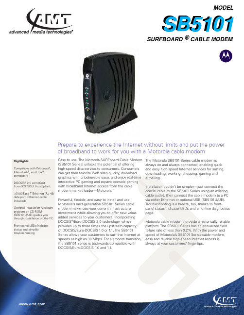
The Motorola SURFboard Cable Modem Powerful, flexible, and easy to install and use,of DOCSIS/Euro-DOCSIS 1.0 or 1.1, the SB5101 Series allows your customers to surf the Internet at speeds as high as 30 Mbps. For a smooth transition, the SB5101 Series is backwards-compatible with DOCSIS/Euro-DOCSIS 1.0 and 1.1.The Motorola SB5101 Series cable modem is e-mailing.Installation couldn’t be simpler—just connect the via either Ethernet or optional USB (SB5101U/UE)page.Motorola cable modems provide a historically reliable platform. The SB5101 Series has an annualized field speed of Motorola’s SB5101 Series cable modem, easy and reliable high-speed Internet access is always at your customers’ fingertips..Prepare to experience the Internet without limits and put the powerof broadband to work for you with a Motorola cable modemHighlightsCompatible with Windows ®, Macintosh ®, and Unix ® computersDOCSIS ® 2.0 compliant, Euro-DOCSIS 2.0 compliant 10/100Base-T Ethernet (RJ-45) data port (Ethernet cable included)Optional Installation Assistant program on CD-ROM (SB5101U/UE) guides you through installation on the PC Front-panel LEDs indicate status and simplify troubleshootingMODELSB5101SURFBOARD CABLE MODEM® Data SheetSB5101Series SURFboard Cable ModemSB5101N SeriesSB5101U Series..customer base.impact on the environmentcompliance.*Packaging. As an even shipped with each unit.* The packaging is 100% opportunities.Data SheetSB5101Series SURFboard Cable ModemGENERAL Cable Interface F-Connector, female, 75 ΩCPE Network Interface 10/100Base-T Ethernet, USB (optional)Data Protocol TCP/IP Dimensions 6.2 in H x 2.3 in W x 6.0 in D (15.75 cm x 5.84 cm x 15.24 cm)Power 9 W (nominal)INPUT POWER North America 105 to 125 VAC, 60 HzOutside North America100 to 240 VAC, 50 to 60 HzENVIRONMENTAL Operating Temperature 32 °F to 104 °F (0 °C to 40 °C)Storage Temperature –22 °F to 158 °F (–30 °C to 70 °C)Operating Humidity 5 to 95% R.H. (non-condensing)Operating Altitude –200 feet to 10,000 feet AMSL Operating Humidity 5% to 95%Power supply meets H.R.6, ENERGY STAR, and CoC (European Code of Conduct) requirements 100% recyclable packagingUnit meets CoC requirements for Energy Consumption of Broadband EquipmentUnit is RoHS compliant (lead free)DOWNSTREAM Modulation 64 or 256 QAM Maximum Data Rate** DOCSIS ≤ 38 Mbps Euro-DOCSIS ≤ 51 Mbps Bandwidth DOCSIS 6 MHz Euro-DOCSIS 8 MHz Symbol Rate DOCSIS 64 QAM 5.057 Msym/s, 256 QAM 5.361 Msym/s Euro-DOCSIS 64 QAM 6.952 Msym/s, 256 QAM 6.952 Msym/s Operating Level Range –15 to +15 dBmV Input Impedance 75 Ω (nominal)SpecificationsMOTOROLA and the Stylized M Logo are registered and Broadscape is trademarked in the US Patent & Trademark Office. SURFboard is a registered trademark of General Instrument Corporation, a wholly-owned subsidiary of Motorola, Inc. Windows is a registered trademark and Vista is a trademark of Microsoft Corporation in the U.S. and/or other countries. Linux® is a registered trademark of Linus Torvalds in the U.S. and other countries. UNIX is a registered trademark of the Open Group in the United States and other countries. Macintosh is a registered trademark of Apple Computer, Inc. DOCSIS is a registered trademark of Cable Television Laboratories, Inc. All other product or service names are the property of their respective owners. © Motorola, Inc. 2009. All rights reserved.567898-001-c 0309 5976 - 0KHighlights, continued User-friendly online diagnostics pageSupports standard Internet softwareSupports up to 63 computers on a single Internet connection (additional networking hardware required)Remote configuration and monitoring from the headend using SNMP and TFTP Stylish and space-saving enclosureMulti-language User Guide via World Wide Web, CD-ROM (optional)Optional 1.1 USB data port available (includes CD-ROM [SB5101U/UE])UPSTREAM Modulation 8****, 16, 32****, 64****, 128***** QAM or QPSK Maximum Channel Rate*** 30 Mbps Bandwidth 200 kHz, 400 kHz, 800 kHz, 1.6 MHz, 3.2 MHz, 6.4**** MHz Symbol Rates 160, 320, 640, 1280 and 2560 and 5120**** ksym/s Operating Level Range A-TDMA +8 to +54 dBmV (32 QAM, 64 QAM) +8 to +55 dBmV (8 QAM, 16 QAM) +8 to +58 dBmV (QPSK) S-CDMA +8 to +53 dBmV (all modulations)Output Impedance 75 Ω (nominal)Frequency Range DOCSIS 5 to 42 MHz (edge to edge); Euro-DOCSIS 5 to 65 MHz (edge to edge)COMPATIBILITYPC 90496, Pentium, or later; Windows Vista™, 2000,or XP; Linux ®with Ethernet connection (older versions of Windows, although not specifically supported, will work with this cable modem)Macintosh ® Power PC or later; OS 9 or higher; Ethernet connection UNIX ® Ethernet connection* Green product features are applicable to new SB5101 models, not the legacy platform.** Actual speeds will vary, and are often less than the maximum possible.Data transmission speed is approximate and depends on the configuration and capacity of your network, as well as the amount of traffic on the network.*** Actual data throughput will be less due to physical layer overhead (error correction coding, burst preamble, and guard interval).**** With A-TDMA- or S-CDMA-enabled CMTS.***** With S-CDMA-enabled CMTS.Certain features may not be activated by your service provider, and/or their network settings may limit the feature’s functionality. Additionally, certain features may require a subscription. Contact your service provider for details.All features, functionality, and other product specifications are subject to change without notice or obligation.COMPLIANTAdvanced Media Technologies, Inc.。
电源管理芯片型号
电源管理芯片型号电源管理芯片是一种用于控制和管理电源供应的集成电路,常用于电子设备和计算机系统中。
它能够监测电源电压、电流和温度等参数,以确保电子设备或计算机系统正常工作,并保护设备免受过电压、过电流和过温等不良条件的损害。
电源管理芯片的型号有很多种,下面简单介绍几种常见的型号。
1. MAX77650:这是一款高性能、集成度很高的电源管理芯片。
它具有多种功能,包括锂电池充放电管理、电源管理和系统监测等。
它采用低功耗设计,能够延长电池寿命,同时提供多种省电模式。
2. TPS54160:这是一款高效率、同步降压型电源管理芯片。
它适用于工业和通讯设备,能够提供稳定的电源输出。
它的主要特点是高效率和低纹波,能够满足电子设备对稳定电源的要求。
3. LT3652:这是一款微型化、高效率的电源管理芯片。
它适用于锂电池充电和电源管理。
它采用了开关电源技术,能够提供高效率的电源转换,同时集成了多种保护机制,能够确保电子设备的安全使用。
4. LTC6804:这是一款用于电池管理的芯片。
它可以对电池进行均衡充放电,并能够监测电池的电压、温度和容量等参数。
它采用高精度的ADC技术,能够提供准确的电池状态监测。
5. BQ25895:这是一款专用于充电管理的芯片。
它支持快速充电和逆变充电模式,能够根据不同设备的需求,选择合适的充电模式。
同时,它还具有多种保护机制,能够保护设备免受过充、过放和短路等不良条件的损害。
以上仅是部分电源管理芯片的型号介绍,每一款型号都有自己的特点和应用场合。
随着电子设备的不断发展,电源管理芯片的功能和性能也在不断提高,以满足电子设备对高效、稳定和安全电源供应的需求。
最新-MSK5101系列大电流低压差稳压器及其应用 精品
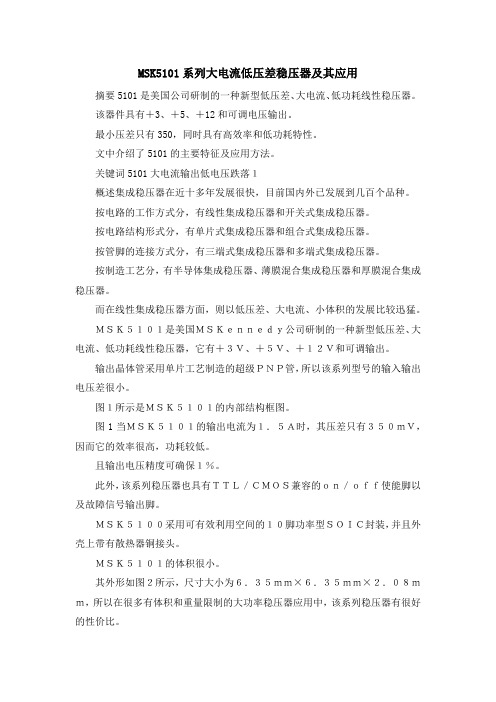
MSK5101系列大电流低压差稳压器及其应用摘要5101是美国公司研制的一种新型低压差、大电流、低功耗线性稳压器。
该器件具有+3、+5、+12和可调电压输出。
最小压差只有350,同时具有高效率和低功耗特性。
文中介绍了5101的主要特征及应用方法。
关键词5101大电流输出低电压跌落1概述集成稳压器在近十多年发展很快,目前国内外已发展到几百个品种。
按电路的工作方式分,有线性集成稳压器和开关式集成稳压器。
按电路结构形式分,有单片式集成稳压器和组合式集成稳压器。
按管脚的连接方式分,有三端式集成稳压器和多端式集成稳压器。
按制造工艺分,有半导体集成稳压器、薄膜混合集成稳压器和厚膜混合集成稳压器。
而在线性集成稳压器方面,则以低压差、大电流、小体积的发展比较迅猛。
MSK5101是美国MSKennedy公司研制的一种新型低压差、大电流、低功耗线性稳压器,它有+3V、+5V、+12V和可调输出。
输出晶体管采用单片工艺制造的超级PNP管,所以该系列型号的输入输出电压差很小。
图1所示是MSK5101的内部结构框图。
图1当MSK5101的输出电流为1.5A时,其压差只有350mV,因而它的效率很高,功耗较低。
且输出电压精度可确保1%。
此外,该系列稳压器也具有TTL/CMOS兼容的on/off使能脚以及故障信号输出脚。
MSK5100采用可有效利用空间的10脚功率型SOIC封装,并且外壳上带有散热器铜接头。
MSK5101的体积很小。
其外形如图2所示,尺寸大小为6.35mm×6.35mm×2.08mm,所以在很多有体积和重量限制的大功率稳压器应用中,该系列稳压器有很好的性价比。
液晶电源的电源管理芯片集
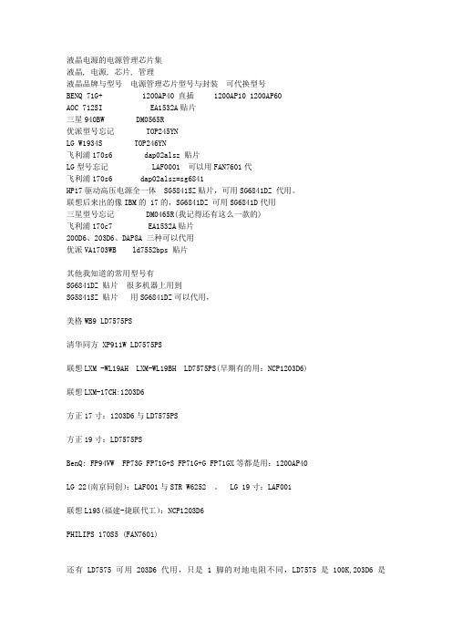
液晶电源的电源管理芯片集液晶, 电源, 芯片, 管理液晶品牌与型号电源管理芯片型号与封装可代换型号BENQ 71G+ 1200AP40 直插 1200AP10 1200AP60AOC 712SI EA1532A贴片三星940BW DM0565R优派型号忘记 TOP245YNLG W1934S TOP246YN飞利浦170s6 dap02alsz 贴片LG型号忘记 LAF0001 可以用FAN7601代飞利浦170s6 dap02alsz=sg6841HP17驱动高压电源全一体 SG5841SZ贴片,可用SG6841DZ 代用。
联想后来出的像IBM的 17的,SG6841DZ 可用SG6841D代用三星型号忘记 DM0465R(我记得还有这么一款的)飞利浦170c7 EA1532A贴片200D6、203D6、DAP8A 三种可以代用优派VA1703WB ld7552bps 贴片其他我知道的常用型号有SG6841DZ 贴片很多机器上用到SG5841SZ 贴片用SG6841DZ可以代用,美格WB9 LD7575PS清华同方 XP911W LD7575PS联想LXM -WL19AH LXM-WL19BH LD7575PS(早期有的用:NCP1203D6)联想LXM-17CH:1203D6方正17寸:1203D6与LD7575PS方正19寸:LD7575PSBenQ: FP94VW FP73G FP71G+S FP71G+G FP71GX等都是用:1200AP40LG 22(南京同创):LAF001与STR W6252 。
LG 19寸:LAF001联想L193(福建-捷联代工):NCP1203D6PHILIPS 170S5 (FAN7601)还有LD7575可用203D6代用,只是1脚的对地电阻不同,LD7575是100K,203D6是24.1K,LP7552可用SG6841代用希望大家都列下来,这样子备PWM IC的时候就有个数了,知道买什么样子的电源管理芯片备用着,有时候手上没有,知道是电源管理坏了在那里干着急,。
英飞凌推出搭载PFC功能的高压谐振控制器,适用于LED驱动器
英飞凌推出搭载PFC功能的高压谐振控制器,适用于LED驱动器英飞凌科技股份有限公司(FSE:IFX / OTCQX:IFNNY) 通过引入ICL5101,拓展了其在40W 到 300W 照明系统的控制IC产品组合。
该款新型高压谐振控制IC ICL5101高度集成化,有助于降低系统成本。
其典型应用包括:室内及室外LED 照明、高/低棚照明、街道照明、停车场及天棚照明、办公室照明、零售以及商店照明。
照明系统的总体拥有成本是工业照明的重要考量因素,而新型ICL5101 所支持的谐振拓扑效率高达95%,因此备受客户青睐。
高度集成的ICL5101可实现LED 驱动器的高端设计,相比于同时需要独立PFC IC和谐振IC 的类似解决方案,其所需元件减少约25%。
这使得设计更加可靠,从而减小了形状尺寸,简化PCB布局并降低成本。
ICL5101 集成了半桥及PFC 门极驱动器。
该IC的所有运行参数可由简单电阻进行调节,从而降低成本并保证参数设置的可靠性与稳定性。
芯片结温范围为-40°C 至+125°C,适于户外使用。
LED控制器ICL5101 专用于控制谐振拓扑例如LLC。
集成式数字化PFC单元在临界导通模式(CrCM) 和断续导通模式(DCM) 中均可运行,因此在装置变暗等情况导致的低负载状态下仍可进行极为稳定的调节。
LED照明亮度可在其额定负载100%至0.1%的大范围内进行调节。
市场上现有最新调光技术范围一般只实100%到5%。
此外,ICL5101还可在任何条件下以极短时间(小于200 ms)点灯。
ICL5101可调式PFC单元可输出优质电能,在宽输入电压范围内实THD低于10%功率因素超过0.99 ,从而助力照明设备生产商达到能效标准。
此外,ICL5101 在输入电压变化时保证输出极为稳定。
外部过温保护和容性负载保护等一系列保护功能确保及时检测出故障状态、提升系统安全。
此次英飞凌推出ICL5101,再次展现了其在高效LED驱动器解决方案领域的技术领军地位。
TRM-5101AG中文资料
Optoway TRM-5101G**********************************************************************************************************************************************************************************************************************************************************************************************************************************************OPTOWAY TECHNOLOGY INC. No .38, Kuang Fu S. Road, Hu Kou, Hsin Chu Industrial Park, Hsin Chu, Taiwan 303Tel: 886-3-5979798 Fax: 886-3-59797371TRM-5101G / TRM-5101TG / TRM-5101AG / TRM-5101ATG3.3V / 1310 nm / 622 Mbps RoHS Compliant Optical Multi-Mode Transceiver***********************************************************************************************************************************************************************FEATURESl Duplex SC Multimode Transceiver : TRM-5101G l Duplex ST Multimode Transceiver :TRM-5101TG l 1310 nm Transmitter l 0 to 1000 m Transmissionl Industry Standard 1 x 9 Footprint l Single +3.3 V Power Supply l PECL Signal Detection Output l RoHS Compliantl 0 to 70o C Operating : TRM-5101G l -40 to 85o C Operating : TRM-5101AG l Wave Solderable and Aqueous Washablel Class 1 Laser International Safety Standard IEC 60825 CompliantAPPLICATIONSl ATM 622 Mbps Linksl SONET/SDH Equipment Interconnect l Fast Ethernet 100 Mb/s LinksDESCRIPTIONThe TRM-5101G series multi-mode transceivers are low power, high performance module for bi-directional serial optical data communications such as ATM 622 Mb/s, Fast Ethernet and Fibre Channel. This module is designed for multi-mode fiber and operates at a nominal wavelength of 1310 nm. The transmitter section uses a multiple quantum well laser and is a class 1 laser compliant according to International Safety Standard IEC 60825. The receiver section uses an integrated InGaAs detector preamplifier (IDP) mounted in an optical header and a limiting post-amplifier IC. A PECL logic interface simplifies interface to external circuitry.LASER SAFETYThis multi-mode transceiver is a Class 1 laser product. It complies with IEC 60825 and FDA 21 CFR 1040.10 and 1040.11. The transceiver must be operated within the specified temperature and voltage limits. The optical ports of the module shall be terminated with an optical connector or with a dust plug.ORDER INFORMATIONP/No.Bit Rate (Mb/s) Distance (m) Wavelength (nm) Voltage (V) ConnectorTemp. (o C)TX Power (dBm)RX Sens. (dBm) RoHS Compliant TRM-5101G 622 0 to 1000 1310 3.3 1X9 SC/ST 0 to 70 -12 to -19 -26 Y TRM-5101AG6220 to 100013103.31X9 SC/ST -40 to 85 -12 to -19 -26YAbsolute Maximum RatingsParameterSymbol Min Max Units NotesStorage Temperature Tstg -40 85 o COperating Temperature Topr 0 -40 70 85 o CTRM-5101G TRM-5101AGSoldering Temperature --- 250 oC 10 seconds on leads only Power Supply Voltage Vcc 0 4.5 V Input Voltage --- GND Vcc VOutput CurrentIout30mARecommended Operating ConditionsParameterSymbol Min Typ Max Units Power Supply Voltage Vcc 3.13 3.3 3.47 VOperating Temperature Topr0 -40 70 85 oC / TRM-5101G oC / TRM-5101AGData Rate100622Mb/sTransmitter Specifications (0o C < Topr < 70o C, 3.13V < Vcc < 3.47V)Parameter Symbol Min Typ Max Units NotesOpticalOptical Transmit Power Po -19 --- -12 dBm 1Output Center Wavelength λ1260 1310 1360 nmOutput Spectrum Width ∆λ--- --- 10 nm RMS (σ)Extinction Ratio E R8.2 --- --- dBOutput Eye Compliant with Bellcore TR-NWT-000253 and ITU recommendation G.957Optical Rise Time t r 1.2 ns 10% to 90% Values Optical Fall Time t f 1.2 ns 10% to 90% Values Relative Intensity Noise RIN -116 dB/HzTotal Jitter TJ 0.55 ns 2ElectricalPower Supply Current Icc 140 mA 3Data Input Current – Low I IL-350 µAData Input Current – High I IH350 µADifferential Input Voltage V IH - V IL300 mVData Input Voltage – Low V IL - V CC-2.0 -1.58 V 4Data Input Voltage -- High V IH - V CC-1.1 -0.74 V 4Notes: 1. Output power is power coupled into a 62.5/125 µm multi-mode fiber.2. Measured with a 223-1 PRBS with 72 ones and 72 zeros.3. Maximum current is specified at Vcc = Maximum @ maximum temperature.4. These inputs are compatible with 10K, 10KH and 100K ECL and PECL inputs.Receiver Specifications(0o C < Topr < 70o C, 3.13 V < Vcc < 3.47V)Parameter Symbol Min Typ Max Units NotesOpticalSensitivity--- --- -28 -26 dBm 1Maximum Input Power Pin -8 --- --- dBmSignal Detect -- Asserted Pa --- --- -26 dBm Transition: low to high Signal Detect -- Deasserted Pd -40 --- --- dBm Transition: high to low Signal detect -- Hysteresis 1.0 --- 4.0 dBWavelength of Operation 1100 --- 1600 nmElectricalPower Supply Current Icc 100 mA 2Data Output Voltage – Low V OL - V CC-2.0 -1.58 V 3Data Output Voltage – High V OH - V CC-1.1 -0.74 V 3Signal Detect Output Voltage -- Low V OL - V CC-2.0 -1.58 VSignal Detect Output Voltage -- High V OH - V CC-1.1 -0.74 VNotes: 1. Minimum sensitivity and saturation levels at BER=1E-10 for a 223-1 PRBS.2. The current excludes the output load current.3. These outputs are compatible with 10K, 10KH and 100K ECL and LVPECL outputs.*********************************************************************************************************************************************************************** OPTOWAY TECHNOLOGY INC. No.38, Kuang Fu S. Road, Hu Kou, Hsin Chu Industrial Park, Hsin Chu, Taiwan 303Tel: 886-3-5979798 Fax: 886-3-5979737CONNECTION DIAGRAMReceiver Signal Ground 1 (Rx GND)Receiver Data Out 2 (RD+) N/CReceiver Data Out Bar 3 (RD−)Signal Detect 4 (SD)Receiver Power Supply 5 (Rx Vcc) TOP VIEWTransmitter Power Supply 6 (Tx Vcc)Transmitter Data In Bar 7 (TD−)Transmitter Data In 8 (TD+) N/CTransmitter Signal Ground 9 (Tx GND)*********************************************************************************************************************************************************************** OPTOWAY TECHNOLOGY INC. No.38, Kuang Fu S. Road, Hu Kou, Hsin Chu Industrial Park, Hsin Chu, Taiwan 303Tel: 886-3-5979798 Fax: 886-3-5979737*********************************************************************************************************************************************************************** OPTOWAY TECHNOLOGY INC. No.38, Kuang Fu S. Road, Hu Kou, Hsin Chu Industrial Park, Hsin Chu, Taiwan 303Tel: 886-3-5979798 Fax: 886-3-5979737TRM-5101TG / TRM-5101ATGNote: Specifications subject to change without notice.*********************************************************************************************************************************************************************** OPTOWAY TECHNOLOGY INC. No.38, Kuang Fu S. Road, Hu Kou, Hsin Chu Industrial Park, Hsin Chu, Taiwan 303Tel: 886-3-5979798 Fax: 886-3-5979737。
XC5101-1A线性锂离子电池充电器
XC5101_______________________________________________________XC5101- 1A Linear Li-Ion Battery Charger GENERAL DESCRIPTIONThe XC5101 is a complete constant current &constant voltage linear charger for single cell lithium-ion batteries. Its SOP package and low external component count make the XC5101 ideally suited for portable applications.Furthermore, the XC5101 is specifically designed to work within USB power specifications.No external sense resistor is needed, and no blocking diode is required due to the internal MOSFET architecture. Thermal feedback regulates the charge current to limit the dietemperature during high power operation or high ambient temperature. The charge voltage is fixed at 4.21V, and the charge current can beprogrammed externally with a single resistor. The XC5101 automatically terminates the charge cycle when the charge current drops to 1/10th the programmed value after the final float voltage is reached.When the input supply (wall adapter or USB supply) is removed, the XC5101 automatically enters a low current state, dropping the battery drain current to less than 2uA. The XC5101 can be put into shutdown mode, reducing the supply current to 50uA.Other features include Battery temperature monitor, under-voltage lockout, automaticrecharge and two status pins to indicate charge and charge termination.FEATURESProgrammable Charge Current Up to 1000mANo MOSFET, Sense Resistor or Blocking DiodeComplete Linear Charger in SOP Package for single Cell Lithium-Constant-Current/Constant-Voltage Operation with Thermal Regulation to Maximize ChargeRate Without Risk of OverheatingCharges Single Cell Li-Ion Batteries Directly fromPreset 4.21V Charge Voltage with ±1% AccuracyCharge Current Monitor Output for Gas GaugingCharge state pairs of output, no battery and faultC/10Soft-Available in SOP8-PP PackageAPPLICATIONSCellular Telephones, PDAs, MP3 /MP4 PlayersCharging Docks and Cradles Bluetooth 、GPS ApplicationsFigure1Typical Application Circuit深圳市思微半导体有限公司XC5101 ______________________________________________________________________________________________________________________ ORDERING INFORMATIONPART NUMBER TEMP RANGE VIN VBATCHARGECURRENTPACKAGE PINSXC5101 -40°C to 85°C 4.5~6V 4.21V 1A SOP-PP 8 PIN CONFIGURATIONFigure 2. PIN ConfigurationPIN DESCRIPTIONPIN NUMBERPINNAMEPIN DESCRIPTION1, TEMP Battery temperature detection input2 PROG Charge Current Program, Charge Current Monitor and Shutdown Pin.3 GND Ground4 VCC Positive Input Supply Voltage.5 BAT Charge Current Output.6 /STBY The completion of battery charging instructions side.7 /CHRG Open-Drain Charge Status Output.8 CE Chip enable input.9 EPAD Ground and EPADABSOLUTE MAXIMUM RATINGS(Note: Do not exceed these limits to prevent damage to the device. Exposure to absolute maximum rating conditions for long periods may affect device reliability.)PARAMETER VALUE UNIT Input Supply Voltage VCC VSS-0.3~VSS+7 V PROG pin Voltage Vprog VSS-0.3~Vcc+0.3 V BAT pin Voltage Vbat Vss-0.3~7 VCHAG pin Voltage Vchrg VSS-0.3~VSS+7 V BAT pin Current Ibat 1.4 A PROG pin Current Iprog 1.4 mA Operating Ambient Temperature -40 to 85 °C Maximum Junction Temperature 150 °C Storage Temperature -55 to 150 °C Lead Temperature (Soldering, 10 sec) 260 °CELECTRICAL CHARACTERISTICS(V IN = 3.6V, T A= 25 C unless otherwise specified)PARAMETER SYMBOL TEST CONDITIONS MIN TYP MAX UNIT Input Voltage Range VCC 4.25 6.5 VInput supply current Icc Charge mode, RPROG =10K 350 2000 uA Standby mode 150 500 uA Shutdown mode(RPROG notconnected,Vcc<Vbat or Vcc<Vuv)50 100 uABAT pin Current Ibat R PROG =2k,Current mode 450 500 550 mA R PROG =1k,Current mode 900 1000 1100 mA Standby mode,Vbat=4.2V 0 -2.5 -6 uA Shutdown mode 1 2.5 uA Sleep mode,Vcc=0V 0.3 2.5 uARegulated Charge Voltage Vfloat 0°C≤TA≤85°C, Icharge = 40mA 4.178 4.21 4.242 V PROG pin Voltage Vprog R PROG =1k, Current mode 0.93 1.0 1.07 VTrickle charge current Itrikl Vbat<Vtrikl,Rprog=1k 90 100 110 mA Trickle charge ThresholdVoltageVtrikl R PROG =10K,Vbat Rising 2.8 2.9 3.0 V Trickle voltage hysteresisvoltageVtrhys R PROG =10K 60 80 110 mV Recharge Battery thresholdVoltageΔVrecg V FLOAT - V RECHRG150 300 mV CHRG pin Output lowvoltageVchrg Ichrg=5mA 0.35 0.6 V STDBY pin Output lowvoltageVstdby Istdby=5mA 0.35 0.6 V Enable Threshold VCC=4.25V~6.5V 0.3 1 1.5 V Enable Leakage Current -0.1 +0.1 uATEMP pin voltage of the high-end flip Vtemp-h 80 82 %VccPIN FUNCTIONTEMP (PIN 1): Battery temperature detection input.TEMP pin to receive the battery NTC sensor output.If the TEMP pin voltage is less than the input voltage is greater than 45% or 80% of the input voltage means the battery temperature is too low or too high, then the charge has been suspended.If the TEMPdirect access GND, battery temperature detection canceled, the other charged and functioning properly.PROG (PIN 2): Charge Current Program, Charge Current Monitor and Shutdown Pin.The charge current is programmed by connecting a 1% resistor, RPROG, to ground. When charging in constant-current mode, this pin servos to 1V. In all modes, the voltage on this pin can be used to measure the charge current using the following formula: IBAT = (VPROG/RPROG) x1000.The PROG pin can also be used to shut down the charger. Disconnecting the program resistor from ground allows a 3uA current to pull the PROG pin high. When it reaches the 1.21V shutdown threshold voltage, the charger enters shutdown mode, charging stops and the input supply current drops to 50uA. This pin is also clamped to approximately 2.4V. Driving this pin to voltages beyond the clamp voltage will draw currents as high as 1.5mA. Reconnecting RPROG to ground will return the charger to normal operation.GND (PIN 3): Ground.VCC (PIN 4): Positive Input Supply Voltage.Provides power to the charger, VCC can range from 4.25V to 6.5V and should be bypassed with at least a 10uF capacitor. When VCC drops to within 30mV of the BAT pin voltage, the XC5101 enters shutdown mode, dropping IBAT to less than 2uA.BAT (PIN 5): Charge Current Output.Provides charge current to the battery and regulates the final float voltage to 4.2V. An internal precision resistor divider from this pin sets the float voltage which is disconnected in shutdown mode.STDBY (PIN 6): The completion of battery charging instructions side.When the battery charge is complete, STDBY pulled low by internal switches, indicating the completion of charging. In addition, STDBY pin will be in a high-impedance state.CHRG (PIN 7): Open-Drain Charge Status Output.When the battery is charging, the CHRG pin is pulled low by an internal N-channel MOSFET. When the charge cycle is completed, CHRG pin will be in a high-impedance state.CE (PIN 8): Chip enable input.High input level will make XC5101 in normal working condition; low input level so that XC5101 is prohibited charging status. CE pin can be TTL or CMOS level-level driver.TEMP pin voltage of the low-end flipVtemp-l4345%Vc cTYPICAL PERFORMANCE CHARACTERISTICSBATTERY CHARGER CURVEPACKAGE OUTLINESOP8-PP PACKAGE OUTLINE AND DIMENSIONSIn order to increase the driver current capability of XC5101 and improve thetemperature of package, Please ensure Epad and enough ground PCB to release energy.SYMBOLDimension inMillimeters Dimension inInches MIN MAXMIN MAX A 1.300 1.700 0.051 0.067 A1 0.000 0.100 0.0 0.004 A2 1.350 1.550 0.053 0.061 B 0.330 0.510 0.013 0.020 C 0.170 0.250 0.007 0.010 D 4.700 5.100 0.185 0.201 E 3.800 4.000 0.150 0.157 E1 5.800 6.200 0.228 0.244 e 1.27 TYP 0.050 TYP L 0.400 1.270 0.016 0.050 0o 8o 0o 8o F 2.313 2.513 0.091 0.099 G 3.202 3.4020.126 0.134XC5101 ______________________________________________________________________________________________________________________ PROUCT CHANGE NOTICE LISTNO Updated date Version update Update content1 2013-10-24 Rev 0.1 Create datasheet2 2013-12-16 Rev 0.2 Update Vbat Parameter value。
L5101中文资料
UNISONIC TECHNOLOGIES CO., LTDL5101 LINEAR INTEGRATED CIRCUITWHITE LED STEP-UP CONVERTERDESCRIPTIONThe UTC L5101 is a fixed frequency step-up PWM DC/DC converter and designed for white LEDS driving with a constant current to provide backlight in handheld devices. The device switches at a high frequency 1.2MHz by an internal N-channel MOSFET switch to be capable of minimum external components using.The UTC L5101 can drive up to 5 LEDs in series by a Li-Ion cell. Series connection of LEDS provides identical LED currents resulting in uniform brightness without ballast resistors. The low 95mV feedback voltage minimizes power loss in the current setting resistor can have better efficiency.FEATURES* Built-In Open Circuit Protection * Built-In Over Voltage Protection* High Efficiency(Up to 84% at V IN =4.2V, 3 LEDs, I LED =20mA) * 1.2MHz fixed switching frequency * Low supply current: 70µA * Matches LED current* Requires tiny inductor and capacitors*Pb-free plating product number: L5101LORDERING INFORMATIONOrder NumberNormal Lead Free PlatingPackage PackingL5101-AG6-R L5101L-AG6-R SOT-26 Tape ReelPIN CONFIGURATIONOVP SHDNGNDFBVPIN DESCRIPTIONSBLOCK DIAGRAMV INFBOVPTEST CIRCUITL1V INC20.22 FD1APPLICATION INFORMATIONRecommended Component SelectionInductor Selection: A 10µH inductor is recommended for most applications.Capacitor Selection: The small size of ceramic capacitors (1µF input with 1µF output ) are sufficient, X5Rand X7R types are recommended Diode Selection: An Schottky diode rated at 100mA ~ 200mA is sufficient for most applications. LED Current ControlA feedback resistor (precision 1% recommended) as feedback resistor control the LED current.(R FB in Figure 1) - Feedback reference voltage : 95mV. - LED current is 95mV/R FB .- The formula for R FB selection : R FB =95mV/I LEDLV INC2 1 FFig.1 Dimming Control with a PWM SignalOpen-Circuit ProtectionWhen a high output voltage exceeds maximum 33V, the built-in OVP (Over Voltage Protection) will be triggered to prevent the damage resulting from an open circuit condition. Dimming ControlThere are three different ways of dimming control circuits as follows: 1. Using a PWM signalV INL Fig.2 Dimming Control Using a PWM SignalAPPLICATION INFORMATION(Cont.)2. Using a DC VoltageV INC2 1 FLFig.3 Dimming Control Using a DC Voltage3. Using a Filtered PWM SignalV INC2 1 FLFig.4 Dimming Control Using a Filter PWM SignalTYPICAL CHARACTERISTICS3060Supply Voltage (V)507040S u p p l y C u r r e n t (μA )Supply Current vs. Supply Voltage (V)0.61.4Supply Voltage (V)1.01.60.8S up p l y C u r r e n t (m A )Supply Current vs . Supply Voltage (V)1.20.82.54.05.03.51.3Supply Voltage (V)1.11.4 6.00.9R D S O N (O )R DS-ONvs. Supply Voltage (V)4.55.53.01.01.26015585LED Current (mA)75902065E f f c i e n c y (%)3 LEDs Efficiency vs. LED Current1070806085LED Current (mA)759065E f f c i e n c y (%)3 LEDs Efficiency vs. LED Current70806085LED Current (mA)759065E f f c i e n c y (%)4 LEDs Efficiency vs. LED Current7080TYPICAL CHARACTERISTICS(cont.)6015585LED Current (mA)75902065E f f c i e n c y (%)5 LEDs Efficiency vs. LED Current107080。
基准电源常用芯片
基准电源常用芯片
基准电源芯片(也称作电压基准源或参考电压源)是电子电路中用于提供精确、稳定且温度系数极低的固定输出电压的集成电路。
这类芯片在许多需要高精度和长期稳定的系统中扮演着重要角色,例如仪表仪器、数据转换器(ADC/DAC)、电源管理以及各类精密模拟电路。
以下是一些常见的基准电压芯片:
1. LM236系列:
LM236D-2.5, LM236DR-2.5, LM236LP-2.5:这些是Texas Instruments(TI)生产的2.5V基准电压源芯片,具有较宽的工作电流范围(400uA~10mA)。
2. LM285系列:
LM285D-1.2, LM285D-2.5, LM285LP-2.5:这些是微功耗电压基准芯片,适用于电流需求较低的应用,工作电流范围为10uA至20mA。
3. LM336系列:
LM336BD-2.5:同样是TI的一款2.5V基准电压源,具有与LM285类似的微功耗特性,工作电流也在10uA至20mA之间。
4. 其他典型基准电压芯片:
MC1403:摩托罗拉(现NXP)生产的2.5V基准电压源。
TL431:一个精密可调基准稳压源,其输出电压可在2.5V至36V范围内调节,广泛应用于各种电源控制和保护电路中。
AZ431BN-ATRE1:可能是ADI公司的一款高精度电压基准芯片。
- 1、下载文档前请自行甄别文档内容的完整性,平台不提供额外的编辑、内容补充、找答案等附加服务。
- 2、"仅部分预览"的文档,不可在线预览部分如存在完整性等问题,可反馈申请退款(可完整预览的文档不适用该条件!)。
- 3、如文档侵犯您的权益,请联系客服反馈,我们会尽快为您处理(人工客服工作时间:9:00-18:30)。
一、功能概述 低启动电流和工作电流 内置前沿消隐(LEB)
内置峰值电流补偿和同步斜坡补偿 内置抖频功能可以降低EMI 逐周期限制电流
空载或轻载时降频和跳周期工作模式 异常过流保护
过压、欠压、开环、过载、过温、输出短路等保护;
二、特性描述
TM5101是一款高集成度、高性能的PWM 的电流型开关电源控制器。
适用于充电器、电源适配器等各类小功率的开关电源。
采用DIP8和SO-8封装,完善的保护功能,电路结构简单,成本低。
待机功率低,符合“能源之星”等待机功耗标准要求。
三、典型应用
四、产品封装形式及引脚功能
采用SOP-8和DIP-8封装
管脚序号
名称
功能描述
1 FB 电压反馈引脚,通过连接光耦到地来调整占控比。
2、6、7
NC
空脚。
3 VDD
电源供电输入脚 4 GATE
驱动输出脚,外接MOSFET 5 CS 电流检测引脚(MOS 源极),外接电阻来检测MOS 电流 8 GND 接地引脚
GND CS
NC NC VDD FB NC
五、内部框图
六、极限参数及推荐值
注意:极限参数是定义芯片的工作的极限值,超过这些工作条件时将会使电路功能失常,甚至造
成损坏,因此,实际的应用中必须低于推荐值。
符号参数推荐值极限值单位
V DD供电电压10~23 30 V
V FB FB引脚输入电压0~5.5 -0.3~ 7.0 V
V CS CS引脚输入电压-0.3 ~ 5.0 V
θJC热阻(结点到外壳) 82.5 °C/W
T J工作结点温度-40 ~ +150 °C
T STG 存储温度范围-40~ +150 °C
°C
+130
-40~
T A工作环境温度 -20~+80
T L焊接温度(10秒) 260 °C
人体模式, JESD22-A114 2.0
ESD 抗静电能力
kV
机器模式, JESD22-A115 0.2
七、电气参数
(如非特别指明均指V DD =15V ,T A =25℃)
符号 参数
测试条件
最小值 典型值 最大值
单位
供电部份 V DD-ON 启动电压 13.5 14.5 15.5 V
V DD-OFF 关闭电压 8 9 10 V I DD-ST 启动电流 V DD =V DD-ON – 0.5V
5
20
uA
I DD-OP 正常工作电流 2.5 4 mA
V DD-OVP
V DD 过压保护
23 24 V
V DD-CLAMP V DD 钳位电压 I DD =5mA 25 27 V
V DD-BM V DD 跳周期模式电压
10 V 反馈部份 A V
PWM 比较器增益
1.7 V/V Z FB FB 引脚输入阻抗
6.0
k Ω
V FB-OPEN FB 开路电压 4.4 4.7 5.0 V V FB-PL FB 过载电压阀值 3.7 V T PD 过载延时时间
50 ms V FB-BM
进入跳周期模式FB 电压
1.4
V
电流检测部份
Z CS CS 引脚输入阻抗
5.0 k Ω V CSTH-H 电流限流值(最大占空比)
1.0
1.1
V V CSTH-L 电流限制值(最小占空比) 0.7 0.8 V T LEB 前沿尖峰消隐时间
350
ns
T PD 延时输出时间
60 ns
八、功能描述
启动电压及电流
典型的启动电流为5uA ,可以使用阻值较大而功耗较小的启动电阻,以减小功率损耗。
当
V DD 电压上升到15.5V 时,电路开始启动工作,V DD 滤波电容持续对电路供电直到由变压器的辅助绕组提供电流。
在此期间V DD 电压不能低于9.5V 。
一个1.5~2M Ω,0.25W 的启动电阻和一个10uF/25V 的电解电容可满足电源的启动需要。
振荡部份 f OSC 振荡频率 62 67 72 kHz f OSC-BM 跳周期振荡频率 20 kHz f △shuffling 抖频范围
6 % f DV 频偏 vs V DD 电压
V DD =10V to 23V
0.2
1
%
输出部份 D MAX 最大占空比
75 80 85 %
V OL 输出低电压 V DD =15V ,I O =20mA 1.5 V V OH 输出高电压 V DD =15V ,I O =20mA 10
V
t R V DD =15V ,C L =1nF 240 uS t F
V DD =15V ,C L =1nF 75 uS V G-CLAMP 输出钳位电压
17 18 V
轻载跳周期工作
在空载或轻载的情况下,FB的电压自动降低。
当V FB < 1.4V且V DD> 10 V时电路会进入间歇振荡状态,震荡输出将停止一段时间,减少开关次数,降低开关损耗。
当V FB>1.4V时,电路进入正常工作状态。
振荡频率和抖频
内置工作频率典型值为67KHz,由于频率抖动功能的作用,开关频率在63K到71K之间变化,以减小某一个频率点对外的辐射,从而降低了EMI,更容易满足设计要求,
前沿消隐
在MOS开启的瞬间,由于寄生电容和次级整流管反向恢复时间等原因,在电流检测电阻上将会有一个尖峰电压。
TM5101内置了350nS的前沿消隐电路,可以屏蔽尖峰电压,避免了电路的误动作,省去了常用的RC滤波器。
峰值电流补偿
由于电路内部的信号传送延时,使电感电流发生额外过冲。
传播延时的时间并不因输入电压变化而变化,但电感电流的过冲量随输入电压升高而陡增,高输入电压和低输入电压条件下的最大输出功率相差甚远。
TM5101通过引入一个动态变化的斜坡电压来均衡高低压输出特性。
过流检测电压限值随占空比的变化从0.8~1.0V
斜坡补偿
在CCM状态下工作时,如果占空比大于50%时,电路容易出现次谐波振荡,TM5101内置斜坡补偿电路可以有效防止次谐波振荡的出现。
V DD过压、欠压保护
当V DD>23V时,电路会进入过压保护,输出脉冲会立即停止,直到V DD掉到欠压后电路重新启动,另外V DD还设置了钳位电路,防止过高的V DD冲击电压损坏电路。
如果V DD电压下落到8.5V以下时电路将会发生欠压保护,电路停止工作。
逐周期电流限制保护
在每个周期,峰值电流都不会超过峰值电流限流值。
当电流达到峰值限流电流后,输出功率就不能再变大,导至FB的电压升高,发生过载保护。
过载或系统开环保护、输出短路保护
当发生开环(反馈环路发生故障,如光耦开路)、过功率、输出短路等异常时,FB引脚的电压会上升,当V FB>3.7V 时,将恒定输出功率,如果此异常维持50mS以上,电路关闭输出,直到V DD欠压后电路重新启动。
九、应用实例 输入电压:90~264VAC
输出:12V1.5A 空载损耗:<0.3W 效率:>80%(满载) 原理图
1000UF/16V
C6
C3
4.7nF
+C2
10U/50V
U2
PC817 C
10
8
2
6
13T1
EF20
Y1
R11R12360R 1/8W
Q14N60
R100.9R 1% 1W
CX1
R6
10R
D51N4007
D7FR107
D8MBR10100
R720R 1/4W
D61N4148
R51k 1/8W
GND FB
1
2
TM5105
变压器结构图
骨架
骨架:EF20(5+5)
磁芯:EF20(PC40)漏感: PIN1-PIN3 80uH max (其它脚短路)
108
屏蔽 Φ0.15绕满一层电感量: PIN1-PIN3 L=800uH±10%
5
4
31
十、封装尺寸
DIP8
绿色低功耗开关电源控制器 TM5101
- 11 -
SOP-8
(以上电路及规格仅供参考,如本公司进行修正,恕不另行通知。
)。