纳米腔带波导耦合2014-04-16
纳米尺度波导
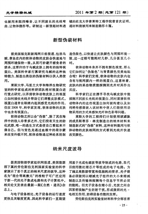
时, 金属纳米结构 的表面会产生带 电的等离 型仅 为 5 6 0× 0平 方 纳 米 , 一 个 金 属 一绝 在 半导体设备 内 , 可见光 和近红外线波 子体 , 等离子体又可与光子相互作用 , 形成被 缘体 一 称为表面等离子体激元 (P ) SP 的准粒子 , 从而 段的光可产生纳米尺度 的波导。该 H P模 P 可将光子 的波长缩小 到衍射极 限以下 , 减少 式能够减少衍射干扰而且光信号损失较少 , 衍射 干 扰 。但 光 信 号 在 通 过 金 属/ 质 表 面 其不 仅对 小型 设 备 有 优 势 , 介 而且 为纳 米 激 光 的金属 那部分 时 , 其强 度却 会减弱 。 器 的研制 铺 平 了道 路 , 时 , 可 用 于 制 造 同 还 单 为 了解 决 光子 信 号 损 失 的 问题 , 翔 团 量子 光学 设备 、 光 子 全 光 学 开关 和分 子 传 张 队提 出 了 混 合 等 离 子 激 元 ( P) 概 念 。 感器 等 。 HP 的 这种 HP P波 导 系统 完 全 可 以 同现 有 的 个 半 导体 ( 介 质 ) 被 放 置 在 一 个 金 属 高 带 表面上 , 其 中插 入 一 薄层 氧 化 物 ( 介 半 导 互 补 式 金 属 一氧 化 层 一半 导 体 在 低 质 )这种新 的金属 一氧化物 一 导体设计 ( MO ) , 半 C S 处理 技术 以及用 于 光子 集 成 的绝 缘 会将人射光波 的能量进行重新分配 , 光波 的 硅平 台兼 容 , 因此更 容易进 行低成本 、 规 大 很 多 能量 不再 集 中于 金 属 内 ( 处 光 子 的损 模的集成和制造。索格相信 , 于这 种技术 此 基 失 非 常高 ) 而被挤 入 低 介 质 氧化 物 中 , 此 的应用 模 型将 于一 两 年 内问 世 , 个 实 际 产 , 在 首 品也将 于 五年 内上 市 。 处 。 子 的损 失要 少 很多 。 光
纳米科学与技术论坛

纳米科学与技术论坛多光子晶体耦合波导的解耦合特性于天宝1,2 ,廖清华2,周海峰1,江晓清1,王明华1(1.浙江大学信息与电子工程学系,杭州 310027;2.南昌大学物理系,南昌 330047)摘 要: 将多个光子晶体耦合波导视为多模耦合系统,采用导模传输法,分析了各波导之间出现解耦合 的条件。
耦合系统的各本征导模能近于简并,近简并频率区的光功率由于解耦合被局限在输入方向。
解耦合频率区不随耦合波导数目变化而发生变化。
关键词: 光子晶体波导,解耦合,简并原位AFM 调查自组装嵌段共聚物纳米孔薄膜的可逆pH 刺激响应王赪胤, 冒银道,王德艳,胡效亚(扬州大学化学化工学院,扬州225002)摘 要: 以小水滴为模版,在潮湿的空气中,通过聚苯乙烯-嵌段-聚丙烯酸(PS–b–PAA)分子自组装制备了纳米多孔薄膜。
通过原位AFM 图像扫描调查了该纳米多孔薄膜在不同的pH 值缓冲溶液中的微结构表面形貌变化,表明该薄膜在pH 值为2.4 – 9.2 的缓冲溶液中,纳米孔直径发生可逆的变化。
使用一个“两步法”机理讨论了膜微结构刺的激响应动力学。
通过视频接触角 (OCA)观察到薄膜表面的对水的润湿性能从疏水性变化到超级亲水性。
该研究的目标是发展一种新型具有可pH 调控的纳米多孔功能材料。
关键词: 原子力显微镜;聚苯乙烯-嵌段-聚丙烯酸;膜;刺激响应;嵌段共聚物墨鱼骨有机质中金纳米颗粒的自发形成和组装贾雪平, 钱卫平(东南大学生物科学与医学工程学院 生物电子学国家重点实验室 南京 210096)摘 要: 本文采用一种简易的方法,在没有任何其他还原剂和稳定剂的情况下,于墨鱼骨有机质中自发形成并组装了金纳米颗粒。
在环境温度下(30 ℃),将墨鱼骨有机质在氯金酸溶液中浸泡30 分钟,然后于纯水中静置七天,可使金纳米颗粒还原并组装于墨鱼骨有机质中,得到一种含金免支撑无机-有机复合材料。
材料为紫红色,吸收峰波长在535 nm 左右,保留了墨鱼骨房架中的大孔结构,具有较高的表面积。
单模光纤与SOI纳米线波导耦合设计
法。仿真分析 了光栅 的周期 、槽深 、占空比 、S 层厚度 等光 栅参数对耦合效 率的影响 ,并给 出了使输入 光 i 02 栅耦合器耦合 效率达到4. 2 %;输出光栅耦合器 的耦合效率达 到7. 的一 组最佳光栅参数 。 6 2% 3
关键词 :集成 光学 ;S g 米 线波 导 ;光栅耦合器 ;耦合效率 Olp q 中图分类 号: C4 0 文献标 识码: T 1 A
i a t f ai g p rme eso o p i g e ce c . n d c h p i l t c u e Co p i g e ce c f4 . % a d mp c t aa t r n c u l f in y a d e u e t e o t o g n r n i ma sr t r . u l f in y o 2 6 n u n i
( h o f lc o i n o u e in e n eh oo y Not iesyo C ia Ta u n0 0 5 , hn ) S o l E e t nc a d C mp tr ce c dT c n lg , r Un r t f hn , i a 3 0 1 C ia c o r s S a h v i y
C ouplng de i n t e n i l 。m ode fbe nd SO I i sg be w e sng e_ ‘ i ra
na nophot oni a g de c w ve ui s
Ca i o M n,Che Gou , n xi TongX iog n a ag
e c e y e cl w h c sb sd on usngM A TL i f inc xa ty, i h i a e i AB o r m m i om b n d w ih O PTI TD i ultn D ic st pr g a ng c ie t FD sm ai g. s us he
基于绝缘体上硅脊型纳米线光波导方向耦合器的TE_TM偏振分束器

47, 051301 (2010) ©2010 中国激光杂志社doi: 10.3788/lop47.051301基于绝缘体上硅脊型纳米线光波导方向耦合器的TE/TM偏振分束器王剑威戴道锌时尧成杨柳(浙江大学现代光学仪器国家重点实验室光及电磁波研究中心,浙江 杭州 310058)摘要利用有限元方法和时域有限差分方法,优化设计了一种结构紧凑的基于绝缘体上硅脊型纳米线光波导方向耦合器的TE/TM偏振分束器。
考虑到方向耦合器的波导间隙较小时制作工艺较为困难,且模式失配会引入一些损耗,因此波导间隙取约100 nm较为合适。
通过优化脊型纳米线光波导的几何尺寸(脊高和脊宽)、耦合区波导间隙,使得偏振分束器长度最短。
数值计算结果表明经过优化的偏振分束器最短长度大约为17.3 µm,偏振分束器的消光比大于15 dB时,波导宽度制作容差为-20~10 nm,带宽约为50 nm。
关键词集成光学;偏振分束器;方向耦合器;绝缘体上硅中图分类号 O436 OCIS 130.5440 230.1360 文献标识码 ADesign of Compact TE/TM Polarization Beam Splitter Based on Silicon-on-Insulator Ridge Nanowire Directional Coupler Wang Jianwei Dai Daoxin Shi Yaocheng Yang Liu(Centre of Optical and Electromagnetic Research, State Key Laboratory for Modern Optical Instrumentation, ZhejiangUniversity, Hangzhou, Zhejiang 310058, China)Abstract A compact TE/TM polarization beam splitter (PBS) based on a silicon-on-insulator (SOI) ridge nanowire directional coupler is designed and optimized by using a finite-element method (FEM) and a finite difference time domain (FDTD) method. Considering the fabrication precision and the mode mismatching loss in a directional coupler, a gap width about 100 nm is chosen. The ridge height, the ridge width and the gap of two parallel nanowires are optimized to have the shortest length for the polarization splitter. The numerical simulations show that the optimized PBS has a short length of about 17.3 µm, and the waveguide width has a fabrication tolerance of about-20~10 nm, and the bandwidth is about 50 nm when the extinction ratios for both polarizations are larger than 15 dB.Key words integrated optics; polarization beam splitter; directional coupler; silicon-on-insulator1 引言近年来,基于绝缘体上硅(SOI)材料的硅纳米线光波导已成为集成光学领域的研究热点。
波导的激励与耦合

微波工程基础
2Leabharlann 第二章 规则金属波导之•波导的激励与耦合
1.电激励 电激励(electrical encouragement) 电激励
将同轴线内的导体延伸一小段沿电场方向插入矩形波导内构成探 针激励,由于这种激励类似于电偶极子的辐射,故称电激励。 针激励,由于这种激励类似于电偶极子的辐射,故称电激励。通 常置于所要激励模式的电场最强处 在探针附近,电场强度会有E 分量,电磁场分布与TE 模有所不同, 在探针附近,电场强度会有 z分量,电磁场分布与 10模有所不同, 而必然有高次模被激发。 而必然有高次模被激发。
短路活塞
调节探针插入深度和短路活塞 位置, 位置,可以使同轴线耦合到波导中去 的功率达到最大。 的功率达到最大。 微波工程基础
同轴线内导体
短路活塞的作用? 短路活塞的作用? 的作用
3
第二章 规则金属波导之•波导的激励与耦合
2. 磁激励 磁激励(magnetic encouragement)
将同轴线的内导体延伸一小段后弯成环形, 将同轴线的内导体延伸一小段后弯成环形,将其端部 焊在外导体上, 焊在外导体上,然后插入波导中所需激励模式的磁场 最强处,并使小环法线平行于磁力线, 最强处,并使小环法线平行于磁力线,由于这种激励 类似于磁偶极子辐射,故称为磁激励 磁激励。 类似于磁偶极子辐射,故称为磁激励。 可连接一短路活塞以提高耦合功率。 短路活塞以提高耦合功率 可连接一短路活塞以提高耦合功率。 耦合环不容易和波导紧耦合, 耦合环不容易和波导紧耦合, 而且匹配困难,频带较窄, 而且匹配困难,频带较窄, 最大耦合功率也比探针激励 小,在实际中常用探针激励。 在实际中常用探针激励。
同轴线内导体
微波工程基础
4
单模光纤与SOI纳米线波导耦合设计

单模光纤与SOI纳米线波导耦合设计曹敏;陈够喜;仝晓刚【摘要】波导光栅在集成光学发展中扮演着重要的角色.与其他的耦合方法相比,光栅耦合器具有耦合效率高、制备封装成本低、无需芯片端面抛光、可以在任何地方实现信号输入输出等优点,成为纳米光波导最有潜力的耦合方法.本文提出利用OPTIFDTD软件仿真结合MATLAB编程的方法精确计算光栅耦合效率的新方法.仿真分析了光栅的周期、槽深、占空比、SiO2层厚度等光栅参数对耦合效率的影响,并给出了使输入光栅耦合器耦合效率达到42.6%;输出光栅耦合器的耦合效率达到72.3%的一组最佳光栅参数.【期刊名称】《电子测试》【年(卷),期】2011(000)003【总页数】6页(P5-10)【关键词】集成光学;SOI纳米线波导;光栅耦合器;耦合效率【作者】曹敏;陈够喜;仝晓刚【作者单位】中北大学电子与计算机科学技术学院,山西太原,030051;中北大学电子与计算机科学技术学院,山西太原,030051;中北大学电子与计算机科学技术学院,山西太原,030051【正文语种】中文【中图分类】TC4100 引言由于超高对比折射率硅波导系统的独特特性以及先进的微电子制造技术,基于SOI (绝缘体上硅)纳米光子波导的硅光子技术在集成光子学领域有广阔的前景。
硅纳米线的高对比折射率允许波导有半径为几微米陡弯[1]。
因此硅纳米波导与传统的集成光波导相比所占用的面积就大大减小了。
而且,在瞬逝场中,硅纳米线中的制导光还有很大一部分位于波导管中心之外,这就使得这种波导结构在传感领域也具有很好的应用前景[2]。
除此之外,硅的非线性特性在纳米波导结构中的应用也使其在远程和数据通信领域有巨大潜力[3~4]。
最后同样重要的是,硅光子技术与当前先进的微电子技术的仪器以及SOI衬底相兼容,这也使得它的发展成为必然。
SOI纳米线波导具有对光场限制作用强、传输损耗低、弯曲半径小、集成度高、与传统CMOS工艺兼容等优点。
微纳光波导倏逝场耦合结构及其特性研究
微纳光波导倏逝场耦合结构及其特性研究一、本文概述随着纳米科技的飞速发展,微纳光波导作为一种重要的光学元件,在集成光学、光子晶体、生物传感等领域展现出了广阔的应用前景。
微纳光波导的倏逝场耦合结构是其中的一项关键技术,其研究对于提高光波导的性能、拓展其应用范围具有重要意义。
本文旨在深入探讨微纳光波导倏逝场耦合结构的基本原理、设计方法及其特性,以期为相关领域的研究和实践提供理论支持和技术指导。
本文将首先介绍微纳光波导的基本概念和原理,包括其结构特点、光传输机制等。
在此基础上,重点分析倏逝场耦合结构的工作原理,探讨其在微纳光波导中的实现方式。
随后,本文将详细阐述微纳光波导倏逝场耦合结构的设计方法,包括材料选择、结构优化等,并分析其在实际应用中的性能表现。
本文将总结微纳光波导倏逝场耦合结构的研究现状和发展趋势,展望其未来的应用前景。
通过本文的研究,期望能够为微纳光波导倏逝场耦合结构的设计和优化提供理论支撑,推动相关技术的进一步发展,为实现高效、稳定的光子集成和光通信奠定坚实基础。
二、微纳光波导的基本理论微纳光波导,作为光学领域的重要分支,其在光通信、光传感、光信号处理等方面具有广泛的应用前景。
其核心理论基于波动光学和电磁场理论,通过精确控制光波在纳米尺度上的传播行为,实现光信号的高效传输和处理。
光波导的基本原理是,当光波在介质中传播时,受到介质折射率变化的引导,使得光波能够沿着特定的路径传播。
微纳光波导的尺寸通常在微米或纳米量级,这使得其能够在非常小的空间内实现对光波的有效控制。
微纳光波导的主要特性包括其模式特性、色散特性以及耦合特性。
模式特性描述了光波在波导中的传播方式,如横电波(TE模)和横磁波(TM模)等。
色散特性则涉及到光波在波导中传播速度与波长的关系,这对于光通信系统的性能至关重要。
耦合特性则描述了光波在不同波导之间或波导与外部环境之间的能量交换过程,是实现光信号处理和传感的关键。
为了深入理解微纳光波导的传输特性,需要引入一些关键参数,如有效折射率、模场直径和传输损耗等。
我国揭示锯齿形边缘石墨烯纳米带中的电声子耦合效应
^ A
l、 _ _
2 1 年 第 8 第6 ( 第 4 期 ) 0 1 )
_
-
A
_ ’ 。-
…
l ≤l
{
(o) V c和光 电转 换 效率(1相 比前者 分 别提 高 了 r )
96 .%和4 . 42 %,表 面 钝 化使 得 短 波长 和 长 波 长 光 的 响 应 明 显 提 高 。为 了使A , 化 效 果 充 I 钝 O
离 子 刻 蚀 技 术 , 首 次 实 现 了可 控 的石 墨烯 面 内各 向异 性 刻 蚀 技 术 ; 并 结 合 人 工 缺 陷 工 程 ,首 次 实现 了对 石 墨 烯 纳 米 结构 的精 确 加 工 和 剪 裁 ,制 备 出 了尺 寸 可 控 ( 小 线 宽达 最 5 米 以下 )、边 缘 可 控 ( 有 原 子级 平 整 的 纳 具 锯 齿 形边 缘 结构 )的石 墨烯 纳米 结构 。 最近 ,张广 宇研 究组 的杨 蓉博 士等在 先前 的 工 作 基 础 上 ,利 用 拉 曼 散 射 光 谱 技 术 ,研 究 了具 有 锯 齿 形 边 缘 结 构 的石 墨 烯 纳 米 带 的 电声 子 耦 合 特 性 。他 们 首 次 在 这 种 结构 中观 察 到 了G 的 劈裂 ( 一1 8 软化 的E g 式 ; 峰 G 53 2模 G+ 1 9 本 征 的E g 式 ) 。这 种 非 应 力 效 应 一5 4 2模 导致 的G 劈 裂可 归因于 锯 齿 形边 缘 结构 独特 峰
1 扁置 场 。
’ ■ 《 I ●
纳 米 尺 度 的Al 膜 ,并 在 一 定 的气 氛和 温 ,薄 O
度 下 进 行激 活 处 理 ,形 成 良好 的 复合 钝 化 薄 膜 结构 。 系 统 实验 表 明 ,不 使 用A , 使 用 1 和 O A , 电池 差 别 十 分 明 显 , 后 者 的 开 路 电 压 l 的 O
相对论速调管振荡器中两个调制腔耦合系数的计算
第15卷 第9期强激光与粒子束Vol.15,No.9 2003年9月HIGH POWER LASER AND PAR TICL E B EAMSSep.,2003 文章编号: 100124322(2003)0920881204相对论速调管振荡器中两个调制腔耦合系数的计算Ξ丁 武(北京应用物理与计算数学研究所,北京100088) 摘 要: 用场方法研究了相对论速调管振荡器中两个调制腔的耦合,解析地得到了两腔耦合系数与腔和波导的尺寸、间隙及两腔之间的距离等参数之间的关系。
耦合系数的数值与由耦合与否腔的频率测量确定的实验结果在数量级上符合得较好。
关键词: 相对论速调管振荡器; 两个耦合的调制腔; 耦合系数 中图分类号: TN752.5 文献标识码: A 相对论速调管振荡器(R KO )的功率已达1.5GW ,一个脉冲的能量已达170J [1];并且,两个调制腔相互耦合有如下优点:(1)可以减小Beam breakup (BBU )的增长[2];(2)可以反馈放大注入的射频信号,增大对大的电子束流的调制,而不依靠形成虚阴极的机制[3]。
这些优点结合速调管本身电子束的调制与辐射分开进行,从而可以各自优化设计的特点,使得它在达到GW 功率水平时仍没有出现脉冲缩短现象[1],因此它在高功率微波器件的发展中受到格外的重视。
文献[3]提出了注入锁定振荡器的模型,导出了两个耦合调制腔的色散关系,并且利用两个冷腔耦合与否的频率测量给出了耦合系数的数值。
本文试图从理论上计算两腔耦合系数,给出对腔和波导的尺寸、间隙及两腔耦合距离的要求。
1 两腔和波导耦合系统的色散关系和耦合系数Fig.1 Profile of two modulation cavities in R KO 图1 R KO 两个调制腔和波导耦合系统的构型1.1 拓扑成周期系统 R KO 的两个调制腔的构型如图1所示。
设腔长为D ,腔的内半径(即波导半径)为a ,外半径为b ,腔与波导管的间隙为g 。
MIM波导耦合谐振腔的多重Fano共振及折射率传感
MIM波导耦合谐振腔的多重Fano共振及折射率传感MIM波导耦合谐振腔的多重Fano共振及折射率传感摘要:本文介绍了一种基于金属-绝缘体-金属(MIM)波导耦合谐振腔的多重Fano共振及其在折射率传感中的应用。
MIM波导耦合谐振腔具有高品质因子和紧凑结构的优点,使其在传感器领域具有广泛的应用前景。
通过调节波导耦合区的尺寸和位置,可以实现多重Fano共振现象,提高传感器的灵敏度和分辨率。
本文通过数值模拟和实验验证了MIM波导耦合谐振腔的多重Fano共振及其在折射率传感中的应用效果。
1. 引言随着纳米技术的发展,微纳光学器件在光通信、生物医学和环境监测等领域中得到了广泛应用。
其中,基于谐振腔结构的传感器因其高灵敏度和快速响应等特点备受关注。
MIM波导耦合谐振腔具有高品质因子(Q值)和小尺寸的优点,适用于微型传感器的制备。
本文旨在利用MIM波导耦合谐振腔的多重Fano共振现象来提高传感器的性能。
2. MIM波导耦合谐振腔结构MIM波导耦合谐振腔由两个对称排列的金属纳米带波导和一个绝缘层构成。
通过调节波导耦合区的尺寸和位置,可以实现多重Fano共振现象。
当光波进入MIM波导,会在波导耦合区引起Fano共振现象,从而使传感器对环境折射率的变化敏感。
3. MIM波导耦合谐振腔的多重Fano共振理论模型本文基于密度波理论和矩阵传输方法建立了MIM波导耦合谐振腔的多重Fano共振理论模型。
通过数值模拟,我们研究了波导耦合区尺寸和位置对传感器性能的影响,并优化了传感器的设计参数。
4. 折射率传感实验与结果分析在实验中,我们通过激光器将光波注入MIM波导耦合谐振腔,然后测量输出光强的变化来检测环境折射率的变化。
实验结果表明,MIM波导耦合谐振腔的多重Fano共振能够显著增强传感器的灵敏度和分辨率。
5. 结论与展望本文提出了一种基于MIM波导耦合谐振腔的多重Fano共振传感器,并通过数值模拟和实验验证了其在折射率传感中的应用效果。
- 1、下载文档前请自行甄别文档内容的完整性,平台不提供额外的编辑、内容补充、找答案等附加服务。
- 2、"仅部分预览"的文档,不可在线预览部分如存在完整性等问题,可反馈申请退款(可完整预览的文档不适用该条件!)。
- 3、如文档侵犯您的权益,请联系客服反馈,我们会尽快为您处理(人工客服工作时间:9:00-18:30)。
Efficient waveguide-coupling of metal-cladnanolaser cavitiesMyung-Ki Kim, Amit M. Lakhani, and Ming C. Wu*Department of Electrical Engineering and Computer Sciences, University of California, Berkeley, CA 94720, USA*wu@Abstract: Many remarkable semiconductor-based nanolaser cavities usingmetal have been reported in past few years. However, the efficient couplingof these small cavities to waveguides still remains a large challenge. Here,we show highly efficient coupling of a semiconductor-based metal-cladnanolaser cavity operating in the fundamental dielectric cavity mode to asilicon-on-insulator waveguide. By engineering the effective refractiveindex and the field distribution of the cavity mode, a coupling efficiency ashigh as 78% can be achieved for a metal-clad nanolaser with a modalvolume of 0.28 (λ/n)3while maintaining a high optical quality factor of >600.©2011 Optical Society of AmericaOCIS codes: (250.5960) Semiconductor lasers; (250.5300) Photonic integrated circuits. References and links1. M. T. Hill, Y.-S. Oei, B. Smalbrugge, Y. Zhu, T. de Vries, P. J. van Veldhoven, F. W. M. van Otten, T. J.Eijkemans, J. P. Turkiewicz, H. de Waardt, E. J. Geluk, S.-H. Kwon, Y.-H. Lee, R. Notzel, and M. K. Smit, “Lasing in metallic-coated nanocavities,” Nat. Photonics 1(10), 589–594 (2007).2. M. T. Hill, M. Marell, E. S. P. Leong, B. Smalbrugge, Y. Zhu, M. Sun, P. J. van Veldhoven, E. J. Geluk, F.Karouta, Y.-S. Oei, R. Nötzel, C.-Z. Ning, and M. K. Smit, “Lasing in metal-insulator-metal sub-wavelength plasmonic waveguides,” Opt. Express 17(13), 11107–11112 (2009).3. M. A. Noginov, G. Zhu, A. M. Belgrave, R. Bakker, V. M. Shalaev, E. E. Narimanov, S. Stout, E. Herz, T.Suteewong, and U. Wiesner, “Demonstration of a spaser-based nanolaser,” Nature 460(7259), 1110–1112 (2009).4. R. F. Oulton, V. J. Sorger, T. Zentgraf, R.-M. Ma, C. Gladden, L. Dai, G. Bartal, and X. Zhang, “Plasmon lasersat deep subwavelength scale,” Nature 461(7264), 629–632 (2009).5. K. Yu, A. Lakhani, and M. C. Wu, “Subwavelength metal-optic semiconductor nanopatch lasers,” Opt. Express18(9), 8790–8799 (2010).6. M. P. Nezhad, A. Simic, O. Bondarenko, B. Slutsky, A. Mizrahi, L. Feng, V. Lomakin, and Y. Fainman, “Room-temperature subwavelength metallo-dielectric lasers,” Nat. Photonics 4(6), 395–399 (2010).7. C.-Y. Lu, S.-W. Chang, S. L. Chuang, T. D. Germann, and D. Bimberg, “Metal-cavity surface-emittingmicrolaser at room temperature,” Appl. Phys. Lett. 96(25), 251101 (2010).8. S.-H. Kwon, J.-H. Kang, C. Seassal, S.-K. Kim, P. Regreny, Y.-H. Lee, C. M. Lieber, and H.-G. Park,“Subwavelength plasmonic lasing from a semiconductor nanodisk with silver nanopan cavity,” Nano Lett. 10(9), 3679–3683 (2010).9. A. M. Lakhani, K. Yu, and M. C. Wu, “Lasing in subwavelength semiconductor nanopatches,” Semicond. Sci.Technol. 26(1), 014013 (2011).10. R.-M. Ma, R. F. Oulton, V. J. Sorger, G. Bartal, and X. Zhang, “Room-temperature sub-diffraction-limitedplasmon laser by total internal reflection,” Nat. Mater. 10(2), 110–113 (2011).11. K. Ding, Z. Liu, L. Yin, H. Wang, R. Liu, M. T. Hill, M. J. H. Marell, P. J. van Veldhoven, R. Nötzel, and C. Z.Ning, “Electrical injection, continuous wave operation of subwavelength-metallic-cavity lasers at 260 K,” Appl.Phys. Lett. 98(23), 231108 (2011).12. M.-K. Kim, S. H. Lee, M. Choi, B.-H. Ahn, N. Park, Y.-H. Lee, and B. Min, “Low-loss surface-plasmonicnanobeam cavities,” Opt. Express 18(11), 11089–11096 (2010).13. Q. Ding, A. Mizrahi, Y. Fainman, and V. Lomakin, “Dielectric shielded nanoscale patch laser resonators,” Opt.Lett. 36(10), 1812–1814 (2011).14. S. L. McCall, A. F. J. Levi, R. E. Slusher, S. J. Pearton, and R. A. Logan, “Whispering-gallery mode microdisklasers,” Appl. Phys. Lett. 60(3), 289 (1992).15. J. C. Johnson, H.-J. Choi, K. P. Knutsen, R. D. Schaller, P. Yang, and R. J. Saykally, “Single gallium nitridenanowire lasers,” Nat. Mater. 1(2), 106–110 (2002).16. Z. Zhang, L. Yang, V. Liu, T. Hong, K. Vahala, and A. Scherer, “Visible submicron microdisk lasers,” Appl.Phys. Lett. 90(11), 111119 (2007).#153097 - $15.00 USD Received 22 Aug 2011; revised 16 Oct 2011; accepted 24 Oct 2011; published 3 Nov 2011 (C) 2011 OSA7 November 2011 / Vol. 19, No. 23 / OPTICS EXPRESS 2350417. S. Reitzenstein, T. Heindel, C. Kistner, A. Rahimi-Iman, C. Schneider, S. Hofling, and A. Forchel, “Lowthreshold electrically pumped quantum dot-micropillar lasers,” Appl. Phys. Lett. 93(6), 061104 (2008).18. A. W. Fang, H. Park, O. Cohen, R. Jones, M. J. Paniccia, and J. E. Bowers, “Electrically pumped hybridAlGaInAs-silicon evanescent laser,” Opt. Express 14(20), 9203–9210 (2006).19. J. Van Campenhout, P. Rojo Romeo, P. Regreny, C. Seassal, D. Van Thourhout, S. Verstuyft, L. Di Cioccio, J.-M. Fedeli, C. Lagahe, and R. Baets, “Electrically pumped InP-based microdisk lasers integrated with ananophotonic silicon-on-insulator waveguide circuit,” Opt. Express 15(11), 6744–6749 (2007).20. D. Liang, M. Fiorentino, T. Okumura, H.-H. Chang, D. T. Spencer, Y.-H. Kuo, A. W. Fang, D. Dai, R. G.Beausoleil, and J. E. Bowers, “Electrically-pumped compact hybrid silicon microring lasers for opticalinterconnects,” Opt. Express 17(22), 20355–20364 (2009).21. J. Van Campenhout, P. R. A. Binetti, P. Rojo Romeo, and P. Regreny, C. Seassal, X. J. M. Leijtens, T. de Vries,Y. S. Oei, P. J. van Veldhoven, R. N¨otzel, L. Di Cioccio, J.-M. Fedeli, M. K. Smit, D. Van Thourhout, and R.Baets, “Low-footprint optical interconnect on an SOI chip through heterogeneous integration of InP-basedmicrodisk lasers and microdetectors,” IEEE Photon. Technol. Lett. 21(8), 522–524 (2009).22. G. Roelkens, L. Liu, D. Liang, R. Jones, A. W. Fang, B. Koch, and J. E. Bowers, “III-V/silicon photonics for on-chip and intra-chip optical interconnects,” Laser Photon. Rev. 4(6), 751–779 (2010).23. L. C. Kimerling, D. Ahn, A. B. Apsel, M. Beals, D. Carothers, Y.-K. Chen, T. Conway, D. M. Gill, M. Grove,C.-Y. Hong, M. Lipson, J. Liu, J. Michel,D. Pan, S. S. Patel, A. T. Pomerene, M. Rasras, D. K. Sparacin, K.-Y.Tu, A. E. White, and C. W. Wong, “Electronic-photonic integrated circuits on the CMOS platform,” Proc. SPIE 6125, 612502, 612502-10 (2006).24. J. S. Orcutt, A. Khilo, M. A. Popovic, C. W. Holzwarth, B. Moss, H. Li, M. S. Dahlem, T. D. Bonifield, F. X.Kaertner, E. P. Ippen, J. L. Hoyt, R. J. Ram, and V. Stojanovic, “Demonstration of an Electronic PhotonicIntegrated Circuit in a Commercial Scaled Bulk CMOS Process,” Proc. Conf. Lasers and Electro-Optics (CLEO), Optical Soc. of America (2008)25. A. V. Krishnamoorthy and K. W. Goossen, “Optoelectronic-VLSI: Photonics integrated with VLSI circuits,”IEEE J. Sel. Top. Quantum Electron. 4(6), 899–912 (1998).26. P. B. Johnson and R. W. Christy, “Optical Constants of the Noble Metals,” Phys. Rev. B 6(12), 4370–4379(1972).1. IntroductionIn the past few years, the laser community has made significant progress in designing and building metal optic nanocavities [1–13]. Such cavities make it possible to achieve subwavelength lasers without excessive radiation losses [14–17]. Subwavelength lasers have become very attractive as an enabler of nanophotonic integrated circuits due to their small size and low energy consumption. Yet, the radiation patterns of nanolasers (particularly the fundamental and other lower-order modes) tend to be very broad, making it difficult to couple the output light efficiently into integrated waveguides. Coupling light from these nanocavities to single mode silicon-on-insulator (SOI) waveguides is particularly interesting because it provides a means to integrate laser sources for silicon photonics technology [18–25]. Recently, Ding et al. have proposed dielectric shielded patch lasers that couple to III-V waveguides with 22% efficiency [13]. Yet, the lossy III-V waveguides are constructed on a lossy metal substrate, making integration with silicon-on-insulator photonics much more difficult.In this paper, we introduce a metal-clad nanolaser directly integrated on top of a silicon waveguide. We systematically engineer the electromagnetic mode profile of the nanocavity to optimize the external efficiency of the laser into a silicon waveguide while maintaining a high quality factor. By altering the distribution of the in-plane wavevectors (k) of the cavity mode, we are able to achieve coupling efficiencies as high as 78% while maintaining mode volumes of 0.28 (λ/n)3 and quality factors > 600. We believe this compact and highly efficient device provides a very powerful platform for integration of III-V devices on silicon and enables a full complement of ultra-compact optical communication devices from lasers and amplifiers to modulators and detectors.2. High-Q metal-clad nanocavityIn Fig. 1, we schematically present our proposed metal-clad nanolaser integrated onto a Si waveguide. The actual electromagnetic nanocavity consists of an InGaAsP bulk semiconductor cuboid with a height (h) of 350 nm, a width (w) of 350 nm, and a variable length (l). The device is also configured for electrical carrier injection by introducing doped InP posts on the top and bottom of the cavity. To reduce the resistivity of the laser diode, 50 #153097 - $15.00 USD Received 22 Aug 2011; revised 16 Oct 2011; accepted 24 Oct 2011; published 3 Nov 2011 (C) 2011 OSA7 November 2011 / Vol. 19, No. 23 / OPTICS EXPRESS 23505nm thin doped InGaAsP pads are used as the ohmic contacts to the n- and p-metal layers. The n-InGaAsP electrode has the same length and width as the InGaAsP nanocavity (l by 350 nm ). For the cubic cavity structure with l = 350 nm , the cavity operates in the fundamental transverse electric (TE) mode that resembles a donut at a frequency of 204.8 THz (1.46 µm ). The second mode is spectrally separated from the first mode by 44 THz (258 nm ). An SiO 2 cladding also envelops the device with a certain thickness that can be engineered to control the quality factor (Q ) of the cavity and achieve the highest coupling rate into the Si-waveguide. Finally, to suppress unwanted radiation, we coat the entire cavity with 100 nm of silver [26] (except on the bottom). The width of the Si-waveguide is designed to be the same as the cavity in order to simplify the fabrication process so that the nanolaser and waveguide are self-aligned, as shown in Fig. 1c. We also fix the thickness of the waveguide to 120 nm to guarantee that it operates in the single-mode regime. Finally, we use a 50 nm interfacial SiO 2 layer between the p-InGaAsP and Si-waveguide in a molecular wafer bonding process [22], as shown in Fig. 1b.Fig. 1. Perspective (a) and cross-sectional (b, c) schematic views of a Si-waveguide coupledmetal-clad nanolaser cavity. Here, the nanolaser cavity is designed as a cuboid structure with aheight (h ) of 350 nm , a width (w ) of 350 nm , and a variable length (l ).Initially, we focus on optimizing the nanolaser without the Si-waveguide. The first parameter we engineer is the thickness of the SiO 2 cladding by simulating the cavity structures using finite-difference time-domain (FDTD) simulations. To study the effects of the cladding, we first place the nanolaser cavity on a pure silicon substrate instead of a Si-waveguide (Fig. 2a) to avoid any second-order effects that may result due to variations in coupling efficiency as a function of cladding thickness. We also keep the cladding thickness the same in both x- and y-directions (a = b, where a and b are defined in Fig. 1c) to preserve the symmetry of the cavity mode. The heights of top and bottom InP posts are initially fixed at 100 nm and 600 nm , respectively, and we find that the InP posts must be undercut by at least 90 nm to maintain a high quality factor nanocavity. Here, the cavity length (l ) is fixed at 350 nm . In Fig. 2b, we can see that the Q -factor of the device depends sensitively on the SiO 2 thickness. If the SiO 2 is 150 nm thick, we are able to achieve a maximum Q -factor of 1700. This optimal cladding thickness suggests that there is a trade-off between metal and radiation loss. If we decompose the total cavity quality factor into radiation (Q rad ) and the absorption(Q abs ) with the relation of 111total rad abs Q Q Q −−−=+ (Fig. 2c), we find that for cladding thicknesses#153097 - $15.00 USD Received 22 Aug 2011; revised 16 Oct 2011; accepted 24 Oct 2011; published 3 Nov 2011(C) 2011 OSA 7 November 2011 / Vol. 19, No. 23 / OPTICS EXPRESS 23506larger than 225 nm, radiation is the dominant loss mechanism in the cavity. Such large amounts of radiation are the result of the low effective refractive index of the fundamental mode resulting in weak vertical confinement. To investigate the effect of cladding size on radiation, we transform the spatial modes of two cavities with cladding thicknesses of 300 nm and 150 nm, respectively seen in Figs. 3a and 3b, into the Fourier domain to see the in-plane wavevector distribution (k//) of the cavity modes (Figs. 3e and 3f). Here, the k-components inside the white dotted line of n = 1.5 represent the vertical radiation components of the mode into the SiO2 cladding since they fail to satisfy the condition of total-internal-reflection (TIR) along the vertical direction. In comparing the two different cavities, we see that the device with a cladding of 300 nm has much more energy that fails to satisfy TIR compared to the more thinly clad device. From the effective index viewpoint, the device with 300 nm cladding has an effective index of n = 1.63 while the cavity with 150 nm of SiO2 has an effective index of n = 2.0. Thus, we see that although thicker claddings result in less metal loss, the effective index of the mode decreases, resulting in large amounts of radiation. Specifically, a cladding of 300 nm around the nanocavity results in a radiation to total loss ratio of 84%. We can achieve a radiation to total loss ratio of 50% when the cladding is ~225 nm thick. Although we can achieve high suppression of radiation by reducing the cladding thickness, the absorption loss from the metal reflector starts to become significant. As a result, the maximum total quality factor is the result of the trade-off between these two loss channels, as shown in Fig. 2c.Fig. 2. (a) Schematic of a metal-clad nanocavity on a semiconductor substrate. (b) Qualityfactor as a function of the cladding size (a = b). (c) Total Q-factor, radiation Q-factor, andabsorption Q-factor as a function of cladding size. (d) External efficiency and quality factor ofthe cavity as a function of bottom InP post height between the nanocavity and the substrate.After optimizing the SiO2 cladding to obtain a quality factor > 1700, the bottom InP post height can also be engineered to create high total external efficiency (defined to be the ratio of total radiated power and total lost power, including metal loss). In Fig. 2d, we show the dependence of the cavity quality factor as well as the external efficiency of the cavity as a function of bottom InP post height. As we reduce the post height, the radiation rate increases #153097 - $15.00 USD Received 22 Aug 2011; revised 16 Oct 2011; accepted 24 Oct 2011; published 3 Nov 2011 (C) 2011 OSA7 November 2011 / Vol. 19, No. 23 / OPTICS EXPRESS 23507due to strong coupling of the cavity mode with the continuum modes of the high-index substrate. Thus, the external efficiency can be engineered from 10% to 55% by reducing the bottom post height from 600 nm to 400 nm although total Q-factor is reduced from 1700 to 810.Fig. 3. Electric field intensity profile (vector plot overlaid) and the Fourier transform of theelectric field profile for (a, e) a = b = 300 nm and l = 350 nm, (b, f) a = b = 150 nm and l = 350nm (c, g) a = 100 nm, b = 150 nm and l = 350 nm, and (d, h) a = b = 150 nm and l = 450 nm,respectively. Here, a, b and l are defined in Fig. 1c. The closed solid lines in (g) and (h)enclose the wavevectors that couple to the Si-waveguide.3. High coupling to Si-waveguideAfter optimizing the cavity design to have a high quality factor and a high external efficiency, we focus our attention to efficiently coupling the device to a conventional waveguide. Thus, we aim to maximize the efficiency of coupling of laser radiation into the Si-waveguide (γcoupling/γrad). Here, γcoupling and γrad represent the cavity-to-waveguide coupling rate and the total cavity radiation rate, respectively, as seen in Fig. 4a. The emission pattern of the nanocavity is naturally divergent due its small size, making it difficult to couple the output light efficiently into a waveguide. Among various coupling approaches, coupling light to a single mode SOI waveguide is particularly interesting because it provides a means to integrate laser sources for silicon photonics technology. Using wafer bonding techniques, the metal-clad nanocavity can be integrated onto a Si-waveguide [18–20]. The light from the nanocavity will then couple to the waveguide via weak evanescent coupling from the bottom of the nanocavity. For example, a nanocavity with a cladding thickness and bottom post height (g) of 150 nm (a = b = 150 nm) and 600 nm, respectively, has a 22% coupling efficiency to the Si-waveguide. To further couple light into the waveguide, we modify the field distribution of the cavity mode to break the symmetry of the cavity mode and make it preferentially radiate in the x-direction into the waveguide. There are two main ways to break the symmetry of the nanocavity: we can introduce asymmetry in the cladding thickness in the x- and y-directions around a cubic cavity, as shown in Fig. 3c, or we can modify the cubic InGaAsP gain region to make it rectangular, as shown in Fig. 3d. We investigate both cases.In Fig. 3c, we show the electric-field distribution of a device with asymmetric cladding thicknesses along the x- and y-direction with a= 100 nm and b= 150 nm. As we might #153097 - $15.00 USD Received 22 Aug 2011; revised 16 Oct 2011; accepted 24 Oct 2011; published 3 Nov 2011 (C) 2011 OSA7 November 2011 / Vol. 19, No. 23 / OPTICS EXPRESS 23508expect, the symmetry of the field-profile is reduced and the electric field vectors point predominantly along the y-direction (when a < b). Accordingly, the in-plane k-components in the Fourier domain are highly concentrated on the k x axis, as shown in Fig. 3g. Thus, by making the cladding asymmetric, we can independently engineer the amount of metallic reflection on the cavity mode along the x- and y-direction.Similarly, we can modify the InGaAsP cavity to make it rectangular while keeping the cladding thickness the same. In this case, the electric field vectors again point predominantly along the y-direction when l> 350 nm, as shown in Fig. 3d. Accordingly, the in-plane k-components in the Fourier domain are highly concentrated on the k x axis as well, as shown in Fig. 3h. The closed solid white lines in Figs. 3h and f enclose the approximate wavevectors that couple to the Si-waveguide. Since the in-plane wavevectors of the cavity and the waveguide modes are largely overlapped, we verify the high coupling rate from the nanocavity to the waveguide.In Fig. 4, we summarize the influence of various design parameters on the coupling efficiency, energy confinement factor, cavity quality factor, and laser threshold gain. In Fig. 4b, we show how the coupling efficiency and energy confinement factor (in the III-V active region) change as a function of the y-cladding thickness (a) for a fixed x-cladding thickness (b), cavity length (l), and bottom post height (g) of 150 nm, 350 nm, and 600 nm, respectively. As we reduce a to less than 60 nm, the coupling efficiency to the Si-waveguide dramatically increases to over 75% although the confinement and quality factors are degraded as more field leaks out into the cladding and metal as a is reduced. Figure 4c shows the quality factor and threshold material gain coefficient for lasing as a function of a. Thus, if a is designed to be 60 nm, then the coupling efficiency is 76%, the threshold gain is 100 cm−1, and the cavity quality factor is ~1000.If we make the InGaAsP cavity rectangular (we vary l), then there is a potential advantage in fabrication, since the oxide can be kept uniformly thick around the device. A rectangular cavity can also be self-aligned, making fabrication easier. Thus, if a = b = 150 nm, and the bottom InP post height (g) is kept at 600 nm, then a maximum coupling efficiency of 61% is achieved when l = 430 nm (Fig. 4d). The confinement factor remains high at 79%, and the quality factor and threshold gain are 1440 and 62 cm−1, respectively (Fig. 4e). Thus, we obtain a smaller coupling efficiency for a cavity where we engineer l versus a. We attribute the smaller coupling efficiency to the fact that a 150 nm cladding thickness generates a lot of radiation into the substrate regardless of the shape of the nanocavity. Thus, there seems to be a tradeoff between coupling efficiency and ease of fabrication.So far, even though we have optimized the coupling efficiency (γcoupling/γrad) of the nanocavity to the waveguide using two different methods, the total external efficiency (γrad/γtotal) of the device remains low around 4% due to high metal loss. Here, γtotal represents the total energy decay rate in the cavity due to both metal and radiation loss, as shown in Fig. 4a. As before, however, we can engineer the external efficiency of our device by changing the height of the bottom InP post (g), as shown in Fig. 4f. Here, we use asymmetric cladding to optimize our coupling efficiency by setting a, b, and l to 60 nm, 150 nm and 350 nm, respectively. Interestingly, the coupling efficiency remains almost constant around 75% even if we change g from 200 ~700 nm. Thus, we can independently engineer coupling and total external efficiencies by tuning cladding asymmetry and bottom InP post height, respectively. However, the total quality factor is decreased as g is reduced since we increase our total radiation rate, as shown in Fig. 4g. Accordingly, the threshold III-V material gain for lasing is also increased.After fully and systematically optimizing our nanolaser, we find that the device operates most efficiency when g and a are 350 nm and 60 nm, respectively, in a cubic cavity (l = 350 nm). These dimensions result in high external efficiency and high Q-factor cavities. At these conditions, the coupling efficiency, the total external efficiency, the Q-factor, and the threshold material gain coefficient for lasing are calculated to be 78%, 43%, 630 and 153 cm−1, respectively#153097 - $15.00 USD Received 22 Aug 2011; revised 16 Oct 2011; accepted 24 Oct 2011; published 3 Nov 2011 (C) 2011 OSA7 November 2011 / Vol. 19, No. 23 / OPTICS EXPRESS 23509Fig. 4. (a) Illustration showing the various energy loss paths from the cavity including metaland radiation losses. (b, c, d, e) Coupling efficiency (γcoupling/γrad) to Si-waveguide, energyconfinement factor into active region, threshold material gain coefficient for lasing, and cavityquality factor as a function of a and l, respectively, with b = 150 nm and g = 600 nm. (f, g)Coupling efficiency, total external efficiency, total energy efficiency to Si-waveguide,threshold material gain coefficient for lasing, and quality factor as a function of g for theoptimal structure with a = 60 nm, b = 150 nm and l = 350 nm.In Figs. 5a and b, we show the electric-field amplitudes in the same logarithm scale with 40 dB range for a = 60 nm, b = 150 nm, and g = 350 nm. These plots illustrate how much more efficiently the nanocavity functions when the y-cladding thickness is 60 nm versus 150 #153097 - $15.00 USD Received 22 Aug 2011; revised 16 Oct 2011; accepted 24 Oct 2011; published 3 Nov 2011 (C) 2011 OSA7 November 2011 / Vol. 19, No. 23 / OPTICS EXPRESS 23510nm. The far-field radiation patterns to the substrate direction of these two cases, as seen in Figs. 5c and d, more clearly demonstrate how much the radiation is enhanced to the waveguide direction by the asymmetric claddings.Fig. 5. Cross-sectional side views of |E| in logarithm scale with 40 dB range in the x-z and y-zplanes for a of (a) 150 nm and (b) 60 nm, respectively, where b and g are fixed at 150 nm and350 nm, respectively. Far-field radiation patterns to the substrate direction for a of (c) 150 nmand (d) 60 nm, respectively.Finally, we have also explored the sensitivity of our design to various alignment errors that might occur in fabrication. In Fig. 6, we explore how the coupling efficiency and quality factor change when the SiO2 cladding is misaligned to the InGaAsP nanocavity in both x- and y-directions. Here, the parameters a, b, l and g are fixed at the optimized values of 60 nm, 150 nm, 350 nm and 350 nm, respectively. Since the field is stronger in this cavity mode in the y-direction due to thin 60 nm cladding, the coupling efficiency and quality factor are highly sensitive to misalignment in this direction, as shown in Fig. 6b. When the x- and y-shifts are larger than 90 nm and 37 nm, the coupling efficiency and Q-factor are degraded to less than 50% and 450, respectively.#153097 - $15.00 USD Received 22 Aug 2011; revised 16 Oct 2011; accepted 24 Oct 2011; published 3 Nov 2011 (C) 2011 OSA7 November 2011 / Vol. 19, No. 23 / OPTICS EXPRESS 23511Fig. 6. Coupling efficiency and quality factor for nanocavities with misaligned claddingpositions along the (a) x- and (b) y-direction.4. ConclusionIn conclusion, we have systematically studied a high Q-factor metal-clad semiconductor nanolaser with a footprint smaller than one wavelength that can be efficiently coupled to a Si-waveguide. By controlling the SiO2cladding thickness in both x- and y-directions, we can engineer the effective refractive index of the cavity mode and obtain quality factors as high as 1700 with a modal volume of 0.28 (λ/n)3. When we introduce a Si-waveguide and engineer the field distribution of the cavity mode with asymmetric cladding thicknesses along x- and y-direction, the coupling efficiency can be highly enhanced to > 75% while maintaining a high optical quality factor of > 1000. Finally, be engineering the bottom InP post height, we can also control the total external efficiency of the device. We believe this compact and highly efficient device provides a very powerful platform for integration of III-V devices on silicon, enabling a full complement of ultra-compact optical communication devices from lasers and amplifiers to modulators and detectors.AcknowledgmentsThe authors would like to thank Michael Eggleston, Ryan Going, Tae Joon Seok, and Sangyoon Han for their helpful discussion. This material is based upon work supported under a National Science Foundation Graduate Research Fellowship. This project was also supported by DARPA NACHOS (W911NF-07-1-0314), the NSF Center for Integrated Access Networks (CIAN) (EEC-08120702), the NSF Center for Energy Efficient Electronics Science (E3S) (ECCS-0939514), Samsung GRO (20101554), and the National Research Foundation of Korea Grant funded by the Korean Government (NRF-2010-357-C00041).#153097 - $15.00 USD Received 22 Aug 2011; revised 16 Oct 2011; accepted 24 Oct 2011; published 3 Nov 2011 (C) 2011 OSA7 November 2011 / Vol. 19, No. 23 / OPTICS EXPRESS 23512。