电子元器件ZXCT1050中文资料_数据手册_IC数据表
ZXCT1009FTA中文资料(Diodes)中文数据手册「EasyDatasheet - 矽搜」

RLIM(MAX) = R OUT [VIN(MIN) - (VDP + V OUT(MAX) )]/V OUT(MAX)
VIN(MIN) =最低电源工作电压 VDP =压差 VOUT(MAX) =最大工作输出电压
该器件的功耗,P PD = IOUT (V IN -V OUT ) W
D 是由下式给出:
应用信息
以下文本描述了如何扩展到的输出电压的负载电流.
VSENSE = V IN - V LOAD VOUT = 0.01 x V SENSE x ROUT 1
E.g.
1A的电流通过一个100mV的输出代表
电压:
重新排列
1 对于溃败给:
ROUT = V OUT /(V SENSE x 0.01) ROUT = 0.1 / (0.1 x 0.01) = 100Ω
芯片中文手册,看全文,戳
应用信息
锂离子电池充电器电路
(续)
上图显示支持的ZXCT1009 Benchmarq bq2954充电管理IC.大多数支持组件为bq2954 的为了清楚而省略. 这种设计还采用了发光二极管FZT789A高电流 超ßPNP作为在DC-DC升压开关晶体管 升降压转换器和FMMT451作为驱动NPN为 FZT789A.该电路可以被配置充电到4 锂离子电池在1.25A的充电电流.充电可 端接在最大电压,可选的最低 电流,或最大超时.开关的频率 PWM循环大约为120kHz.
电子元器件ZXCT1010中文资料_数据手册_IC数据表

ZXCT1010Enhanced high-side current monitorDescriptionOrdering informationThe ZXCT1010 is a high side current sense monitor. Using this device eliminates the need to disrupt the ground plane when sensing a load current.t is an enhanced version of the ZXCT1009offering reduced typical output offset and improved accuracy at low sense voltage.The wide input voltage range of 20V down to as low as 2.5V make it suitable for a range of applications. A minimum operating current of just 4A, combined with its SOT23-5 package make suitable for portable battery equipment.Features•Low cost, accurate high-side current sensing•Output voltage scaling •Up to 2.5V sense voltage • 2.5V – 20V supply range •300nA typical offset current • 3.5A quiescent current •1% typical accuracy •SOT23-5 packageApplications•Battery chargers •Smart battery packs •DC motor control •Over current monitor •Power management•Programmable current sourcePinout informationTypical application circuitDevicePackage Device marking Reel size (inches)Tape width (mm)Quantity per reel ZXCT1010E5TASOT23-5101783000https:///Pin informationAbsolute maximum ratingsOperation above the absolute maximum rating may cause device failure. Operation at the absolute maximum ratings, for extended periods, may reduce device reliability.Pin Name Description 1N/C Not connection2GND Ground connection3I OUTOutput current, proportional to V IN - V LOAD4V SENSE+Supply voltage5V SENSE-Connection to load/batteryVoltage on any pin (relative to GND pin)-0.6 to 20V (relative to GND)Continuous output current 25mAContinous sense voltageV IN + 0.5V > V SENSE > V IN - 5V Ambient operating temperature range -40 to 85°C Storage temperature -55 to 150°C Package power dissipation T amb = 25°C SOT23-5300mWhttps:///Electrical characteristicsTest conditions T amb = 25°C, V IN = 5V, R OUT = 100⍀NOTES:(a)Includes input offset voltage contribution (b)V SENSE = V IN -V LOAD(c)-20dBm = 63mVp-p into 50⍀Symbol ParameterConditionsLimits UnitMin.Typ.Max.V IN V CC range 2.520V I OUT (a)Output currentV SENSE = 0V 00.310A V SENSE = 10mV 85100115A V SENSE = 100mV 0.975 1.00 1.025mAV SENSE = 200mV 1.95 2.00 2.05mA V SENSE = 1V9.710.010.3mA I Q Ground pin current V SENSE = 0V3.58A V SENSE (b)Sense voltage2500mV I SENSE-V SENSE- input current 100nAAcc AccuracyR SENSE = 0.1⍀ V SENSE = 200mV-2.52.5%Gm Transconductance, I OUT /V SENSE 10000A/VBWBandwidthRF P IN = -20dBm (c)V SENSE = 10mV DC 300kHz VSENSE= 100mV DC 2MHzhttps:///Typical characteristicsPower dissipationThe maximum allowable power dissipation of the device Array for normal operation (P max), is a function of the packagejunction to ambient thermal resistance (⍜ja), maximumjunction temperature (Tj max), and ambient temperature(T amb), according to the expression:Pmax = (Tj max – T amb) / ⍜jaThe device power dissipation, P D is given by theexpression:P D=I OUT.(V IN-V OUT) WattsApplications informationThe following lines describe how to scale a load current to an output voltage.V SENSE = V IN - V LOADV OUT = 0.01 x V SENSE x R OUT(1)For example:https:/// A 1A current is to be represented by a 100mV output voltage:1Choose the value of R SENSE to give 50mV > V SENSE > 500mV at full load.For example V SENSE = 100mV at 1.0A. R SENSE = 0.1/1.0 => 0.1⍀.2Choose R OUT to give V OUT = 100mV, when V SENSE = 100mV.Rearranging (1)for R OUT gives:R OUT = V OUT /(V SENSE x 0.01)R OUT = 0.1 / (0.1 x 0.01) = 100⍀Schematic diagramTypical circuit applicationWhere R LOAD represents any load including DC Array motors, a charging battery or further circuitrythat requires monitoring, R SENSE can beselected on specific requirements of accuracy,size and power rating.Li-Ion charger circuitThe figure below shows the ZXCT1010 supporting the Benchmarq bq2954 charge managementIC. Most of the support components for the bq2954 are omitted for clarity. This design also usesthe Zetex FZT789A high current Super- PNP as the switching transistor in the DC-DC step downconverter and the FMMT451 as the drive NPN for the FZT789A. The circuit can be configured to https:///charge up to four Li-Ion cells at a charge current of 1.25A. Charge can be terminated on maximumvoltage, selectable minimum current, or maximum time out. Switching frequency of the PWMloop is approximately 120kHz.Bi-directional current sensingThe ZXCT1010 can be used to measure current bi-Array directionally, if two devices are connected as shownopposite.If the voltage V1 is positive with respect to the voltage V2the lower device will be active, delivering a proportionaloutput current to R OUT. Due to the polarity of the voltageacross Rsense, the upper device will be inactive and will notcontribute to the current delivered to R OUT. When V2 is morepositive than V1, current will be flowing in the oppositedirection, causing the upper device to be active instead.Non-linearity will be apparent at small values of V SENSE dueto offset current contribution. Devices can use separateoutput resistors if the current direction is to be monitoredindependently.https:///Bi-directional transfer functionPCB trace shunt resistor for low cost solution The figure opposite shows output characteristics of the device when using a PCB resistive trace for a low cost solution in replacement for a conventional shunt resistor. The graph shows the linear rise in voltage across the resistor due to the PTC of the material and demonstrates how this rise in resistance value over temperature compensates for the NTC of the device. The figure below shows a PCB layout suggestion.The resistor section is 25mm x 0.25mm giving approximately 150mW using 1oz copper. The data for the normalised graph was obtained using a 1A load current and a 100W output resistor. An electronic version of the PCB layout is available at /isenseLayout shows area of shunt resistor compared to ZSOT23-5package (not actual size).https:///https:///Intentionally left blankPackage outline - SOT23-5Note: Controlling dimensions are in millimeters. Approximate dimensions are provided in inchesDIM MillimetersInchesMin.Max.Min.Max.A 0.90 1.450.03540.0570A10.000.150.000.0059A20.90 1.300.03540.0511b 0.200.500.00780.0196C 0.090.260.00350.0102D 2.70 3.100.10620.1220E 2.20 3.200.08660.1181E1 1.301.800.05110.0708e 0.95 REF 0.0374 REF e1 1.90 REF0.0748 REFL 0.100.600.00390.0236a°0°30°0°30°https:///。
电子元器件ZXCT1080中文资料_数据手册_IC数据表

ZXCT1080High voltage high-side current monitorDescriptionOrdering informationThe ZXCT1080 is a high side current sense monitor with a gain of 10 and a voltage output. Using this device eliminates the need to disrupt the ground plane when sensing a load current.The wide input voltage range of 60V down to as low as 3V make it suitable for a range of applications; including systems operating from industrial 24-28V rails and -48V rails.The separate supply pin (V CC ) allows the device to continue functioning under short circuit conditions, giving an end stop voltage at the output.The ZXCT1080 has an extended ambient operating temperature range of -40°C to 125°C enabling it to be used in a wide range of applications including automotive.Features•3V to 60V continuous high side voltage •Accurate high-side current sensing •-40 to 125°C temperature range •Output voltage scaling x10• 4.5V to 12V V CC range •Low quiescent current:•70µA supply pin •50µA I SENSE+•SOT23-5 package Applications•Industrial applications current measurement •Battery management •Over current monitor •Power management•Automotive current measurementPin connectionsTypical application circuitDevicePackage Part mark Reel size (inches)Tape width (mm)Quantity perreelZXCT1080E5TASOT23-51080783000https://Absolute maximum ratingsContinuous voltage on S- and S+-0.6 and 65V Voltage on all other pins-0.6V and +14VDifferential sense voltage, V SENSE 800mV Operating temperature -40 to 125°C Storage temperature-55 to 150°C Maximum junction temperature 125°CPackage power dissipation300mW * at T A = 25°COperation above the absolute maximum rating may cause device failure. Operation at the absolute maximum ratings, for extended periods, may reduce device reliability.V SENSE is defined as the differential voltage between S+ and S- pins.*Assumes ⍜JA = 420°C/WRecommended operating conditionsPin function tableParameterMin.Max.Units V IN Common-mode sense+ input range 360V V CCSupply voltage range4.512V V SENSE Differential sense input voltage range 00.15V V OUT Output voltage range 0 1.5V T AAmbient temperature range-40125°CPin Name Description1V CC This is the analogue supply and provides power to internal circuitry 2GND Ground pin3OUT Output voltage pin. NMOS source follower with 20µA bias to ground 4S+This is the positive input of the current monitor and has an input range from 60V down to 3V. The current through this pin varies with differential sense voltage5S-This is the negative input of the current monitor and has an input range from 60V down to 3Vhttps://Electrical characteristicsTest conditions T A = 25°C, V IN = 12V, V CC = 5 V, V SENSE (a) = 100mV unless otherwise stated.NOTES:(a)V SENSE = "V SENSE+" - "V SENSE-"(b)The ZXCT1080 operates from a positive power rail and the internal voltage-current converter current flow is unidirectional; these result in the output offset voltage for V SENSE = 0V always being positive.(c)For V SENSE > 10mV, the internal voltage-current converter is fully linear. This enables a true offset to be defined and used. V O(10) is expressed as the variance about an output voltage of 100mV>(d)Temperature dependent measurements are extracted from characterization and simulation results.(e)All Min and Max specifications over full temperature range are guaranteed by design and characterisationSymbol ParameterConditions T A Min (e).Typ.Max (e).Units I CC V CC supply current V CC = 12V, V SENSE (a) = 0V 25°C 4080120µAfull range 145I S+S+ input current V SENSE (a) = 0V25°C 152742µA full range 60I S-S- input current25°C 154080nA V O(0)Zero V SENSE (a) error (b)25°C 035mV V O(10)Output offset voltage (c)V SENSE (a) = 10mV 25°C -25+25mV full range -55+55Gain⌬V OUT /⌬V SENSE (a)V SENSE (a) = 10mV to150mV 25°C 9.91010.1V/V full range9.810.2V OUT TC (d)V OUT variation withtemperature 30ppm/°C Acc Total output error -33%I OH Output source current⌬V OUT = -30mV 1mA I OL Output sink current⌬V OUT = +30mV20µA PSRR V CC supply rejection ratioV CC = 4.5V to 12V 5460dB CMRR Common-mode sense rejection ratio V IN = 60V to 3V 6880dB BW-3dB small signal bandwidthV SENSE (a) (AC) = 10mV PP500kHz https://Typical characteristicsTest conditions unless otherwise stated: T A = 25°C, V CC = 5V, V SENSE+ =12V, V SENSE = 100mVTypical characteristicsTest conditions unless otherwise stated: T A = 25°C, V CC = 5V, V SENSE+ =12V, V SENSE = 100mVTypical characteristicsTest conditions unless otherwise stated: T A = 25°C, V CC = 5V, V SENSE+ =12V, V SENSE = 100mVhttps://Application informationThe ZXCT1080 has been designed to allow it to operate with 5V supply rails while sensing common mode signals up to 60V. This makes it well suited to a wide range of industrial and power supply monitoring applications that require the interface to 5V systems while sensing much higher voltages.To allow this its V CC pin can be used independently of S+.Figure 1 shows the basic configuration of the ZXCT1080.Figure 1Typical configuration of ZXCT1080Load current from the input is drawn through R SENSE developing a voltage V SENSE across the inputs of the ZXCT1080.The internal amplifier forces V SENSE across internal resistance R GT causing a current to flow through MOSFET M1. This current is then converted to a voltage by R G . A ratio of 10:1 between R G and R GT creates the fixed gain of 10. The output is then buffered by the unity gain buffer.The gain equation of the ZXCT1080 is:The maximum recommended differential input voltage, V SENSE , is 150mV; it will howeverwithstand voltages up to 800m ⍀. This can be increased further by the inclusion of a resistor, R LIM ,between S- pin and the load; typical value is of the order of 10k .V OUT I L R SENSE R GRGT---------1×I L R SENSE ×10×==https://Figure 2Protection/error sources for ZXCT1080Capacitor C D provides high frequency transient decoupling when used with R LIM ; typical values are of the order 10pFFor best performance R SENSE should be connected as close to the S+ (and SE NSE ) pins;minimizing any series resistance with R SENSE .When choosing appropriate values for R SENSE a compromise must be reached between in-line signal loss (including potential power dissipation effects) and small signal accuracy.Higher values for R SENSE gives better accuracy at low load currents by reducing the inaccuracies due to internal offsets. For best operation the ZXCT1080 has been designed to operate with V SENSE of the order of 50mV to 150mV.Current monitors' basic configuration is that of a unipolar voltage to current to voltage converter powered from a single supply rail. The internal amplifier at the heart of the current monitor may well have a bipolar offset voltage but the output cannot go negative; this results in current monitors saturating at very low sense voltages.As a result of this phenomenon the ZXCT1080 has been specified to operate in a linear manner over a V SENSE range of 10mV to 150mV range, however it will still be monotonic down to VSENSE of 0V.It is for this very reason that Zetex has specified an input offset voltage (V O(10)) at 10mV. The output voltage for any V SENSE voltage from 10mV to 150mV can be calculated as follows:Alternatively the load current can be expressed as:V OUT V SENSE ()xG V O 10()+=I L V OUT V O 10()–()GxR SENSE------------------------------------------=https://Package details - SOT23-5Note: Controlling dimensions are in millimeters. Approximate dimensions are provided in inchesDIM MillimetersInchesMin.Max.Min.Max.A - 1.00-0.0393A10.010.100.00030.0039A20.840.900.03300.0354b 0.300.450.01180.0177c 0.120.200.00470.0078D 2.90 BSC 0.114 BSCE 2.80 BSC 0.110 BSC E1 1.60 BSC 0.062 BSC e 0.95 BSC 0.0374 BSC e1 1.90 BSC0.0748 BSCL 0.300.500.01180.0196L20.25 BSC 0.010 BSC a°4°12°4°12°https://ZXCT1080DefinitionsProduct changeZetex Semiconductors reserves the right to alter, without notice, specifications, design, price or conditions of supply of any product or service. Customers are solely responsible for obtaining the latest relevant information before placing orders.Applications disclaimerThe circuits in this design/application note are offered as design ideas. It is the responsibility of the user to ensure that the circuit is fit for the user’s application and meets with the user’s requirements. No representation or warranty is given and no liability whatsoever is assumed by Zetex with respect to the accuracy or use of such information, or infringement of patents or other intellectual property rights arising from such use or otherwise. Zetex does not assume any legal responsibility or will not be held legally liable (whether in contract,tort (including negligence), breach of statutory duty, restriction or otherwise) for any damages, loss of profit, business, contract,opportunity or consequential loss in the use of these circuit applications, under any circumstances.Life supportZetex products are specifically not authorized for use as critical components in life support devices or systems without the express written approval of the Chief Executive Officer of Zetex Semiconductors plc. As used herein:A. Life support devices or systems are devices or systems which:1.are intended to implant into the bodyor 2.support or sustain life and whose failure to perform when properly used in accordance with instructions for use provided in thelabelling can be reasonably expected to result in significant injury to the user.B. A critical component is any component in a life support device or system whose failure to perform can be reasonably expected tocause the failure of the life support device or to affect its safety or effectiveness.ReproductionThe product specifications contained in this publication are issued to provide outline information only which (unless agreed by the company in writing) may not be used, applied or reproduced for any purpose or form part of any order or contract or be regarded as a representation relating to the products or services concerned.Terms and ConditionsAll products are sold subjects to Zetex’ terms and conditions of sale, and this disclaimer (save in the event of a conflict between the two when the terms of the contract shall prevail) according to region, supplied at the time of order acknowledgement.For the latest information on technology, delivery terms and conditions and prices, please contact your nearest Zetex sales office.Quality of productZetex is an ISO 9001 and TS16949 certified semiconductor manufacturer.To ensure quality of service and products we strongly advise the purchase of parts directly from Zetex Semiconductors or one of our regionally authorized distributors. For a complete listing of authorized distributors please visit: /salesnetworkZetex Semiconductors does not warrant or accept any liability whatsoever in respect of any parts purchased through unauthorized sales channels.ESD (Electrostatic discharge)Semiconductor devices are susceptible to damage by ESD. Suitable precautions should be taken when handling and transporting devices.The possible damage to devices depends on the circumstances of the handling and transporting, and the nature of the device. The extent of damage can vary from immediate functional or parametric malfunction to degradation of function or performance in use over time.Devices suspected of being affected should be replaced.Green complianceZetex Semiconductors is committed to environmental excellence in all aspects of its operations which includes meeting or exceeding regulatory requirements with respect to the use of hazardous substances. Numerous successful programs have been implemented to reduce the use of hazardous substances and/or emissions.All Zetex components are compliant with the RoHS directive, and through this it is supporting its customers in their compliance with WEEE and ELV directives.Product status key:“Preview”Future device intended for production at some point. Samples may be available“Active”Product status recommended for new designs“Last time buy (LTB)”Device will be discontinued and last time buy period and delivery is in effect“Not recommended for new designs”Device is still in production to support existing designs and production“Obsolete”Production has been discontinuedDatasheet status key:“Draft version”This term denotes a very early datasheet version and contains highly provisional information, which may change in any manner without notice.“Provisional version”This term denotes a pre-release datasheet. It provides a clear indication of anticipated performance.However, changes to the test conditions and specifications may occur, at any time and without notice.“Issue”This term denotes an issued datasheet containing finalized specifications. However, changes tospecifications may occur, at any time and without notice.https://。
CTM1050datasheet
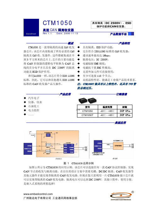
CTM1050广州致远电子有限公司 工业通讯网络事业部———————————————概述CTM1050是一款带隔离的高速CAN 收发器芯片,该芯片内部集成了所有必需的CAN 隔离及CAN 收、发器件,这些都被集成在不到3平方厘米的芯片上。
芯片的主要功能是将CAN 控制器的逻辑电平转换为CAN 总线的差分电平并且具有DC 2500V 的隔离功能及ESD 保护作用。
和TJA1050一样,该芯片符合ISO 11898标准,因此,它可以和其他遵从ISO 11898标准的CAN 收发器产品互操作。
——————————————产品特性 具有隔离、ESD 保护功能;完全符合ISO11898标准的CAN 收发器; 通讯速率最高达1Mbps; 隔离电压:DC 2500V; 电磁辐射EME 极低; 电磁抗干扰EMI 性极高; 无需外加元件可直接使用; 至少可连接110个节点;高低温特性好,能满足工业级产品技术要求。
注:CTM1050T 除具有以上特性外,还具有TVS 管 防总线过压。
————————————产品应用 ◆ 汽车电子 ◆ 仪器、仪表 ◆ 石油化工 ◆ 电力监控 ◆ ……—————————————订购信息型号温度范围 封装CTM1050 -40℃—+85℃ DIP-8Pin CTM1050T-40℃—+85℃DIP-8Pin————————————————————————————————典型应用图 1 CTM1050应用示例如图1所示为CTM1050的应用示例,该芯片可以连接任何一款CAN 协议控制器,实现CAN 节点的收发与隔离功能。
在以往的设计方案中需要光耦、DC/DC 隔离、CAN 收发器等其他元器件才能实现带隔离的CAN 收发电路,但现在您只需利用一片CTM1050接口芯片就可以实现带隔离的CAN 收发电路,隔离电压可以达到DC 2500V ,其接口简单,使用方便,是嵌入式系统的理想选择!共享修订历史版本日期原因Rev X1 2006/6/8 内部制定初稿Rev 1.0 2006/6/16 第一次发布Rev 1.1 2006/11/11 数据手册升级共享目录销售信息 (2)技术支持 (2)1. 功能简介 (3)2. 引脚信息 (4)2.1 CTM1050引脚信息 (4)3. CTM1050特性参数 (5)3.1 参数列表 (5)3.2 电气特性 (5)3.3 绝缘特性 (6)4. 机械尺寸 (7)4.1 CTM1050机械尺寸 (7)5. 电路连接 (8)5.1 CTM1050电路连接 (8)6. 声明 (9)共享销售信息如果需要购买本产品,请在办公时间(星期一至五上午8:30~11:50;下午1:30~5:30;星期六上午8:30~11:50)拨打电话咨询广州致远电子有限公司。
STA1050中文资料

Digital Servo
■ Automatic fine gain/balance/offset adjustment for tracking and focus
■ Embedded 16bit servo DSP (33.8688MHz) with programmable sampling rate
2
Pin function description . . . . . . . . . . . . . . . . . . . . . . . . . . . . . . . . . . . . . . 4
3
System description . . . . . . . . . . . . . . . . . . . . . . . . . . . . . . . . . . . . . . . . . . 8
fade/
mute/ deemph
+
3/11
A
B
C
D
I/V OFFSET GAIN ADC
E
F
DAC ANALOG PLL filter
1.7Kx32 PRAM DSP
A+C B+D E F 256x16 XRAM
A+C
DECIM. TrackCount 256x16 YRAM
B+D
+ JumpSpeed
2/11
元器件交易网
STA1050
1
Block diagram
Figure 1. Block diagram
master clock
TJA1050中文资料_数据手册_参数

2003年10月22日 4飞利浦半导体产品SPECI FI CATION高速CAN收发器 TJA1050功能说明 TJA1050是CAN协议之间的接口控制器和物理 总线.它主要用于使用波特率的高速汽车应用 60 KBAUD到1 MBAUD.它提供差分传输总线能力和差分接收器能力 CAN协议控制器.它完 全兼容 “ISO 11898”标准.限流电路保护发射机输出阶段由意外短路造成的损坏虽然电力正常或负电源电压在这种故障状态下功耗会 增加.热保护电路可保护IC免受损坏通过关闭发射机如果结温超过约165的值 C.因为发射机消耗大部分功率和功率 IC的耗散和温度降 低.所有其他 IC功能继续运行.发射机关闭状态当引脚TXD变为高电平时复位.热保护当总线短路时尤其需要电路. CANH和CANL引脚不 受汽车的保护电瞬变(根据 “ISO 7637”;参见图4).控制引脚S允许选择两种工作模式:高速模式或静音模式.高速模式是正常的操作 模式,并且是通过将引脚S连接到地面来选择.这是默认设置模式,如果引脚S未连接.但是,要确保EMI在仅使用高速应用的应用中表现 出色模式,建议将引脚S连接到地面.在静音模式下,发射器被禁用.所有其他 IC功能继续运行.无声模式是 通过连接引脚S到V CC进行 选择 ,可用于防止网络通信被阻塞,到期到一个失控的CAN控制器. “TXD主导超时”定时器电路阻止总线线路被驱动到永久主导状 态(阻塞)所有网络通信)如果引脚TXD被强制由硬件和/或软件永久为低应用失败.定时器由否定触发边沿TXD引脚.如果持续低电平 的话 TXD引脚超过内部定时器值,发送器为残疾,驾驶巴士进入隐性状态.定时器由引脚TXD上的上升沿复位.表格1 CAN收发器的功 能表; X =不在乎 V CC TXD小号 CANH CANL总线状态 RXD 4.75 V至5.25 V低低(或 FL替罪羊)高低优势低 4.75 V至5.25 V X高 0.5V CC 0.5V CC隐性高 4.75 V至5.25 V高( 飞利浦半导体产品SPECI FI CATION高速CAN收发器 TJA1050手册,全页面宽度 50 80 0 020三十 10 MGT231 40 F(MHZ) 20 40 60一个 (D B μV)图9高达50 MHZ的典型电磁发射(峰值幅度测量).数据速率为500千比特/秒.手册,全页面宽度 10 80 0 04 6 2 MGT233 8 F(MHZ) 20 40 60一个 (D B μV)图10高达10 MHZ的典型电磁发射(峰值幅度测量和峰值包络振幅).数据速率为500千比特/秒. 图1方框图.钉扎符号销描述 TXD 1传输数据输入;读入数据从CAN控制器到总线线路司机 GND 2地面 V CC 3电源电压 RXD 4接收数据输 出;读出来从公交线路到公交车的数据 CAN控制器 V REF五参考电压输出 CANL 6低级CAN总线 CANH 7高级CAN总线小号 8选择高速 模式的输入或静音模式手册,HALFPAGE 1 2 3 4 8 7 6五 MGS375 TJA1050T小号 CANH GND CANL VREF RXD VCC TXD图2引脚配置
电子元器件zdt1053中文资料_数据手册_IC数据表
Cobo ton toff
21
30
pF
VCB=10V, f=1MHz
90
ns
IC=2A, IB=20mA, VCC=50V
750
ns
IC=2A, IB=±20mA, VCC=50V
*Measured under pulsed conditions. Pulse width=300µs. Duty cycle ≤2%
55.6
°C/ W
45.5
°C/ W
* The power which can be dissipated assuming the device is mounted in a typical manner on a PCB with copper equal to 2 inches square.
Cobo ton toff
21
30
pF
VCB=10V, f=1MHz
90
ns
IC=2A, IB=20mA, VCC=50V
750
ns
IC=2A, IB=±20mA, VCC=50V
*Measured under pulsed conditions. Pulse width=300µs. Duty cycle ≤2%
1200
150
220
30
50
15
IC=10mA, VCE=2V* IC=1A, VCE=2V* IC=2A, VCE=2V* IC=5A, VCE=2V* IC=10A, VCE=2V*
140
MHz
IC=50mA, VCE=10V
f=100MHz
Output Capacitance Switching Times
tja1050中文资料

1 接口电路设计中的关键问题1.1光电隔离电路光电隔离电路虽然能增强系统的抗干扰能力,但也会增加CAN总线有效回路信号的传输延迟时间,导致通信速率或距离减少。
82C250等型号的CAN收发器本身具备瞬间抗干扰、降低射频干扰(RFI)以及实现热防护的能力,其具有的电流限制电路还提供了对总线的进一步保护功能。
因此,如果现场传输距离近、电磁干扰小,可以不采用光电隔离,以使系统达到最大的通信速率或距离,并且可以简化接口电路。
如果现场环境需要光电隔离,应选用高速光电隔离器件,以减少CAN总线有效回路信号的传输延迟时间,如高速光电耦合器6N137,传输延迟时间短,典型值仅为48 ns,已接近TTL电路传输延迟时间的水平。
1.2 电源隔离光电隔离器件两侧所用电源Vdd与Vcc必须完全隔离,否则,光电隔离将失去应有的作用。
电源的隔离可通过小功率DC/DC电源隔离模块实现,如外形尺寸为DIP-14标准脚位的5 V 双路隔离输出的小功率DC/DC模块。
1.3 上拉电阻图1中的CAN收发器82C250的发送数据输入端TXD与光电耦合器6N137的输出端OUT相连,注意TXD必须同时接上拉电阻R3。
一方面,R3保证6N137中的光敏三极管导通时输出低电平,截止时输出高电平;另一方面,这也是CAN 总线的要求。
具体而言,82C250的TXD端的状态决定着高、低电平CAN 电压输入/输出端CANH、CANL的状态(见表1)。
CAN总线规定,总线在空闲期间应呈隐性,即CAN 网络中节点的缺省状态是隐性,这要求82C25O 的TXD端的缺省状态为逻辑1(高电平)。
为此,必须通过R3确保在不发送数据或出现异常情况时,TXD端的状态为逻辑1(高电平)。
1.4总线阻抗匹配CAN总线的末端必须连接2个120Ω的电阻,它们对总线阻抗匹配有着重要的作用,不可省略。
否则,将大大降低总线数据通信时的可靠性和抗干扰性,甚至有可能导致无法通信。
1.5 其它抗干扰措施为提高接口电路的抗干扰能力,还可考虑以下措施:(1)在82C25O的CANH、CANL端与地之间并联2个30 pF的小电容,以滤除总线上的高频干扰,防止电磁辐射。
- 1、下载文档前请自行甄别文档内容的完整性,平台不提供额外的编辑、内容补充、找答案等附加服务。
- 2、"仅部分预览"的文档,不可在线预览部分如存在完整性等问题,可反馈申请退款(可完整预览的文档不适用该条件!)。
- 3、如文档侵犯您的权益,请联系客服反馈,我们会尽快为您处理(人工客服工作时间:9:00-18:30)。
ZXCT1050Precision wide input range current monitorDescriptionOrdering informationThe ZXCT1050 is a wide input range current monitor, which operates over a range of input voltages from ground up to V CC -2V. As a result the ZXCT1050 can be used on the high or low side of the load.The ZXCT1050 provides variable gain by using two external resistors. The first of which sets the transconductance and the second setting the overall gain.The very low offset voltage enables a typical accuracy of 1% for sense voltages of only 30mV,giving better tolerances for small sense resistors necessary at higher currents.Features•Accurate down to end current sensing •Output voltage scaling x10•0 to V CC -2V sense input range • 2.7 to 20V supply range •50µA quiescent current •SOT23-5 packageApplications•Power supply•DC motor and solenoid control •Battery management •Over current monitor •Power management •Short circuit detectionPin connectionsTypical application circuitOrder code Pack Part mark Reel size(inches)Tape width (mm)Quantity per reel ZXCT1050E5TASOT23-51050783000Absolute maximum ratingsV CC max.20V Voltage on SENSE- and SENSE+-0.6 to V CCVoltage on all other pins -0.6V and V CC +0.6V V SENSE = ‘(V SENSE +) - (V SENSE -)’500mV Operating temperature -40 to 125°C Storage temperature-55 to 150°C Maximum junction temperature 150°CPackage power dissipation300mW * at T A = 25°C (De-rate to zero for T J = 150°C)Operation above the absolute maximum rating may cause device failure. Operation at the absolute maximum ratings, for extended periods, may reduce device reliability.Recommended operating conditionsRecommended resistor gain setting combinationsPin function tableParameterMin.Max.Units V SENSE+Common-mode sense input range 0V CC -2V V CC Supply voltage range2.720V V SENSE Differential sense input voltage range 10300mV V OUTOutput voltage range 0V CC -2V T AAmbient temperature range-40125°CGain R SH R G 107.5k ⍀ 3.75k ⍀207.5k ⍀7.5k ⍀507.5k ⍀18.7k ⍀1007.5k ⍀37.5k ⍀20 3.75k ⍀ 3.75k ⍀50 1.5k ⍀ 3.75k ⍀100750⍀3.75k ⍀PIN Name Description1V CC This is the analog supply and provides power to internal circuitry.2GND Ground pin.3OUT Output pin. A resistor, R GAIN , connected from this pin pin down to ground develops an output voltage.4SENSE+This is the positive input of the current monitor and has an input range from 0V up to V CC – 2V.5SENSE-This is the negative input of the current monitor and has an input range from 0V up to V CC – 2V. The current through this pin varies with differential sense voltage. A resistor, R SHUNT , from this pin to the rail being sensed set the transconductance of the current monitor.Electrical characteristicsTest conditions T A = 25°C, V SENSE+ = 10V, V CC = 12V, V SENSE = 100mV, R SH = 7.5k ⍀, R G = 3.75k ⍀.SymbolParameter Conditions Min.Typ.Max.Units I Q V CC pin current V SENSE = 0V 4570µA V OUTOutput voltageV SENSE = 0V =30mV =100mV =150mV02850.971.4533001.001.50153151.031.55mVmV V V I SENSE+V SENSE+ input current V SENSE = 0V 60150nA I SENSE-V SENSE- input current V SENSE = 0V 15150nA V OUT TC V OUT variation with temperature See note (*)NOTES:(*)Temperature dependent measurements are extracted from characterisation and simulation results.300ppm/°CGain V OUT /V SENSE 10Accuracy Total output error -33%BWBandwidthV SENSE(DC) = 10mV V SENSE(AC) = 10mV PPCL = 5pF , 300kHz VSENSE(DC)= 100mV0.8MHz PSRR Power supply rejection ratio V CC = 2.7V to 20V V SENSE+ = 0.7V 60dB CMRRCommon mode rejection ratioV CC = 20VV SENSE+ = 0 to 18V70dBTypical characteristicsR G = 3.75k⍀, R SH = 7.5k⍀ unless otherwise stated.Typical characteristicsR G = 3.75k⍀, R SH = 7.5k⍀ unless otherwise stated.Typical characteristicsR G = 3.75k⍀, R SH = 7.5k⍀ unless otherwise stated.Applications informationThe ZXCT1050 is a current output version of the ZXCT1051 and as such uses a separate power supply pin. All biasing for the internal amplifiers comes from its separate V CC input and is not ‘line powered’, unlike the ZXCT1021.This means that at very small sense voltages the ZXCT1050 draws very little current (<1A) from the lines being sensed.The separate V CC pin enables the ZXCT1050 to be operated at sense line voltages down to 0V,where the ZXCT1021 would switch off. This feature enables the ZXCT1050 to be used to sense the currents flowing through lines that have been shorted to ground.Basic operationLoad current, I L , from V RAIL is drawn through R SENSE developing a voltage V SENSE across the sense inputs of the ZXCT1050.The internal amplifier forces V SENSE across external resistance R SH (internal on the ZXCT1051)causing a current to flow through transistor Q1 and out of the output pin, OUT. This current is then converted to a voltage by a resistor, R G , between OUT and GND.The overall gain of the ZXCT1050 is determined by the following expression:A ratio of 1:2 between R SH and R G creates the fixed gain of 10 with an output impedance equal to RG (see electrical characteristics for output current-voltage characteristics).The ZXCT1050 has both R G and R SH external. This allows R G and R SH to be varied so that the required gain can be achieved at the required output impedance.For low power applications both R G and R SH can be increased whereas for driving low impedance R G and R SH can be decreased.The maximum recommended value for R G is 40k ⍀ and the maximum recommended value for RSH is 10k ⍀. Large values of R SH start increasing the effective input offset error, while large values of R G can created load errors and reduce bandwidths.The maximum differential input voltage, V SENSE , is 150mV (I L * R SENSE ); however voltages up to 500mV will not damage it. This can be increased further by the inclusion of a resistor, R LIM ,between the SENSE+ pin and the rail being sensed, V RAIL .For best performance R SENSE should be connected as close to the SENSE+ and SENSE- pins thus minimizing any series resistance with R SENSE .GAIN 20R GR SH----------×=Package outline - SOT23-5Note: Controlling dimensions are in millimeters. Approximate dimensions are provided in inchesDIM MillimetersInchesMin.Max.Min.Max.A - 1.00-0.0393A10.010.100.00030.0039A20.840.900.03300.0354b 0.300.450.01180.0177c 0.120.200.00470.0078D 2.90 BSC 0.114 BSCE 2.80 BSC 0.110 BSC E1 1.60 BSC 0.062 BSC e 0.95 BSC 0.0374 BSC e1 1.90 BSC0.0748 BSCL 0.300.500.01180.0196L20.25 BSC 0.010 BSCa°4°12°4°12°DefinitionsProduct changeZetex Semiconductors reserves the right to alter, without notice, specifications, design, price or conditions of supply of any product or service. Customers are solely responsible for obtaining the latest relevant information before placing orders.Applications disclaimerThe circuits in this design/application note are offered as design ideas. It is the responsibility of the user to ensure that the circuit is fit for the user’s application and meets with the user’s requirements. No representation or warranty is given and no liability whatsoever is assumed by Zetex with respect to the accuracy or use of such information, or infringement of patents or other intellectual property rights arising from such use or otherwise. Zetex does not assume any legal responsibility or will not be held legally liable (whether in contract, tort (including negligence), breach of statutory duty, restriction or otherwise) for any damages, loss of profit, business, contract, opportunity or consequential loss in the use of these circuit applications, under any circumstances.Life supportZetex products are specifically not authorized for use as critical components in life support devices or systems without the express written approval of the Chief Executive Officer of Zetex Semiconductors plc. As used herein:A. Life support devices or systems are devices or systems which:1.are intended to implant into the bodyor2.support or sustain life and whose failure to perform when properly used in accordance with instructions for use provided in thelabelling can be reasonably expected to result in significant injury to the user.B. A critical component is any component in a life support device or system whose failure to perform can be reasonably expected tocause the failure of the life support device or to affect its safety or effectiveness.ReproductionThe product specifications contained in this publication are issued to provide outline information only which (unless agreed by the company in writing) may not be used, applied or reproduced for any purpose or form part of any order or contract or be regarded as a representation relating to the products or services concerned.Terms and ConditionsAll products are sold subjects to Zetex’ terms and conditions of sale, and this disclaimer (save in the event of a conflict between the two when the terms of the contract shall prevail) according to region, supplied at the time of order acknowledgement.For the latest information on technology, delivery terms and conditions and prices, please contact your nearest Zetex sales office.Quality of productZetex is an ISO 9001 and TS16949 certified semiconductor manufacturer.To ensure quality of service and products we strongly advise the purchase of parts directly from Zetex Semiconductors or one of our regionally authorized distributors. For a complete listing of authorized distributors please visit: /salesnetworkZetex Semiconductors does not warrant or accept any liability whatsoever in respect of any parts purchased through unauthorized sales channels. ESD(Electrostatic discharge)Semiconductor devices are susceptible to damage by ESD. Suitable precautions should be taken when handling and transporting devices. The possible damage to devices depends on the circumstances of the handling and transporting, and the nature of the device. The extent of damage can vary from immediate functional or parametric malfunction to degradation of function or performance in use over time. Devices suspected of being affected should be replaced.Green complianceZetex Semiconductors is committed to environmental excellence in all aspects of its operations which includes meeting or exceeding regulatory requirements with respect to the use of hazardous substances. Numerous successful programs have been implemented to reduce the use of hazardous substances and/or emissions.All Zetex components are compliant with the RoHS directive, and through this it is supporting its customers in their compliance with WEEE and ELV directives.Product status key:“Preview”Future device intended for production at some point. Samples may be available“Active”Product status recommended for new designs“Last time buy (LTB)”Device will be discontinued and last time buy period and delivery is in effect“Not recommended for new designs”Device is still in production to support existing designs and production“Obsolete”Production has been discontinuedDatasheet status key:“Draft version”This term denotes a very early datasheet version and contains highly provisional information, whichmay change in any manner without notice.“Provisional version”This term denotes a pre-release datasheet. It provides a clear indication of anticipated performance.However, changes to the test conditions and specifications may occur, at any time and without notice.“Issue”This term denotes an issued datasheet containing finalized specifications. However, changes tospecifications may occur, at any time and without notice.。