Ti(德州仪器)-芯片手册-sn74ac86
SN74LS86N中文资料
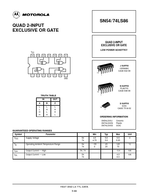
SN54/74LS86 QUAD 2-INPUT EXCLUSIVE OR GATE
QUAD 2-INPUT EXCLUSIVE OR GATE
LOW POWER SCHOTTKY
VCC 14 13 12 11 10 9 8
J SUFFIX CERAMIC CASE 632-08
GUARANTEED OPERATING RANGES
Symbol VCC TA IOH IOL Supply Voltage Operating Ambient Temperature Range Output Current — High Output Current — Low Parameter 54 74 54 74 54, 74 54 74 Min 4.5 4.75 – 55 0 Typ 5.0 5.0 25 25 Max 5.5 5.25 125 70 – 0.4 4.0 8.0 Unit V °C mA mA
FAST AND LS TTL DATA 5-89
14
1
2
3
4
6
7 GND
1
14
N SUFFIX PLASTIC CASE 646-06
1
TRUTH TABLE
IN A L L H H B L H L H OUT Z L H H L
14 1
D SUFFIX SOIC CASE 751A-02
ORDERING INFORMATION
SN54LSXXJ SN74LSXXN SN74LSXXD Ceramic Plastic SOIC
VCC = MAX, VIN = 2.7 V VCC = MAX, VIN = 7.0 V VCC = MAX, VIN = 0.4 V VCC = MAX VCC = MAX
ST M74HC86 数据手册

1/8July 2001sHIGH SPEED:t PD = 12ns (TYP .) at V CC = 6V sLOW POWER DISSIPATION:I CC = 1µA(MAX.) at T A =25°C sHIGH NOISE IMMUNITY:V NIH = V NIL = 28 % V CC (MIN.)sSYMMETRICAL OUTPUT IMPEDANCE:|I OH | = I OL = 4mA (MIN)sBALANCED PROPAGATION DELAYS:t PLH ≅ t PHLsWIDE OPERATING VOLTAGE RANGE:V CC (OPR) = 2V to 6VsPIN AND FUNCTION COMPATIBLE WITH 74 SERIES 86DESCRIPTIONThe M74HC86 is an high speed CMOS QUAD EXCLUSIVE OR GATE fabricated with silicon gate C 2MOS technology.Input and output buffer are installed, which enables high noise immunity and stable output.All inputs are equipped with protection circuits against static discharge and transient excess voltage.M74HC86QUAD EXCLUSIVE OR GATEPIN CONNECTION AND IEC LOGIC SYMBOLSORDER CODESPACKAGE TUBE T & R DIP M74HC86B1R SOP M74HC86M1RM74HC86RM13TR TSSOPM74HC86TTRM74HC862/8INPUT AND OUTPUT EQUIVALENT CIRCUITPIN DESCRIPTIONTRUTH TABLEABSOLUTE MAXIMUM RATINGSAbsolute Maximum Ratings are those values beyond which damage to the device may occur. Functional operation under these conditions is not implied(*) 500mW at 65 °C; derate to 300mW by 10mW/°C from 65°C to 85°CRECOMMENDED OPERATING CONDITIONSPIN No SYMBOL NAME AND FUNCTION 1, 4, 9, 121A to 4A Data Inputs 2, 5, 10, 131B to 4B Data Inputs 3, 6, 8, 111Y to 4Y Data Outputs 7GND Ground (0V)14V CCPositive Supply VoltageA B Y L L L L H H H L H HHLSymbol ParameterValue Unit V CC Supply Voltage -0.5 to +7V V I DC Input Voltage -0.5 to V CC + 0.5V V O DC Output Voltage -0.5 to V CC + 0.5V I IK DC Input Diode Current ± 20mA I OK DC Output Diode Current ± 20mA I ODC Output Current± 25mA I CC or I GND DC V CC or Ground Current± 50mA P D Power Dissipation500(*)mW T stg Storage Temperature -65 to +150°C T LLead Temperature (10 sec)300°CSymbol ParameterValue Unit V CC Supply Voltage 2 to 6V V I Input Voltage 0 to V CC V V O Output Voltage 0 to V CC V T op Operating Temperature -55 to 125°C t r , t fInput Rise and Fall TimeV CC = 2.0V 0 to 1000ns V CC = 4.5V 0 to 500ns V CC = 6.0V0 to 400nsM74HC863/8DC SPECIFICATIONSAC ELECTRICAL CHARACTERISTICS (C L = 50 pF, Input t r = t f = 6ns)CAPACITIVE CHARACTERISTICS1) C PD is defined as the value of the IC’s internal equivalent capacitance which is calculated from the operating current consumption without load. (Refer to Test Circuit). Average operating current can be obtained by the following equation. I CC(opr) = C PD x V CC x f IN + I CC /4 (per gate)SymbolParameterTest ConditionValue UnitV CC (V)T A = 25°C -40 to 85°C -55 to 125°C Min.Typ.Max.Min.Max.Min.Max.V IHHigh Level Input Voltage2.0 1.5 1.5 1.5V 4.53.15 3.15 3.156.04.24.24.2V ILLow Level Input Voltage2.00.50.50.5V4.5 1.35 1.35 1.356.0 1.81.81.8V OHHigh Level Output Voltage2.0I O =-20 µA 1.9 2.0 1.9 1.9V4.5I O =-20 µA 4.4 4.5 4.4 4.46.0I O =-20 µA5.96.0 5.9 5.94.5I O =-4.0 mA 4.18 4.31 4.13 4.106.0I O =-5.2 mA 5.685.8 5.635.60V OLLow Level Output Voltage2.0I O =20 µA 0.00.10.10.1V 4.5I O =20 µA 0.00.10.10.16.0I O =20 µA 0.00.10.10.14.5I O =4.0 mA 0.170.260.330.406.0I O =5.2 mA 0.180.260.330.40I I Input Leakage Current6.0V I = V CC or GND ± 0.1± 1± 1µA I CCQuiescent Supply Current6.0V I = V CC or GND11020µA SymbolParameterTest ConditionValue UnitV CC (V)T A = 25°C -40 to 85°C -55 to 125°C Min.Typ.Max.Min.Max.Min.Max.t TLH t THL Output TransitionTime 2.0307595110ns 4.581519226.07131619t PLH t PHL Propagation DelayTime2.0561********ns4.5142228336.012192428SymbolParameterTest ConditionValue UnitV CC (V)T A = 25°C -40 to 85°C -55 to 125°C Min.Typ.Max.Min.Max.Min.Max.C IN Input Capacitance 5.05101010pF C PDPower Dissipation Capacitance (note 1)5.026pFM74HC864/8TEST CIRCUITL R T = Z OUT of pulse generator (typically 50Ω)WAVEFORM : PROPAGATION DELAY TIME(f=1MHz; 50% duty cycle)M74HC86Information furnished is believed to be accurate and reliable. However, STMicroelectronics assumes no responsibility for the consequences of use of such information nor for any infringement of patents or other rights of third parties which may result from its use. No license is granted by implication or otherwise under any patent or patent rights of STMicroelectronics. Specifications mentioned in this publication are subject to change without notice. This publication supersedes and replaces all information previously supplied. STMicroelectronics products are not authorized for use as critical components in life support devices or systems without express written approval of STMicroelectronics.© The ST logo is a registered trademark of STMicroelectronics© 2001 STMicroelectronics - Printed in Italy - All Rights ReservedSTMicroelectronics GROUP OF COMPANIESAustralia - Brazil - China - Finland - France - Germany - Hong Kong - India - Italy - Japan - Malaysia - Malta - MoroccoSingapore - Spain - Sweden - Switzerland - United Kingdom© 8/8。
CD74AC86中文资料

0.05
3
0.05
4.5
12
3
24
4.5
75
5.5
(Note 6, 7)
50
5.5
(Note 6, 7)
25oC MIN MAX
-40oC TO 85oC
MIN MAX
-55oC TO 125oC
MIN MAX
UNITS
1.2
-
1.2
-
1.2
-
V
2.1
-
2.1
-
2.1
-
V
3.85
-
3.85
-
3.85
DC Electrical Specifications
PARAMETER AC TYPES High Level Input Voltage Low Level Input Voltage High Level Output Voltage
Low Level Output Voltage
TEST
CONDITIONS
• Speed of Bipolar FAST™/AS/S with Significantly Reduced Power Consumption
• Balanced Propagation Delays
• AC Types Feature 1.5V to 5.5V Operation and Balanced Noise Immunity at 30% of the Supply
CD54ACT86F3A CD74ACT86E
CD74ACT86M
-55 to 125
0 to 70oC, -40 to 85, -55 to 125
0 to 70oC, -40 to 85, -55 to 125
SN74LS86中文资料

LOW POWER SCHOTTKYDevice Package Shipping SN74LS86N 14 Pin DIP 2000 Units/Box SN74LS86D14 PinSOIC D SUFFIX CASE 751A2500/T ape & ReelPLASTIC N SUFFIX CASE 646141141ON Semiconductor and are trademarks of Semiconductor Components Industries, LLC (SCILLC). SCILLC reserves the right to make changes without further notice to any products herein. SCILLC makes no warranty, representation or guarantee regarding the suitability of its products for any particular purpose, nor does SCILLC assume any liability arising out of the application or use of any product or circuit, and specifically disclaims any and all liability, including without limitation special, consequential or incidental damages. “Typical” parameters which may be provided in SCILLC data sheets and/or specifications can and do vary in different applications and actual performance may vary over time. All operating parameters, including “Typicals” must be validated for each customer application by customer’s technical experts. SCILLC does not convey any license under its patent rights nor the rights of others.SCILLC products are not designed, intended, or authorized for use as components in systems intended for surgical implant into the body, or other applications intended to support or sustain life, or for any other application in which the failure of the SCILLC product could create a situation where personal injury or death may occur. Should Buyer purchase or use SCILLC products for any such unintended or unauthorized application, Buyer shall indemnify and hold SCILLC and its officers, employees, subsidiaries, affiliates, and distributors harmless against all claims, costs, damages, and expenses, and reasonable attorney fees arising out of, directly or indirectly, any claim of personal injury or death associated with such unintended or unauthorized use, even if such claim alleges that SCILLC was negligent regarding the design or manufacture of the part. SCILLC is an Equal Opportunity/Affirmative Action Employer. PUBLICATION ORDERING INFORMATIONASIA/PACIFIC: LDC for ON Semiconductor – Asia SupportPhone:303–675–2121 (Tue–Fri 9:00am to 1:00pm, Hong Kong Time)Toll Free from Hong Kong 800–4422–3781Email: ONlit–asia@JAPAN: ON Semiconductor, Japan Customer Focus Center4–32–1 Nishi–Gotanda, Shinagawa–ku, Tokyo, Japan 141–8549Phone: 81–3–5487–8345Email: r14153@Fax Response Line:303–675–2167。
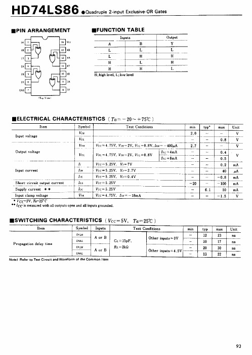
74ls86中文资料_数据手册_参数
Singapore 049318
Harbour City, Canton Road, Tsim Sha Tsui,
Tel: 535-2100
Kowloon, Hong Kong
Fax: 535-1533
Tel: <852> (2) 735 9218
Fax: <852> (2) 730 0281
Hitachi Asia Ltd.
Hitachi Europe GmbH Electronic components Group Dornacher Stra§e 3 D-85622 Feldkirchen, Munich Germany Tel: <49> (89) 9 9180-0 Fax: <49> (89) 9 29 30 00
DP-14 Conforms Conforms 0.97 g
10.06 10.5 Max
14
8
5.5
1
7
1.42 Max
0.10 ± 0.10
1.27
*0.42 ± 0.08 0.40 ± 0.06
0.15 0.12 M
*Dimension including the plating thickness Base material dimension
For further information write to:
74系列芯片功能大全

74系列芯片功能大全同型号的74系列、74HC系列、74LS系列芯片,逻辑功能上是一样的。
74LSxx、74HCxx的使用说明可参阅74xx的使用说明。
有些型号里包含了几种型号,如74HC161资料里包含了74HC160、74HC161、74HC162、74HC163四种芯片的功能。
7400 TTL 2输入端四与非门7401 TTL 集电极开路2输入端四与非门7402 TTL 2输入端四或非门7403 TTL 集电极开路2输入端四与非门7404 TTL 六反相器7405 TTL 集电极开路六反相器7406 TTL 集电极开路六反相高压驱动器7407 TTL 集电极开路六正相高压驱动器7408 TTL 2输入端四与门7409 TTL 集电极开路2输入端四与门7410 TTL 3输入端3与非门74107 TTL 带清除主从双J-K触发器74109 TTL 带预置清除正触发双J-K触发器7411 TTL 3输入端3与门74112 TTL 带预置清除负触发双J-K触发器7412 TTL 开路输出3输入端三与非门74121 TTL 单稳态多谐振荡器74122 TTL 可再触发单稳态多谐振荡器74123 TTL 双可再触发单稳态多谐振荡器74125 TTL 三态输出高有效四总线缓冲门74126 TTL 三态输出低有效四总线缓冲门7413 TTL 4输入端双与非施密特触发器74132 TTL 2输入端四与非施密特触发器74133 TTL 13输入端与非门74136 TTL 四异或门74138 TTL 3-8线译码器/复工器74139 TTL 双2-4线译码器/复工器7414 TTL 六反相施密特触发器74145 TTL BCD—十进制译码/驱动器7415 TTL 开路输出3输入端三与门74150 TTL 16选1数据选择/多路开关74151 TTL 8选1数据选择器74153 TTL 双4选1数据选择器74154 TTL 4线—16线译码器74155 TTL 图腾柱输出译码器/分配器74156 TTL 开路输出译码器/分配器74157 TTL 同相输出四2选1数据选择器74158 TTL 反相输出四2选1数据选择器7416 TTL 开路输出六反相缓冲/驱动器74160 TTL 可预置BCD异步清除计数器74161 TTL 可予制四位二进制异步清除计数器74162 TTL 可预置BCD同步清除计数器74163 TTL 可予制四位二进制同步清除计数器74164 TTL 八位串行入/并行输出移位寄存器74165 TTL 八位并行入/串行输出移位寄存器74166 TTL 八位并入/串出移位寄存器74169 TTL 二进制四位加/减同步计数器7417 TTL 开路输出六同相缓冲/驱动器74170 TTL 开路输出4×4寄存器堆74173 TTL 三态输出四位D型寄存器74174 TTL 带公共时钟和复位六D触发器74175 TTL 带公共时钟和复位四D触发器74180 TTL 9位奇数/偶数发生器/校验器74181 TTL 算术逻辑单元/函数发生器74185 TTL 二进制—BCD代码转换器74190 TTL BCD同步加/减计数器74191 TTL 二进制同步可逆计数器74192 TTL 可预置BCD双时钟可逆计数器74193 TTL 可预置四位二进制双时钟可逆计数器74194 TTL 四位双向通用移位寄存器74195 TTL 四位并行通道移位寄存器74196 TTL 十进制/二-十进制可预置计数锁存器74197 TTL 二进制可预置锁存器/计数器7420 TTL 4输入端双与非门7421 TTL 4输入端双与门7422 TTL 开路输出4输入端双与非门74221 TTL 双/单稳态多谐振荡器74240 TTL 八反相三态缓冲器/线驱动器74241 TTL 八同相三态缓冲器/线驱动器74243 TTL 四同相三态总线收发器74244 TTL 八同相三态缓冲器/线驱动器74245 TTL 八同相三态总线收发器74247 TTL BCD—7段15V输出译码/驱动器74248 TTL BCD—7段译码/升压输出驱动器74249 TTL BCD—7段译码/开路输出驱动器74251 TTL 三态输出8选1数据选择器/复工器74253 TTL 三态输出双4选1数据选择器/复工器74256 TTL 双四位可寻址锁存器74257 TTL 三态原码四2选1数据选择器/复工器74258 TTL 三态反码四2选1数据选择器/复工器74259 TTL 八位可寻址锁存器/3-8线译码器7426 TTL 2输入端高压接口四与非门74260 TTL 5输入端双或非门74266 TTL 2输入端四异或非门7427 TTL 3输入端三或非门74273 TTL 带公共时钟复位八D触发器74279 TTL 四图腾柱输出S-R锁存器7428 TTL 2输入端四或非门缓冲器74283 TTL 4位二进制全加器74290 TTL 二/五分频十进制计数器74293 TTL 二/八分频四位二进制计数器74295 TTL 四位双向通用移位寄存器74298 TTL 四2输入多路带存贮开关74299 TTL 三态输出八位通用移位寄存器7430 TTL 8输入端与非门7432 TTL 2输入端四或门74322 TTL 带符号扩展端八位移位寄存器74323 TTL 三态输出八位双向移位/存贮寄存器7433 TTL 开路输出2输入端四或非缓冲器74347 TTL BCD—7段译码器/驱动器74352 TTL 双4选1数据选择器/复工器74353 TTL 三态输出双4选1数据选择器/复工器74365 TTL 门使能输入三态输出六同相线驱动器74365 TTL 门使能输入三态输出六同相线驱动器74366 TTL 门使能输入三态输出六反相线驱动器74367 TTL 4/2线使能输入三态六同相线驱动器74368 TTL 4/2线使能输入三态六反相线驱动器7437 TTL 开路输出2输入端四与非缓冲器74373 TTL 三态同相八D锁存器74374 TTL 三态反相八D锁存器74375 TTL 4位双稳态锁存器74377 TTL 单边输出公共使能八D锁存器74378 TTL 单边输出公共使能六D锁存器74379 TTL 双边输出公共使能四D锁存器7438 TTL 开路输出2输入端四与非缓冲器74380 TTL 多功能八进制寄存器7439 TTL 开路输出2输入端四与非缓冲器74390 TTL 双十进制计数器74393 TTL 双四位二进制计数器7440 TTL 4输入端双与非缓冲器7442 TTL BCD—十进制代码转换器74352 TTL 双4选1数据选择器/复工器74353 TTL 三态输出双4选1数据选择器/复工器74365 TTL 门使能输入三态输出六同相线驱动器74366 TTL 门使能输入三态输出六反相线驱动器74367 TTL 4/2线使能输入三态六同相线驱动器74368 TTL 4/2线使能输入三态六反相线驱动器7437 TTL 开路输出2输入端四与非缓冲器74373 TTL 三态同相八D锁存器74374 TTL 三态反相八D锁存器74375 TTL 4位双稳态锁存器74377 TTL 单边输出公共使能八D锁存器74378 TTL 单边输出公共使能六D锁存器74379 TTL 双边输出公共使能四D锁存器7438 TTL 开路输出2输入端四与非缓冲器74380 TTL 多功能八进制寄存器7439 TTL 开路输出2输入端四与非缓冲器74390 TTL 双十进制计数器74393 TTL 双四位二进制计数器7440 TTL 4输入端双与非缓冲器7442 TTL BCD—十进制代码转换器74447 TTL BCD—7段译码器/驱动器7445 TTL BCD—十进制代码转换/驱动器74450 TTL 16:1多路转接复用器多工器74451 TTL 双8:1多路转接复用器多工器74453 TTL 四4:1多路转接复用器多工器7446 TTL BCD—7段低有效译码/驱动器74460 TTL 十位比较器74461 TTL 八进制计数器74465 TTL 三态同相2与使能端八总线缓冲器74466 TTL 三态反相2与使能八总线缓冲器74467 TTL 三态同相2使能端八总线缓冲器74468 TTL 三态反相2使能端八总线缓冲器74469 TTL 八位双向计数器7447 TTL BCD—7段高有效译码/驱动器7448 TTL BCD—7段译码器/内部上拉输出驱动74490 TTL 双十进制计数器74491 TTL 十位计数器74498 TTL 八进制移位寄存器7450 TTL 2-3/2-2输入端双与或非门74502 TTL 八位逐次逼近寄存器74503 TTL 八位逐次逼近寄存器7451 TTL 2-3/2-2输入端双与或非门74533 TTL 三态反相八D锁存器74534 TTL 三态反相八D锁存器7454 TTL 四路输入与或非门74540 TTL 八位三态反相输出总线缓冲器7455 TTL 4输入端二路输入与或非门74563 TTL 八位三态反相输出触发器74564 TTL 八位三态反相输出D触发器74573 TTL 八位三态输出触发器74574 TTL 八位三态输出D触发器74645 TTL 三态输出八同相总线传送接收器74670 TTL 三态输出4×4寄存器堆7473 TTL 带清除负触发双J-K触发器7474 TTL 带置位复位正触发双D触发器7476 TTL 带预置清除双J-K触发器7483 TTL 四位二进制快速进位全加器7485 TTL 四位数字比较器7486 TTL 2输入端四异或门7490 TTL 可二/五分频十进制计数器7493 TTL 可二/八分频二进制计数器7495 TTL 四位并行输入\输出移位寄存器7497 TTL 6位同步二进制乘法器常用74系列标准数字电路的中文名称资料器件代号器件名称 74 74LS 74HC00 四2输入端与非门√√√01 四2输入端与非门(OC) √√02 四2输入端或非门√√√03 四2输入端与非门(OC) √√04 六反相器√√√05 六反相器(OC) √√06 六高压输出反相器(OC,30V) √√07 六高压输出缓冲,驱动器(OC,30V) √√√08 四2输入端与门√√√09 四2输入端与门(OC) √√√10 三3输入端与非门√√√11 三3输入端与门√√12 三3输入端与非门(OC) √√√13 双4输入端与非门√√√14 六反相器√√√15 三3输入端与门 (OC) √√16 六高压输出反相器(OC,15V) √17 六高压输出缓冲,驱动器(OC,15V) √20 双4输入端与非门√√√21 双4输入端与门√√√22 双4输入端与非门(OC) √√25 双4输入端或非门(有选通端) √√√26 四2输入端高压输出与非缓冲器√√√27 三3输入端或非门√√√28 四2输入端或非缓冲器√√√30 8输入端与非门√√√32 四2输入端或门√√√33 四2输入端或非缓冲器(OC) √√37 四2输入端与非缓冲器√√38 四2输入端与非缓冲器(OC) √√40 双4输入端与非缓冲器√√√42 4线-10线译码器(BCD输入) √√43 4线-10线译码器(余3码输入) √44 4线-10线译码器(余3葛莱码输入) √48 4线-7段译码器√49 4线-7段译码器√50 双2路2-2输入与或非门√√√51 2路3-3输入,2路2-2输入与或非门√√√52 4路2-3-2-2输入与或门√53 4路2-2-2-2输入与或非门√54 4路2-3-3-2输入与或非门√√55 2路4-4输入与或非门√60 双4输入与扩展器√√61 三3输入与扩展器√62 4路2-3-3-2输入与或扩展器√64 4路4-2-3-2输入与或非门√65 4路4-2-3-2输入与或非门(OC) √70 与门输入J-K触发器√71 与或门输入J-K触发器√72 与门输入J-K触发器√74 双上升沿D型触发器√√78 双D型触发器√√85 四位数值比较器√86 四2输入端异或门√√√87 4位二进制原码/反码√95 4位移位寄存器√101 与或门输入J-K触发器√102 与门输入J-K触发器√107 双主-从J-K触发器√108 双主-从J-K触发器√109 双主-从J-K触发器√110 与门输入J-K触发器√111 双主-从J-K触发器√√112 双下降沿J-K触发器√113 双下降沿J-K触发器√114 双下降沿J-K触发器√116 双4位锁存器√120 双脉冲同步驱动器√121 单稳态触发器√√√122 可重触发单稳态触发器√√√123 可重触发双稳态触发器√√√125 四总线缓冲器√√√126 四总线缓冲器√√√128 四2输入端或非线驱动器√√√132 四2输入端与非门√√√。
74系列各个芯片详细介绍
74系列芯片资料程序匠人发表于 2005-10-29 19:20:00 阅读全文(2477) | 回复(0) | 引用通告(0) | 编辑74系列芯片资料反相器驱动器 LS04 LS05 LS06 LS07 LS125 LS240 LS244 LS245与门与非门 LS00 LS08 LS10 LS11 LS20 LS21 LS27 LS30 LS38或门或非门与或非门 LS02 LS32 LS51 LS64 LS65异或门比较器 LS86译码器 LS138 LS139寄存器 LS74 LS175 LS373反相器:Vcc 6A 6Y 5A 5Y 4A 4Y 六非门 74LS04┌┴─┴─┴─┴─┴─┴─┴┐六非门(OC门) 74LS05_ │14 13 12 11 10 9 8│六非门(OC高压输出) 74LS06Y = A )││ 1 2 3 4 5 6 7│└┬─┬─┬─┬─┬─┬─┬┘1A 1Y 2A 2Y 3A 3Y GND驱动器:Vcc 6A 6Y 5A 5Y 4A 4Y┌┴─┴─┴─┴─┴─┴─┴┐│14 13 12 11 10 9 8│Y = A )│六驱动器(OC高压输出) 74LS07│ 1 2 3 4 5 6 7│└┬─┬─┬─┬─┬─┬─┬┘1A 1Y 2A 2Y 3A 3Y GNDVcc -4C 4A 4Y -3C 3A 3Y┌┴─┴─┴─┴─┴─┴─┴┐_ │14 13 12 11 10 9 8│Y =A+C )│四总线三态门 74LS125│ 1 2 3 4 5 6 7│└┬─┬─┬─┬─┬─┬─┬┘-1C 1A 1Y -2C 2A 2Y GNDVcc -G B1 B2 B3 B4 B8 B6 B7 B8┌┴─┴─┴─┴─┴─┴─┴─┴─┴─┴┐ 8位总线驱动器 74LS245 │20 19 18 17 16 15 14 13 12 11│)│ DIR=1 A=>B│ 1 2 3 4 5 6 7 8 9 10│ DIR=0 B=>A└┬─┬─┬─┬─┬─┬─┬─┬─┬─┬┘DIR A1 A2 A3 A4 A5 A6 A7 A8 GND页首非门,驱动器与门,与非门或门,或非门异或门,比较器译码器寄存器正逻辑与门,与非门:Vcc 4B 4A 4Y 3B 3A 3Y┌┴─┴─┴─┴─┴─┴─┴┐│14 13 12 11 10 9 8│Y = AB )│ 2输入四正与门 74LS08 │ 1 2 3 4 5 6 7│└┬─┬─┬─┬─┬─┬─┬┘1A 1B 1Y 2A 2B 2Y GNDVcc 4B 4A 4Y 3B 3A 3Y┌┴─┴─┴─┴─┴─┴─┴┐__ │14 13 12 11 10 9 8│Y = AB )│ 2输入四正与非门 74LS00 │ 1 2 3 4 5 6 7│└┬─┬─┬─┬─┬─┬─┬┘1A 1B 1Y 2A 2B 2Y GNDVcc 1C 1Y 3C 3B 3A 3Y┌┴─┴─┴─┴─┴─┴─┴┐___ │14 13 12 11 10 9 8│Y = ABC )│ 3输入三正与非门 74LS10 │ 1 2 3 4 5 6 7│└┬─┬─┬─┬─┬─┬─┬┘1A 1B 2A 2B 2C 2Y GNDVcc H G Y┌┴─┴─┴─┴─┴─┴─┴┐│14 13 12 11 10 9 8│)│ 8输入与非门 74LS30│ 1 2 3 4 5 6 7│ ________└┬─┬─┬─┬─┬─┬─┬┘ Y = ABCDEFGHA B C D E F GND页首非门,驱动器与门,与非门或门,或非门异或门,比较器译码器寄存器正逻辑或门,或非门:Vcc 4B 4A 4Y 3B 3A 3Y┌┴─┴─┴─┴─┴─┴─┴┐ 2输入四或门 74LS32│14 13 12 11 10 9 8│)│ Y = A+B│ 1 2 3 4 5 6 7│└┬─┬─┬─┬─┬─┬─┬┘1A 1B 1Y 2A 2B 2Y GNDVcc 4Y 4B 4A 3Y 3B 3A┌┴─┴─┴─┴─┴─┴─┴┐ 2输入四或非门 74LS02│14 13 12 11 10 9 8│ ___)│ Y = A+B│ 1 2 3 4 5 6 7│└┬─┬─┬─┬─┬─┬─┬┘1Y 1A 1B 2Y 2A 2B GNDVcc 2Y 2B 2A 2D 2E 1F┌┴─┴─┴─┴─┴─┴─┴┐双与或非门 74S51│14 13 12 11 10 9 8│ _____)│ 2Y = AB+DE│ 1 2 3 4 5 6 7│ _______└┬─┬─┬─┬─┬─┬─┬┘ 1Y = ABC+DEF1Y 1A 1B 1C 1D 1E GNDVcc D C B K J Y┌┴─┴─┴─┴─┴─┴─┴┐ 4-2-3-2与或非门 74S64 74S65(OC门) │14 13 12 11 10 9 8│ ______________)│ Y = ABCD+EF+GHI+JK│ 1 2 3 4 5 6 7│└┬─┬─┬─┬─┬─┬─┬┘A E F G H I GND页首非门,驱动器与门,与非门或门,或非门异或门,比较器译码器寄存器2输入四异或门 74LS86Vcc 4B 4A 4Y 3Y 3B 3A┌┴─┴─┴─┴─┴─┴─┴┐│14 13 12 11 10 9 8│)│ _ _│ 1 2 3 4 5 6 7│ Y=AB+AB└┬─┬─┬─┬─┬─┬─┬┘1A 1B 1Y 2Y 2A 2B GND8*2输入比较器 74LS688_Vcc Y B8 A8 B7 A7 B6 A6 B5 A5┌┴─┴─┴─┴─┴─┴─┴─┴─┴─┴┐ 8*2输入比较器 74LS688│20 19 18 17 16 15 14 13 12 11│)││ 1 2 3 4 5 6 7 8 9 10│└┬─┬─┬─┬─┬─┬─┬─┬─┬─┬┘CE A1 B1 A2 B2 A3 B3 A4 B4 GND_Y=A1⊙B1+A2⊙B2+A3⊙B3+A4⊙B4+A5⊙B5+A6⊙B6+A7⊙B7+A8⊙B8页首非门,驱动器与门,与非门或门,或非门异或门,比较器译码器寄存器3-8译码器 74LS138Vcc -Y0 -Y1 -Y2 -Y3 -Y4 -Y5 -Y6 __ _ _ _ __ _ _ __ _ _ __ _ ┌┴─┴─┴─┴─┴─┴─┴─┴┐ Y0=A B C Y1=A B B Y2=A B C Y3=A B C │16 15 14 13 12 11 10 9 │)│ __ _ _ __ _ __ _ __│ 1 2 3 4 5 6 7 8│ Y4=A B C Y5=A B C Y6=A B C Y7=A B C └┬─┬─┬─┬─┬─┬─┬─┬┘A B C -CS0 -CS1 CS2 -Y7 GND双2-4译码器 74LS139Vcc -2G 2A 2B -Y0 -Y1 -Y2 -Y3 __ __ __ __ __ __ __ __┌┴─┴─┴─┴─┴─┴─┴─┴┐ Y0=2A 2B Y1=2A 2B Y2=2A 2B Y3=2A 2B │16 15 14 13 12 11 10 9 │)│ __ __ __ __ __ __ __ __│ 1 2 3 4 5 6 7 8│ Y0=1A 1B Y1=1A 1B Y2=1A 1B Y3=1A 1B └┬─┬─┬─┬─┬─┬─┬─┬┘-1G 1A 1B -Y0 -Y1 -Y2 -Y3 GND8*2输入比较器 74LS688_Vcc Y B8 A8 B7 A7 B6 A6 B5 A5┌┴─┴─┴─┴─┴─┴─┴─┴─┴─┴┐ 8*2输入比较器 74LS688│20 19 18 17 16 15 14 13 12 11│)││ 1 2 3 4 5 6 7 8 9 10│└┬─┬─┬─┬─┬─┬─┬─┬─┬─┬┘CE A1 B1 A2 B2 A3 B3 A4 B4 GND_Y=A1⊙B1+A2⊙B2+A3⊙B3+A4⊙B4+A5⊙B5+A6⊙B6+A7⊙B7+A8⊙B8寄存器:Vcc 2CR 2D 2Ck 2St 2Q -2Q┌┴─┴─┴─┴─┴─┴─┴┐双D触发器 74LS74│14 13 12 11 10 9 8 │)││ 1 2 3 4 5 6 7│└┬─┬─┬─┬─┬─┬─┬┘1Cr 1D 1Ck 1St 1Q -1Q GNDVcc 8Q 8D 7D 7Q 6Q 6D 5D 5Q ALE┌┴─┴─┴─┴─┴─┴─┴─┴─┴─┴┐ 8位锁存器 74LS373│20 19 18 17 16 15 14 13 12 11│)││ 1 2 3 4 5 6 7 8 9 10│└┬─┬─┬─┬─┬─┬─┬─┬─┬─┬┘-OE 1Q 1D 2D 2Q 3Q 3D 4D 4Q GND型号器件名称厂牌[数据表]SN7400四2输入端与非门 TI[DATA]SN7401四2输入端与非门(OC) SN7402四2输入端或非门 TI[DATA]SN7403四2输入端与非门(OC)TI[DATA]SN7404六反相器 TI[DATA]SN7405六反相器(OC)TI[DATA]SN7406六高压输出反相器 (OC,30V)TI[DATA]SN7407六高压输出缓冲,驱动器(OC,30V)TI[DATA]SN7408四2输入端与门 TI[DATA]SN7409四2输入端与门(OC)TI[DATA]SN7410三3输入端与非门 TI[DATA]SN7412三3输入端与非门(OC)TI[DATA]SN7413双4输入端与非门 TI[DATA]SN7414六反相器TI[DATA]SN7416六高压输出反相缓冲/驱动器 I[DATA]SN7417六高压输出缓冲/驱动器(OC,15V)TI[DATA]SN7420双4输入端与非门 TI[DATA]SN7422双4输入端与非门(OC)TI[DATA]SN7423可扩展双4输入端或非门 TI[DATA]SN7425双4输入端或非门TI[DATA]SN7426四2输入端高压输出与非缓冲器 [DATA]SN7427三3输入端或非门TI[DATA]SN7428四2输入端或非缓冲器 I[DATA]SN74308输入端与非门TI[DATA]SN7432四2输入端或门。
SN74HC86NSRE4中文资料

PACKAGING INFORMATIONOrderable Device Status(1)PackageType PackageDrawingPins PackageQtyEco Plan(2)Lead/Ball Finish MSL Peak Temp(3)84046012A ACTIVE LCCC FK201TBD Call TI Level-NC-NC-NC8404601CA ACTIVE CDIP J141TBD Call TI Level-NC-NC-NC8404601DA ACTIVE CFP W141TBD Call TI Level-NC-NC-NC JM38510/65202BCA ACTIVE CDIP J141TBD Call TI Level-NC-NC-NC SN54HC86J ACTIVE CDIP J141TBD Call TI Level-NC-NC-NCSN74HC86D ACTIVE SOIC D1450Green(RoHS&no Sb/Br)CU NIPDAU Level-1-260C-UNLIMSN74HC86DE4ACTIVE SOIC D1450Green(RoHS&no Sb/Br)CU NIPDAU Level-1-260C-UNLIMSN74HC86DR ACTIVE SOIC D142500Green(RoHS&no Sb/Br)CU NIPDAU Level-1-260C-UNLIMSN74HC86DRE4ACTIVE SOIC D142500Green(RoHS&no Sb/Br)CU NIPDAU Level-1-260C-UNLIMSN74HC86DT ACTIVE SOIC D14250Green(RoHS&no Sb/Br)CU NIPDAU Level-1-260C-UNLIMSN74HC86DTE4ACTIVE SOIC D14250Green(RoHS&no Sb/Br)CU NIPDAU Level-1-260C-UNLIMSN74HC86N ACTIVE PDIP N1425Pb-Free(RoHS)CU NIPDAU Level-NC-NC-NCSN74HC86NE4ACTIVE PDIP N1425Pb-Free(RoHS)CU NIPDAU Level-NC-NC-NCSN74HC86NSR ACTIVE SO NS142000Green(RoHS&no Sb/Br)CU NIPDAU Level-1-260C-UNLIMSN74HC86NSRE4ACTIVE SO NS142000Green(RoHS&no Sb/Br)CU NIPDAU Level-1-260C-UNLIMSN74HC86PW ACTIVE TSSOP PW1490Green(RoHS&no Sb/Br)CU NIPDAU Level-1-260C-UNLIMSN74HC86PWE4ACTIVE TSSOP PW1490Green(RoHS&no Sb/Br)CU NIPDAU Level-1-260C-UNLIM SN74HC86PWLE OBSOLETE TSSOP PW14TBD Call TI Call TISN74HC86PWR ACTIVE TSSOP PW142000Green(RoHS&no Sb/Br)CU NIPDAU Level-1-260C-UNLIMSN74HC86PWRE4ACTIVE TSSOP PW142000Green(RoHS&no Sb/Br)CU NIPDAU Level-1-260C-UNLIMSN74HC86PWT ACTIVE TSSOP PW14250Green(RoHS&no Sb/Br)CU NIPDAU Level-1-260C-UNLIMSN74HC86PWTE4ACTIVE TSSOP PW14250Green(RoHS&no Sb/Br)CU NIPDAU Level-1-260C-UNLIM SNJ54HC86FK ACTIVE LCCC FK201TBD Call TI Level-NC-NC-NC SNJ54HC86J ACTIVE CDIP J141TBD Call TI Level-NC-NC-NC SNJ54HC86W ACTIVE CFP W141TBD Call TI Level-NC-NC-NC (1)The marketing status values are defined as follows:ACTIVE:Product device recommended for new designs.LIFEBUY:TI has announced that the device will be discontinued,and a lifetime-buy period is in effect.NRND:Not recommended for new designs.Device is in production to support existing customers,but TI does not recommend using this part in a new design.PREVIEW:Device has been announced but is not in production.Samples may or may not be available.OBSOLETE:TI has discontinued the production of the device.(2)Eco Plan-The planned eco-friendly classification:Pb-Free(RoHS)or Green(RoHS&no Sb/Br)-please check /productcontent for the latest availability information and additional product content details.TBD:The Pb-Free/Green conversion plan has not been defined.Pb-Free(RoHS):TI's terms"Lead-Free"or"Pb-Free"mean semiconductor products that are compatible with the current RoHS requirements for all6substances,including the requirement that lead not exceed0.1%by weight in homogeneous materials.Where designed to be soldered at high temperatures,TI Pb-Free products are suitable for use in specified lead-free processes.Green(RoHS&no Sb/Br):TI defines"Green"to mean Pb-Free(RoHS compatible),and free of Bromine(Br)and Antimony(Sb)based flame retardants(Br or Sb do not exceed0.1%by weight in homogeneous material)(3)MSL,Peak Temp.--The Moisture Sensitivity Level rating according to the JEDEC industry standard classifications,and peak solder temperature.Important Information and Disclaimer:The information provided on this page represents TI's knowledge and belief as of the date that it is provided.TI bases its knowledge and belief on information provided by third parties,and makes no representation or warranty as to the accuracy of such information.Efforts are underway to better integrate information from third parties.TI has taken and continues to take reasonable steps to provide representative and accurate information but may not have conducted destructive testing or chemical analysis on incoming materials and chemicals.TI and TI suppliers consider certain information to be proprietary,and thus CAS numbers and other limited information may not be available for release.In no event shall TI's liability arising out of such information exceed the total purchase price of the TI part(s)at issue in this document sold by TI to Customer on an annual basis.元器件交易网元器件交易网IMPORTANT NOTICETexas Instruments Incorporated and its subsidiaries (TI) reserve the right to make corrections, modifications,enhancements, improvements, and other changes to its products and services at any time and to discontinueany product or service without notice. Customers should obtain the latest relevant information before placingorders and should verify that such information is current and complete. All products are sold subject to TI’s termsand conditions of sale supplied at the time of order acknowledgment.TI warrants performance of its hardware products to the specifications applicable at the time of sale inaccordance with TI’s standard warranty. T esting and other quality control techniques are used to the extent TIdeems necessary to support this warranty. Except where mandated by government requirements, testing of allparameters of each product is not necessarily performed.TI assumes no liability for applications assistance or customer product design. Customers are responsible fortheir products and applications using TI components. T o minimize the risks associated with customer productsand applications, customers should provide adequate design and operating safeguards.TI does not warrant or represent that any license, either express or implied, is granted under any TI patent right,copyright, mask work right, or other TI intellectual property right relating to any combination, machine, or processin which TI products or services are used. Information published by TI regarding third-party products or servicesdoes not constitute a license from TI to use such products or services or a warranty or endorsement thereof.Use of such information may require a license from a third party under the patents or other intellectual propertyof the third party, or a license from TI under the patents or other intellectual property of TI.Reproduction of information in TI data books or data sheets is permissible only if reproduction is withoutalteration and is accompanied by all associated warranties, conditions, limitations, and notices. Reproductionof this information with alteration is an unfair and deceptive business practice. TI is not responsible or liable forsuch altered documentation.Resale of TI products or services with statements different from or beyond the parameters stated by TI for thatproduct or service voids all express and any implied warranties for the associated TI product or service andis an unfair and deceptive business practice. TI is not responsible or liable for any such statements.Following are URLs where you can obtain information on other Texas Instruments products and applicationsolutions:Products ApplicationsAmplifiers Audio /audioData Converters Automotive /automotiveDSP Broadband /broadbandInterface Digital Control /digitalcontrolLogic Military /militaryPower Mgmt Optical Networking /opticalnetworkMicrocontrollers Security /securityTelephony /telephonyVideo & Imaging /videoWireless /wirelessMailing Address:Texas InstrumentsPost Office Box 655303 Dallas, Texas 75265Copyright 2005, Texas Instruments Incorporated。
- 1、下载文档前请自行甄别文档内容的完整性,平台不提供额外的编辑、内容补充、找答案等附加服务。
- 2、"仅部分预览"的文档,不可在线预览部分如存在完整性等问题,可反馈申请退款(可完整预览的文档不适用该条件!)。
- 3、如文档侵犯您的权益,请联系客服反馈,我们会尽快为您处理(人工客服工作时间:9:00-18:30)。
PACKAGING INFORMATIONAddendum-Page 1(1) The marketing status values are defined as follows:ACTIVE: Product device recommended for new designs.LIFEBUY: TI has announced that the device will be discontinued, and a lifetime-buy period is in effect.NRND: Not recommended for new designs. Device is in production to support existing customers, but TI does not recommend using this part in a new design.PREVIEW: Device has been announced but is not in production. Samples may or may not be available.OBSOLETE: TI has discontinued the production of the device.(2) Eco Plan - The planned eco-friendly classification: Pb-Free (RoHS), Pb-Free (RoHS Exempt), or Green (RoHS & no Sb/Br) - please check /productcontent for the latest availability information and additional product content details.TBD: The Pb-Free/Green conversion plan has not been defined.Pb-Free (RoHS): TI's terms "Lead-Free" or "Pb-Free" mean semiconductor products that are compatible with the current RoHS requirements for all 6 substances, including the requirement that lead not exceed 0.1% by weight in homogeneous materials. Where designed to be soldered at high temperatures, TI Pb-Free products are suitable for use in specified lead-free processes.Pb-Free (RoHS Exempt): This component has a RoHS exemption for either 1) lead-based flip-chip solder bumps used between the die and package, or 2) lead-based die adhesive used between the die and leadframe. The component is otherwise considered Pb-Free (RoHS compatible) as defined above.Green (RoHS & no Sb/Br): TI defines "Green" to mean Pb-Free (RoHS compatible), and free of Bromine (Br) and Antimony (Sb) based flame retardants (Br or Sb do not exceed 0.1% by weight in homogeneous material)(3) MSL, Peak Temp. - The Moisture Sensitivity Level rating according to the JEDEC industry standard classifications, and peak solder temperature.(4) There may be additional marking, which relates to the logo, the lot trace code information, or the environmental category on the device.(5) Multiple Device Markings will be inside parentheses. Only one Device Marking contained in parentheses and separated by a "~" will appear on a device. If a line is indented then it is a continuation of the previous line and the two combined represent the entire Device Marking for that device.Addendum-Page 2(6) Lead/Ball Finish - Orderable Devices may have multiple material finish options. Finish options are separated by a vertical ruled line. Lead/Ball Finish values may wrap to two lines if the finish value exceeds the maximum column width.Important Information and Disclaimer:The information provided on this page represents TI's knowledge and belief as of the date that it is provided. TI bases its knowledge and belief on information provided by third parties, and makes no representation or warranty as to the accuracy of such information. Efforts are underway to better integrate information from third parties. TI has taken and continues to take reasonable steps to provide representative and accurate information but may not have conducted destructive testing or chemical analysis on incoming materials and chemicals. TI and TI suppliers consider certain information to be proprietary, and thus CAS numbers and other limited information may not be available for release.In no event shall TI's liability arising out of such information exceed the total purchase price of the TI part(s) at issue in this document sold by TI to Customer on an annual basis.OTHER QUALIFIED VERSIONS OF SN54AC86, SN74AC86 :•Catalog: SN74AC86•Military: SN54AC86NOTE: Qualified Version Definitions:•Catalog - TI's standard catalog product•Military - QML certified for Military and Defense ApplicationsAddendum-Page 3TAPE AND REEL INFORMATION*All dimensions are nominalDevicePackage Type Package Drawing Pins SPQReel Diameter (mm)Reel Width W1(mm)A0(mm)B0(mm)K0(mm)P1(mm)W (mm)Pin1Quadrant SN74AC86DBR SSOP DB 142000330.016.48.2 6.6 2.512.016.0Q1SN74AC86DR SOIC D 142500330.016.4 6.59.0 2.18.016.0Q1SN74AC86NSR SO NS 142000330.016.48.210.5 2.512.016.0Q1SN74AC86PWRTSSOPPW142000330.012.46.95.61.68.012.0Q1*All dimensions are nominalDevice Package Type Package Drawing Pins SPQ Length(mm)Width(mm)Height(mm) SN74AC86DBR SSOP DB142000367.0367.038.0 SN74AC86DR SOIC D142500367.0367.038.0 SN74AC86NSR SO NS142000367.0367.038.0SN74AC86PWR TSSOP PW142000367.0367.035.0PACKAGE OUTLINECDIP - 5.08 mm max heightJ0014A CERAMIC DUAL IN LINE PACKAGENOTES:1. All controlling linear dimensions are in inches. Dimensions in brackets are in millimeters. Any dimension in brackets or parenthesis are for reference only. Dimensioning and tolerancing per ASME Y14.5M.2. This drawing is subject to change without notice.3. This package is hermitically sealed with a ceramic lid using glass frit.4. Index point is provided on cap for terminal identification only and on press ceramic glass frit seal only.5. Falls within MIL-STD-1835 and GDIP1-T14.EXAMPLE BOARD LAYOUTCDIP - 5.08 mm max heightJ0014A CERAMIC DUAL IN LINE PACKAGEIMPORTANT NOTICETexas Instruments Incorporated(TI)reserves the right to make corrections,enhancements,improvements and other changes to its semiconductor products and services per JESD46,latest issue,and to discontinue any product or service per JESD48,latest issue.Buyers should obtain the latest relevant information before placing orders and should verify that such information is current and complete.TI’s published terms of sale for semiconductor products(/sc/docs/stdterms.htm)apply to the sale of packaged integrated circuit products that TI has qualified and released to market.Additional terms may apply to the use or sale of other types of TI products and services.Reproduction of significant portions of TI information in TI data sheets is permissible only if reproduction is without alteration and is accompanied by all associated warranties,conditions,limitations,and notices.TI is not responsible or liable for such reproduced rmation of third parties may be subject to additional restrictions.Resale of TI products or services with statements different from or beyond the parameters stated by TI for that product or service voids all express and any implied warranties for the associated TI product or service and is an unfair and deceptive business practice.TI is not responsible or liable for any such statements. Buyers and others who are developing systems that incorporate TI products(collectively,“Designers”)understand and agree that Designers remain responsible for using their independent analysis,evaluation and judgment in designing their applications and that Designers have full and exclusive responsibility to assure the safety of Designers'applications and compliance of their applications(and of all TI products used in or for Designers’applications)with all applicable regulations,laws and other applicable requirements.Designer represents that,with respect to their applications,Designer has all the necessary expertise to create and implement safeguards that(1)anticipate dangerous consequences of failures,(2)monitor failures and their consequences,and(3)lessen the likelihood of failures that might cause harm and take appropriate actions.Designer agrees that prior to using or distributing any applications that include TI products,Designer will thoroughly test such applications and the functionality of such TI products as used in such applications.TI’s provision of technical,application or other design advice,quality characterization,reliability data or other services or information, including,but not limited to,reference designs and materials relating to evaluation modules,(collectively,“TI Resources”)are intended to assist designers who are developing applications that incorporate TI products;by downloading,accessing or using TI Resources in any way,Designer(individually or,if Designer is acting on behalf of a company,Designer’s company)agrees to use any particular TI Resource solely for this purpose and subject to the terms of this Notice.TI’s provision of TI Resources does not expand or otherwise alter TI’s applicable published warranties or warranty disclaimers for TI products,and no additional obligations or liabilities arise from TI providing such TI Resources.TI reserves the right to make corrections, enhancements,improvements and other changes to its TI Resources.TI has not conducted any testing other than that specifically described in the published documentation for a particular TI Resource.Designer is authorized to use,copy and modify any individual TI Resource only in connection with the development of applications that include the TI product(s)identified in such TI Resource.NO OTHER LICENSE,EXPRESS OR IMPLIED,BY ESTOPPEL OR OTHERWISE TO ANY OTHER TI INTELLECTUAL PROPERTY RIGHT,AND NO LICENSE TO ANY TECHNOLOGY OR INTELLECTUAL PROPERTY RIGHT OF TI OR ANY THIRD PARTY IS GRANTED HEREIN,including but not limited to any patent right,copyright,mask work right,or other intellectual property right relating to any combination,machine,or process in which TI products or services are rmation regarding or referencing third-party products or services does not constitute a license to use such products or services,or a warranty or endorsement e of TI Resources may require a license from a third party under the patents or other intellectual property of the third party,or a license from TI under the patents or other intellectual property of TI.TI RESOURCES ARE PROVIDED“AS IS”AND WITH ALL FAULTS.TI DISCLAIMS ALL OTHER WARRANTIES OR REPRESENTATIONS,EXPRESS OR IMPLIED,REGARDING RESOURCES OR USE THEREOF,INCLUDING BUT NOT LIMITED TO ACCURACY OR COMPLETENESS,TITLE,ANY EPIDEMIC FAILURE WARRANTY AND ANY IMPLIED WARRANTIES OF MERCHANTABILITY,FITNESS FOR A PARTICULAR PURPOSE,AND NON-INFRINGEMENT OF ANY THIRD PARTY INTELLECTUAL PROPERTY RIGHTS.TI SHALL NOT BE LIABLE FOR AND SHALL NOT DEFEND OR INDEMNIFY DESIGNER AGAINST ANY CLAIM, INCLUDING BUT NOT LIMITED TO ANY INFRINGEMENT CLAIM THAT RELATES TO OR IS BASED ON ANY COMBINATION OF PRODUCTS EVEN IF DESCRIBED IN TI RESOURCES OR OTHERWISE.IN NO EVENT SHALL TI BE LIABLE FOR ANY ACTUAL, DIRECT,SPECIAL,COLLATERAL,INDIRECT,PUNITIVE,INCIDENTAL,CONSEQUENTIAL OR EXEMPLARY DAMAGES IN CONNECTION WITH OR ARISING OUT OF TI RESOURCES OR USE THEREOF,AND REGARDLESS OF WHETHER TI HAS BEEN ADVISED OF THE POSSIBILITY OF SUCH DAMAGES.Unless TI has explicitly designated an individual product as meeting the requirements of a particular industry standard(e.g.,ISO/TS16949 and ISO26262),TI is not responsible for any failure to meet such industry standard requirements.Where TI specifically promotes products as facilitating functional safety or as compliant with industry functional safety standards,such products are intended to help enable customers to design and create their own applications that meet applicable functional safety standards and ing products in an application does not by itself establish any safety features in the application.Designers must ensure compliance with safety-related requirements and standards applicable to their applications.Designer may not use any TI products in life-critical medical equipment unless authorized officers of the parties have executed a special contract specifically governing such use. Life-critical medical equipment is medical equipment where failure of such equipment would cause serious bodily injury or death(e.g.,life support,pacemakers,defibrillators,heart pumps,neurostimulators,and implantables).Such equipment includes,without limitation,all medical devices identified by the U.S.Food and Drug Administration as Class III devices and equivalent classifications outside the U.S.TI may expressly designate certain products as completing a particular qualification(e.g.,Q100,Military Grade,or Enhanced Product). Designers agree that it has the necessary expertise to select the product with the appropriate qualification designation for their applications and that proper product selection is at Designers’own risk.Designers are solely responsible for compliance with all legal and regulatory requirements in connection with such selection.Designer will fully indemnify TI and its representatives against any damages,costs,losses,and/or liabilities arising out of Designer’s non-compliance with the terms and provisions of this Notice.Mailing Address:Texas Instruments,Post Office Box655303,Dallas,Texas75265Copyright©2017,Texas Instruments Incorporated。