数字电子技术基础英文版课件
合集下载
《电子技术数字基础-Digital-Fundamentals》双语课件

Associative laws (结合律) A+(B+C)=(A+B)+C A(BC)=(AB)C
Distributive Law (分配律) A(B+C)=AB+AC
6
4-2-2 Rules of Boolean Algebra (基本公式)
1. A+0= A A variable ORed with 0 is always equal to the variable.
2
4-1 Boolean Operations and Expressions
Boolean algebra (布尔代数) is the mathematics of digital systems.
Sum term (和的形式): is a sum of literals (文字) ( a variable or the complement of a variable), produced by an OR gate.
X A B, X A B, X A B C D
A sum term is equal to 1 when one or more of the literals in the term are 1.
A sum term is equal to 0 only if each of the literals is 0.
19
4-4 Boolean Analysis of Logic Circuits
Ex. X=A(B+CD)
20
4-4 Boolean Analysis of Logic Circuits 4-7 Boolean Expressions and Truth Table
数字电子技术(课件)lec15

2012-3-28
Chapter 7 Latches, Flip-Flops, and Timers
2
Lecture 15: Latches and Flip-Flops Basics
Inverter Bistable Circuit Look at the following circuit:
U4
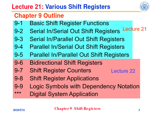
Lecture 15: Latches and Flip-Flops Basics Chapter 7 Outline 7-1 7-2 **** 7-3 7-4 Latches Lecture 15 Edge-Triggered Flip-Flops Lecture 16 Flip-Flop Evolution Flip-Flop Operating Characteristics Flip-Flop Applications
Chapter 7 Latches, Flip-Flops, and Timers
11
Lecture 15: Latches and Flip-Flops Basics
Active-LOW S-R Latch Example If the S and R waveforms shown below are applied to the inputs of the active-LOW latch, determine the waveform on the Q output. Assume Q is initially “0”.
2012-3-28
我们如何用SR锁存器来解决 我们如何用 锁存器来解决 这个问题呢? 这个问题呢?
Chapter 7 Latches, Flip-Flops, and Timers
13
Chapter 7 Latches, Flip-Flops, and Timers
2
Lecture 15: Latches and Flip-Flops Basics
Inverter Bistable Circuit Look at the following circuit:
U4
Lecture 15: Latches and Flip-Flops Basics Chapter 7 Outline 7-1 7-2 **** 7-3 7-4 Latches Lecture 15 Edge-Triggered Flip-Flops Lecture 16 Flip-Flop Evolution Flip-Flop Operating Characteristics Flip-Flop Applications
Chapter 7 Latches, Flip-Flops, and Timers
11
Lecture 15: Latches and Flip-Flops Basics
Active-LOW S-R Latch Example If the S and R waveforms shown below are applied to the inputs of the active-LOW latch, determine the waveform on the Q output. Assume Q is initially “0”.
2012-3-28
我们如何用SR锁存器来解决 我们如何用 锁存器来解决 这个问题呢? 这个问题呢?
Chapter 7 Latches, Flip-Flops, and Timers
13
数字电路英文版第四单元PPT课件

A(B+C )=AB+AC
第19页/共135页
9.
B
B+C
A
B C
X
A
A
C
AB X
AC
X = A( B + C ) X = A B + A C
第20页/共135页
10.
Rules of Boolean Algebra
1. A + 0 = A 7. A * A = A
2. A + 1 = 1 8. A * A = 0
• “Don’t care” A combination of input literals that cannot occur and can be used as a 1 or a 0 on a Karnaugh map.
第5页/共135页
• Literal A variable or the complement of a variable. • Product-of-sums (POS) A form of Boolean expression that is
第3页/共135页
• Commutative law In addition (ORing) and multiplication (ANDing) of two variables, the order in which the variables are ORed orANDed makes no diffence.
A+B=B+A
A
A+B
B
B
A
第15页/共135页
B+A
5.
Logical Multiplication
数字电子技术(课件)lec22
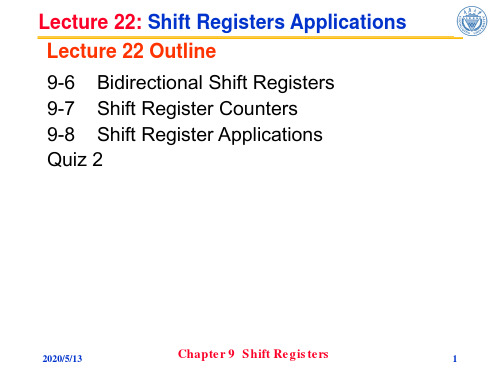
Lecture 22: Shift Registers Applications Lecture 22 Outline 9-6 Bidirectional Shift Registers 9-7 Shift Register Counters 9-8 Shift Register Applications Quiz 2
Sample Timing Diagram for a 74HC194 Shift Register
2013-7-28
Chapter 9 Shift Registers
9
Lecture 22: Shift Registers Applications
Shift Register Counters A shift register counter is basically a shift register with the serial output connected back to the serial input to produce special sequences. The Johnson Counter (扭环计数器) In a Johnson counter, the complement of the output of the last flip-flop is connected back to the D input of the first flip-flop. See circuits on the next page. In general, a Johnson counter will produce a modulus of 2n sequence, where n is the number of stages in the counter. The produced sequences for the 4 and 5-stage Johnson counter are shown on next page. You will notice that the counter will „fill up‟ with 1s from left to right, and then it will „fill up‟ with 0s again.
数字电子技术(课件)lec21
Rising edge shifting
Inhibit shifting Asynchronous loading
Loaded data
No shifting in this interval
2012-3-28
Chapter 9 Shift Registers
15
Lecture 21: Various Shift Registers
A Serial In/Parallel Out Shift Register The output for each stage is available simultaneously.
In order to use the above circuit in real world, we need to use a parallel read out signal to take the data out. Detailed circuit is shown by the side.
Therefore, when this input is LOW, The register is loaded with parallel data asynchronously. The clock can be inhibited any time with a HIGH on this input. Rising edge shifting
2012-3-28
Chapter 9 Shift Registers
3
Lecture 21: Various Shift Registers
Basic Types of Data Movement in Shift Registers
2012-3-28
Chapter 9 Shift Registers
《电子技术数字基础 Digital Fundamentals》双语课件PPT-第08章 Counters (1)
11
8-2-1 1 Analysis of the Sequential Logic – State Sequence Table (状态转换表)
Q1Q0 00 Q1Q0 01
Q1Q0 10
n 1
2. Q0
Q0 (CLK )
QCP Q0Q1 Q0Q10 (CLK ) Q1 Q 1
27
8-1-1 Analysis of Asynchronous Sequential Logic State Diagram
State Sequence Table
A asynchronous decade counter (异步十进制加法计数器)
28
8-1-2 Some Useful Concepts
0
1
n 1
Q1Q0 11
0
0
0able
2
3
1
1
0
1
4
0
0
12
8-2-1 Analysis of the Sequential Logic – State Diagram (状态转换图)
State Sequence Table
CP
0 1 2 3 4
State Diagram
2. 将驱动方程代入触发器的特性方程,得到状态方程组;
8
8-2-1 Analysis of the Sequential Logic Procedure
3. Write down the output expression;
3. 写出输出方程;
4. Assume the present state, and analyze the next state, and draw its state diagram (状态转换图) /state sequence table(状态转换表)or its timing diagram (时序图)
数字电子技术,英文版,chapter02

The Weighting Structure of Binary Numbers A binary number is a weighted number(加权数). number(加权数). The right-most bit is the LSB(最低有效位) in a rightLSB(最低有效位) binary whole number and has a weight of 20=1. The weights increase from right to left by a power of two for each bit. The left-most bit is the MSB(最 leftMSB(最 高有效位). 高有效位). Fractional numbers(小数) can also be represented numbers(小数) in binary by placing bits to the right of the binary point. point. The left-most bit is the MSB in a binary leftfractional number and has a weight of 2-1=0.5. The fractional weights decreases from left to right by a negative power of two for each bit. The weight structure of a binary number is
– Not really. – Probably the fact that we have 10 fingers influenced this.
Will a base other than 10 work?
数字电子技术基础英文版课件
Slide 16
Logic Levels
Binary values are also represented by voltage levels
They can also be called LOW and HIGH, where LOW = 0 and HIGH = 1 In positive logic rules:
Slide 14
1-2 Binary Digits, Logic Levels, and Digital Waveforms 二进制数,逻辑电平和数字波形
Slide 15
Binary Digits
• The conventional numbering system uses ten digits: 0,1,2,3,4,5,6,7,8, and 9. • The binary numbering system uses just two digits: 0 and 1. • Each of the two digits is called bit, which is a contraction of the words binary digit. • Groups of bits (combinations of 1s and 0s)is called code.
1 f T
Slide 21
An important characteristic of a digital waveform is its duty cycle. The duty cycle(占空比) of a binary waveform is defined as:
tw Duty cycle 100% T
Slide 17
Slide 18
- 1、下载文档前请自行甄别文档内容的完整性,平台不提供额外的编辑、内容补充、找答案等附加服务。
- 2、"仅部分预览"的文档,不可在线预览部分如存在完整性等问题,可反馈申请退款(可完整预览的文档不适用该条件!)。
- 3、如文档侵犯您的权益,请联系客服反馈,我们会尽快为您处理(人工客服工作时间:9:00-18:30)。
Slide 14
1-2 Binary Digits, Logic Levels, and Digital Waveforms 二进制数,逻辑电平和数字波形
Slide 15
Байду номын сангаас
Binary Digits
• The conventional numbering system uses ten digits: 0,1,2,3,4,5,6,7,8, and 9. • The binary numbering system uses just two digits: 0 and 1. • Each of the two digits is called bit, which is a contraction of the words binary digit. • Groups of bits (combinations of 1s and 0s)is called code.
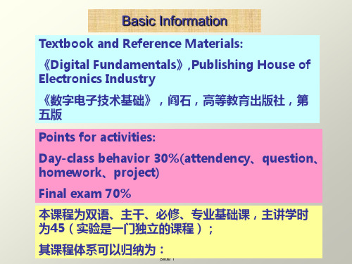
Basic Information
Textbook and Reference Materials: 《Digital Fundamentals》,Publishing House of Electronics Industry 《数字电子技术基础》,阎石,高等教育出版社,第 五版 Points for activities: Day-class behavior 30%(attendency、question、 homework、project) Final exam 70% 本课程为双语、主干、必修、专业基础课,主讲学时 为45(实验是一门独立的课程); 其课程体系可以归纳为:
Slide 4
模拟电路研究的问题
基本电路元件:
•晶体三极管 •场效应管 •集成运算放大器
基本模拟电路:
• 信号放大及运算 (信号放大、功率放大)
• 信号处理(采样保持、电压比较、有源滤波)
• 信号发生(正弦波发生器、三角波发生器、…)
Slide 5
数字电路研究的问题
基本电路元件 基本数字电路
• 组合逻辑电路 • 时序电路(寄存器、计数器、脉冲发生器、 脉冲整形电路) • A/D转换器、D/A转换器 • 逻辑门电路 • 触发器
Slide 16
Logic Levels
Binary values are also represented by voltage levels
They can also be called LOW and HIGH, where LOW = 0 and HIGH = 1 In positive logic rules:
Slide 22
The Digital Advantages in Electronics Application 1.Digital data can be processed and transmitted more efficiently and reliably than analog data.
(Noise does not affect digital data as much as it does analog signals) 2.Digital data has a great advantage when storage is necessary. 网上参考资料: /b/8866165.html
Slide 6
TTL NAND Gate
+5V
R1
T1 A B C
R2
T3
R4 T4 Y T5
T2
多发射极 三极管
R3
R5
输入级
中间级
Slide 7
输出级
• S-R latch
Slide 8
Digital Fundamentals
CHAPTER 1 Digital Concepts
Slide 9
Slide 20
Digital Waveforms(ideal pulse:for most digital work we can assume ideal pulse)
• tw = pulse width • T = period of the waveform • f = frequency of the waveform; reciprocal of the period.
1 f T
Slide 21
An important characteristic of a digital waveform is its duty cycle. The duty cycle(占空比) of a binary waveform is defined as:
tw Duty cycle 100% T
Slide 3
模拟电路与数字电路比较
1.电路的特点
在模拟电路中,晶体管一般工作在线性放大区; 在数字电路中,三极管工作在开关状态,即工 作在饱和区和截止区。
2.研究的内容
模拟电路主要研究:输入、输出信号间的大小、 相位、失真等方面的关系。主要采用电路分 析方法,动态性能用微变等效电路分析。 数字电路主要研究:电路输出、输入间的逻辑关系。 主要的工具是逻辑代数,电路的功能用真值表、 逻辑表达式及波形图表示。
Slide 11
Digital and Analog Quantities
Types of electronic devices or instruments: • Analog • Digital • Combination analog and digital
Slide 12
Slide 13
Slide 1
Course Description
Slide 2
逻辑代数基础(第4章) 组合逻辑电路
(以第3章逻辑门 作为基本的逻辑 单元电路,在第5、 6章进行具体介绍)
时序逻辑电路
(以第7章触发器作 为基本的逻辑单元 电路,在第8、9介 绍不同的时序逻辑 电路)
半导体存储器(第10章) A/D转换(第11章)
1-1 Digital and Analog Quantities (数字量和模拟量)
Slide 10
Digital and Analog Quantities
Analog quantities have continuous values
Digital quantities have discrete sets of values
Slide 17
Slide 18
Logic Levels
CMOS
HIGH: 2-3.3V
LOW: 0-0.8V
Slide 19
Digital Waveforms (made up of a series of pulses)
Major parts of a digital pulse (nonideal pulse: In practice transitions never occur instantaneously) • Base line(基线) • Amplitude(幅值) • Rise time (tr)(上升时间) • Pulse width (tw) (脉冲宽度) • Fall time (tf) (下降时间)
1-2 Binary Digits, Logic Levels, and Digital Waveforms 二进制数,逻辑电平和数字波形
Slide 15
Байду номын сангаас
Binary Digits
• The conventional numbering system uses ten digits: 0,1,2,3,4,5,6,7,8, and 9. • The binary numbering system uses just two digits: 0 and 1. • Each of the two digits is called bit, which is a contraction of the words binary digit. • Groups of bits (combinations of 1s and 0s)is called code.
Basic Information
Textbook and Reference Materials: 《Digital Fundamentals》,Publishing House of Electronics Industry 《数字电子技术基础》,阎石,高等教育出版社,第 五版 Points for activities: Day-class behavior 30%(attendency、question、 homework、project) Final exam 70% 本课程为双语、主干、必修、专业基础课,主讲学时 为45(实验是一门独立的课程); 其课程体系可以归纳为:
Slide 4
模拟电路研究的问题
基本电路元件:
•晶体三极管 •场效应管 •集成运算放大器
基本模拟电路:
• 信号放大及运算 (信号放大、功率放大)
• 信号处理(采样保持、电压比较、有源滤波)
• 信号发生(正弦波发生器、三角波发生器、…)
Slide 5
数字电路研究的问题
基本电路元件 基本数字电路
• 组合逻辑电路 • 时序电路(寄存器、计数器、脉冲发生器、 脉冲整形电路) • A/D转换器、D/A转换器 • 逻辑门电路 • 触发器
Slide 16
Logic Levels
Binary values are also represented by voltage levels
They can also be called LOW and HIGH, where LOW = 0 and HIGH = 1 In positive logic rules:
Slide 22
The Digital Advantages in Electronics Application 1.Digital data can be processed and transmitted more efficiently and reliably than analog data.
(Noise does not affect digital data as much as it does analog signals) 2.Digital data has a great advantage when storage is necessary. 网上参考资料: /b/8866165.html
Slide 6
TTL NAND Gate
+5V
R1
T1 A B C
R2
T3
R4 T4 Y T5
T2
多发射极 三极管
R3
R5
输入级
中间级
Slide 7
输出级
• S-R latch
Slide 8
Digital Fundamentals
CHAPTER 1 Digital Concepts
Slide 9
Slide 20
Digital Waveforms(ideal pulse:for most digital work we can assume ideal pulse)
• tw = pulse width • T = period of the waveform • f = frequency of the waveform; reciprocal of the period.
1 f T
Slide 21
An important characteristic of a digital waveform is its duty cycle. The duty cycle(占空比) of a binary waveform is defined as:
tw Duty cycle 100% T
Slide 3
模拟电路与数字电路比较
1.电路的特点
在模拟电路中,晶体管一般工作在线性放大区; 在数字电路中,三极管工作在开关状态,即工 作在饱和区和截止区。
2.研究的内容
模拟电路主要研究:输入、输出信号间的大小、 相位、失真等方面的关系。主要采用电路分 析方法,动态性能用微变等效电路分析。 数字电路主要研究:电路输出、输入间的逻辑关系。 主要的工具是逻辑代数,电路的功能用真值表、 逻辑表达式及波形图表示。
Slide 11
Digital and Analog Quantities
Types of electronic devices or instruments: • Analog • Digital • Combination analog and digital
Slide 12
Slide 13
Slide 1
Course Description
Slide 2
逻辑代数基础(第4章) 组合逻辑电路
(以第3章逻辑门 作为基本的逻辑 单元电路,在第5、 6章进行具体介绍)
时序逻辑电路
(以第7章触发器作 为基本的逻辑单元 电路,在第8、9介 绍不同的时序逻辑 电路)
半导体存储器(第10章) A/D转换(第11章)
1-1 Digital and Analog Quantities (数字量和模拟量)
Slide 10
Digital and Analog Quantities
Analog quantities have continuous values
Digital quantities have discrete sets of values
Slide 17
Slide 18
Logic Levels
CMOS
HIGH: 2-3.3V
LOW: 0-0.8V
Slide 19
Digital Waveforms (made up of a series of pulses)
Major parts of a digital pulse (nonideal pulse: In practice transitions never occur instantaneously) • Base line(基线) • Amplitude(幅值) • Rise time (tr)(上升时间) • Pulse width (tw) (脉冲宽度) • Fall time (tf) (下降时间)