ST58812移动电源方案
ST L9945八路12V和24V系统全配置高-低边MOSFET预驱动解决方案

ST公司的L9945是八路MOSFET预驱动器,可配置成用于低边,高边,峰值和保持以及H桥负载的控制,设计用于12V(客车)和24V(商用车)电池系统.所有输出是PWM控制的,其中6个输出能安全驱动相关载荷,一个能激励需要专用使能引脚(EN6)的相关载荷.L9945提供控制两个单独H桥的功能,还能驱动多达两个需要”峰值保持”控制的负载.每个输出提供全部的诊断信息如对电池短路,对地短路和负载开路.而每个输出状态能不断通过专用SPI寄存器进行监测.器件满足AEC-Q100规范,3.3V和5V逻辑兼容I/O,工作电池电压3.8V到36V,工作的VDD电压4.5V-5.5V,L9945中的10位ADC通过SPI对电池和芯片温度进行测量.主要用在汽车电子.本文介绍了L9945主要特性,框图以及评估板EVAL-L9945及其应用框图,配置框图,电路图,材料清单和PCB设计图.The L9945 is an 8-channel MOSFET pre-driver configurable for low-side, high-side, peak and hold and H-Bridge load control. It is designed to comply with the requirements of 12 V (passenger vehicle) and 24 V(commercial vehicle) battery systems.All outputs can be PWM controlled. Six outputs are capable of driving safety relevant loads. One output can be dedicated to the actuation ofsafety relevant loads requiring a dedicated enable pin (EN6).The device offers the possibility of controlling two independent H-Bridges.The device can also drive up to two loads requiring "peak & hold"control strategy.The driver outputs are protected against short circuit condition.The device protects the external MOS in case of an overcurrent event.Each output provides full diagnostic information such as short tobattery, short to ground and open-load. Each output status can beconstantly monitored through dedicated SPI registers.The voltage slew rate of the external transistors 1-8 is controlled during turn ON and turn OFF in order to improve EMI behavior. A double,redundant, external disable source is available through DIS and NDIS pins in order to improve safety. The device is configurable via SPI through a 32-bit protocol.L9945主要特性:AEC-Q100 qualified12 V and 24 V battery systems compliance3.3 V and 5 V logic compatible I/O8-channel configurable MOSFET pre-driverHigh-side (N-channel and P-channel MOS)Low-side (N-channel MOS)H-bridge (up to 2 H-bridge)Peak & Hold (2 loads)ST L9945八路12V和24V系统全配置高-低边MOSFET预驱动解决方案Operating battery supply voltage 3.8 V to 36 VOperating VDD supply voltage 4.5 V to 5.5 VAll device pins, except the ground pins, withstand at least 40 V Programmable gate charge/discharge currents for improving EMI behavior Individual diagnosis for:Short circuit to batteryOpen loadShort circuit to groundHighly flexible overcurrent sensing implementationPossibility of monitoring external MOS drain to source voltage Possibility of monitoring voltage on external shunt resistor64 programmable overcurrent thresholds independent for each channel Ultra-fast output shutdown in case of overcurrentCurrent limitation for H-Bridge configuration32-bit SPI protocol available for configuration and diagnostics Failures latched even if they occur during diagnostics reading Daisy chain operationSDO protected against overvoltageSafety featuresFast switch off redundant output disable through two external pins Built InSelf Test (BIST) for logic operationHardware Self Check (HWSC) for VDD5 overvoltage comparator Configurable Communication Check (CC) watchdog timer available Disable feedback through bi-directional pinHighly redundant output monitoring through dedicated SPI registers 10-bit ADC for battery and die temperature measurements available through SPI VDD5 monitoring for over/under voltageVPS (battery) monitoring for under voltage图1:L9945框图(1)图2:L9945框图(2)。
移动电源各有优缺点 测评

移动电源:各有优缺点性价比是王道川北在线-川北城市生活网 2013-10-17 19:35 来源:赛迪网川北在线核心提示:天猫4款热销移动电源横评随着电子产品的迅猛发展,移动电源经历了普通电源、智能移动电源后,迈进超智能移动电源发展阶段(资料来源于百科)。
而由于巨大的市场份额,移动电源成为电子配件行业颇受重视的门类,也成为电子消费者的必备品。
不过许多消费者对移动电源并天猫4款热销移动电源横评随着电子产品的迅猛发展,移动电源经历了普通电源、智能移动电源后,迈进超智能移动电源发展阶段(资料来源于百科)。
而由于巨大的市场份额,移动电源成为电子配件行业颇受重视的门类,也成为电子消费者的必备品。
不过许多消费者对移动电源并不了解,导致往往购买到劣质产品。
为帮助消费者更好地挑选移动电源,我们针对天猫里移动电源的销量占比以及搜索热度,挑选了4个品牌,包括:品能PN-913、罗马仕sense4、力杰 V8、飞毛腿TP BM788移动电源,从电源重量、尺寸、价格、性能等维度进行横向对比,为大家分析与讲解一下目前主流移动电源产品。
从这4款单品月销售来看,总销量已经达到了20多万,占据了整个移动电源销量约40%的份额;所以这里的4款产品就已经很好地代表着整个移动电源的发展趋势。
(4款淘宝热销移动电源)如上图所示,其中,品能PN-913单品月销量就已经达到8.2W;排名第二罗马仕sense 4销量5.3W;排名第三品能PN-913月销量5.2W;排名第四飞毛腿TP:2.6W;以评论数量估算产品销售额。
品能PN-913单品销售额约为 19W*99元=1881万元;罗马仕ROMOSS sense 4评论数量14W,14W*79.9元=1118.6万元。
这就是为何越来越多的厂商仍狂推出新款移动电源产品的原因!!!下面我们就将对这4款热销宝贝进行较为详细的评测。
但因为内容较多详细,文章篇幅也不短。
我们将评测核心参数汇总提前。
大家可以通过以下表格很清楚地看到4款电源的对比。
移动电源五合一方案
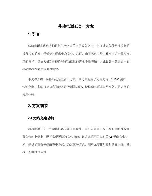
移动电源五合一方案1. 引言移动电源是现代人们日常生活必备的电子设备之一,它可以为各种便携式电子设备(如手机、平板等)提供电力支持。
然而,由于现有市场上移动电源产品多样,功能各异,以及人们对便捷性和多功能性的需求不断增加,因此设计一款五合一的移动电源方案成为迫切需要。
本文将介绍一种移动电源五合一方案,该方案融合了无线充电、USB C接口、快速充电、多输出接口和智能芯片控制等功能,使移动电源具备更高效、更方便的使用体验。
2. 方案细节2.1 无线充电功能移动电源五合一方案将具备无线充电功能,用户只需将支持无线充电的设备放置在移动电源上,即可实现无线的充电功能。
该方案采用了先进的Qi无线充电技术,提供了高效便捷的充电方式。
通过这种方式,用户无需使用额外的充电线,减少了充电时的麻烦。
2.2 USB C接口为了满足现代设备的需求,该移动电源方案配备了USB C接口。
USB C接口具备更高的传输速度和更大的功率输出能力,可以实现快速充电和高效传输数据。
用户可以使用USB C线充电,也可以通过USB C接口连接其他设备进行数据传输。
2.3 快速充电为了提升用户的充电效率,移动电源五合一方案支持快速充电功能。
方案中采用了智能识别技术,能够根据设备充电需求自动调节输出功率,实现更快的充电速度。
同时,方案还具备快速充电保护功能,可以避免过度充电和过热问题,保护设备的使用安全。
2.4 多输出接口该移动电源方案提供了多种输出接口,以满足用户不同设备充电需求。
除了USB C接口,方案还配备了USB A接口和Micro USB接口,用户可以根据实际需求选择合适的接口进行充电。
这些输出接口可以同时支持多个设备的充电,提高了移动电源的实用性。
2.5 智能芯片控制移动电源五合一方案采用了智能芯片控制技术,实现了对电源的智能管理。
该方案可以实时监测电源的电量,显示剩余电量,并提供智能充电保护功能。
当电量过低或过高时,方案会自动停止充电,避免对设备和电池的损害。
IT8512+ 用户手册

直流可编程电子负载IT8500+系列用户手册型号:IT8511+/IT8511A+/IT8511B+/IT8512+/IT8512A+/IT8512B+/IT8512C+/IT8512H+/IT8513C+/IT8514C+/IT8514B+/IT8516C+版本号:4.1声明© Itech Electronics, Co., Ltd. 2014根据国际版权法,未经Itech Electronics, Co., Ltd. 事先允许和书面同意,不得以任何形式(包括电子存储和检索或翻译为其他国家或地区语言)复制本手册中的任何内容。
手册部件号IT8500+-402008版本第4版,2015 年05月18日发布Itech Electronics, Co., Ltd.商标声明Pentium是Intel Corporation在美国的注册商标。
Microsoft、Visual Studio、Windows 和MS Windows是Microsoft Corporation 在美国和/或其他国家/地区的商标。
担保本文档中包含的材料“按现状”提供,在将来版本中如有更改,恕不另行通知。
此外,在适用法律允许的最大范围内,ITECH 不承诺与本手册及其包含的任何信息相关的任何明示或暗含的保证,包括但不限于对适销和适用于某种特定用途的暗含保证。
ITECH对提供、使用或应用本文档及其包含的任何信息所引起的错误或偶发或间接损失概不负责。
如ITECH与用户之间存在其他书面协议含有与本文档材料中所包含条款冲突的保证条款,以其他书面协议中的条款为准。
技术许可本文档中描述的硬件和/或软件仅在得到许可的情况下提供并且只能根据许可进行使用或复制。
限制性权限声明美国政府限制性权限。
授权美国政府使用的软件和技术数据权限仅包括那些定制提供给最终用户的权限。
ITECH 在软件和技术数据中提供本定制商业许可时遵循FAR 12.211(技术数据)和12.212(计算机软件)以及用于国防的DFARS252.227-7015(技术数据-商业制品)和DFARS 227.7202-3(商业计算机软件或计算机软件文档中的权限)。
LC8812B-5050RGBW规格书
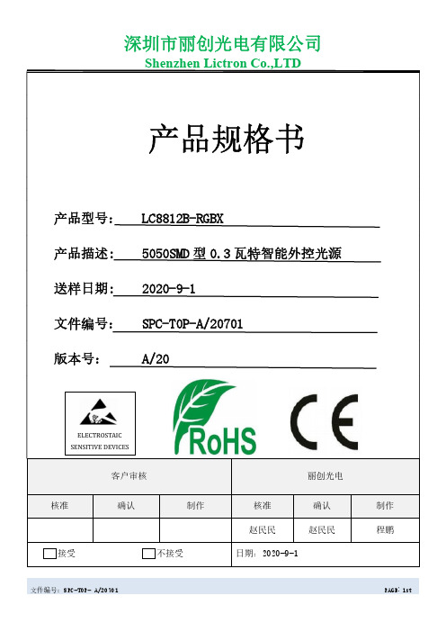
ELECTROSTAICSENSITIVE DEVICES制作核准接受不接受6.RGBW芯片特性参数Ta=25℃:TOHTOLT1HT1LTreset0码1码Reset 码DIN DO PIX1DINDOPIX2D1D2D3D4DINDOPIX3注:其中复位码>=80us数据刷新周期表1复位码D1D2D3D4注:高位先发,按照GRBW 的顺序发送数据(G7→G6→ 005V1045V104U1U25V104U3RR辐射图特性曲线17.包装规格:载带规格(单位:mm)卷轴尺寸:防潮带包装:标签描述:PRODUCT NO:产品型号QUANTITY:包装数量LOT NO:指令单号CCT:色温BIN:色区代码Ra:显数指数DATE:生产日期注明:SMD5050系列包装标准1000PCS/包,特别要求除外。
标签示图贴标签位贴标签位注:标注公差为±0.1mm,单位:mmPRODUCT NO:QUANTITY:PCSLOT NO:DATE:Lead freePRODUCT NO:产品型号QUANTITY:包装数量LOT NO:指令单号DATE:生产日期1.6.已完成装配的灯珠元件进行防潮管控对需要进行二次SMT工艺或高温的产品,在完成一次焊接后将会进行二次焊接前,亦应做好必要的防潮处理,暴露在(≦30℃/60%RH)条件下,最长不能超过2H,若二次高温生产相隔时间较长,则一次焊接后的材料必需进行必要的除湿工作(在70℃±5℃的烤箱中烘烤不少于12小时),然后抽真空密封保存,或者先将产品储存在干燥箱恒温恒湿箱内,二次高温生产前,再做进行除湿工作(在70℃±5℃的烤箱中烘烤不少于12小时),以确保产品在过高温工艺前不受潮,低湿烘烤条件:70℃±5℃烘烤不小于12小时高温烘烤条件:130°C±5°C烘烤5小时,回流焊正常作业累计不超过3次,对挤出工艺或者高温防护处理的产品,建议产品做防护工艺前,做好必要的除湿工作,在130℃±5℃的烤箱中烘烤5小时,以剔除产品在检测,老化,运输过程中暴露在空气中吸收的湿气,以避免产品在做防护处理后,包在材料表面的湿气会慢慢侵入材料,造成产品失效,1.7.回流焊焊接经丽创光电采用下面所列参数检测证明,表面贴装型LED符合JEDEC J-STD-020C标准。
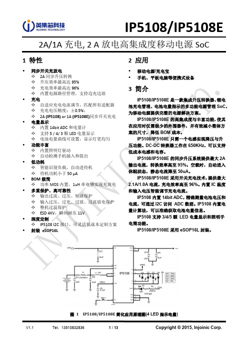
IP5108_brief
主要特点 LED 灯数 1,2 3,4 3,4,5 3,4,5 3,4,5 3,4,5 3,4,5 3,4,5 3,4,5 照明灯 √ √ √ √ √ √ √ √ 按键 √ √ √ √ √ √ √ √
封装
手机充电 电流识别
充电 1.0A 1.2A 1.5A 1.0A 2.1A 1.2A 3.0A 3.0A图 1
V1.1
IP5108/IP5108E 简化应用原理图(4 LED 指示电量)
1 / 13
Tel:13510832836
Copyright © 2015, Injoinic Corp.
IP5108/IP5108E
4 引脚定义
ESOP16L 1 2 3 4 5 6 7 8 CSIN GND LX LX VOUT VOUT VIN LIGHT 17
无 100% 80%
无 无 100%
IP5108/IP5108E 自动检测手机插入, 即刻从待机态唤醒,打开升压 5V 给手机充电,省去 按键操作, 支持无按键模具方案。 如果不需要手机插入自动开机的功能, 需要在订购的时候说明, 并且在 VOUT 上加 1K 的下拉电阻到 GND。
充电
IP5108/IP5108E 拥有一个同步开关结构的恒流、恒压锂电池充电器。当电池电压小于 3V 时,采用 100mA涓流充电;当电池电压大于3V,进入恒流充电;当电池电压大于4.2V, 进入恒压充电。充电完成 后,若电池电压低于4.1V后,重新开启电池充电。 IP5108 采用开关充电技术,开关频率 1.6MHz,最大充电电流 2.1A,充电效率最高到 96%,能缩短 3/4 的充电时间。IP5108E 充电电流为 1.0A。 自适应电源路径管理,优先给外部负载供电,支持边充边放。 IP5108/IP5108E 会自动调节充电电流大小,来适应不同负载能力的适配器,确保不拉挂适配器。
MAX8510 MAX8511 MAX8512 极低噪声、低掉电的线性调压器说明说明书
General DescriptionThe MAX8510/MAX8511/MAX8512 ultra-low-noise, low-dropout (LDO) linear regulators are designed to deliver up to 120mA continuous output current. These regulators achieve a low 120mV dropout for 120mA load current. The MAX8510 uses an advanced architecture to achieve ultra-low output voltage noise of 11μV RMS and PSRR of 54dB at 100kHz.The MAX8511 does not require a bypass capacitor, hence achieving the smallest PC board area. The MAX8512’s output voltage can be adjusted with an external divider.The MAX8510/MAX8511 are preset to a variety of voltag-es in the 1.5V to 4.5V range. Designed with a P-channel MOSFET series pass transistor, the MAX8510/MAX8511/MAX8512 maintain very low ground current (40μA).The regulators are designed and optimized to work with low-value, low-cost ceramic capacitors. The MAX8510 requires only 1μF (typ) of output capacitance for stability with any load. When disabled, current consumption drops to below 1μA.Package options include a 5-pin SC70 and a tiny 2mm x 2mm x 0.8mm TDFN package.Applications●Cellular and Cordless Phones ●PDA and Palmtop Computers ●Base Stations●Bluetooth Portable Radios and Accessories ●Wireless LANs ●Digital Cameras ●Personal Stereos●Portable and Battery-Powered EquipmentFeatures●Space-Saving SC70 and TDFN (2mm x 2mm) Packages ●11μV RMS Output Noise at 100Hz to 100kHzBandwidth (MAX8510)●78dB PSRR at 1kHz (MAX8510) ●120mV Dropout at 120mA Load●Stable with 1μF Ceramic Capacitor for Any Load ●Guaranteed 120mA Output●Only Need Input and Output Capacitors (MAX8511) ●Output Voltages: 1.5V, 1.8V, 2.5V, 2.6V, 2.7V, 2.8V,2.85V, 3V,3.3V,4.5V (MAX8510/MAX8511) and Adjustable (MAX8512) ●Low 40μA Ground Current ●Excellent Load/Line Transient●Overcurrent and Thermal Protection19-2732; Rev 5; 5/19Output Voltage Selector Guide appears at end of data sheet.Ordering Information continued at end of data sheet.*xy is the output voltage code (see Output Voltage Selector Guide). Other versions between 1.5V and 4.5V are available in 100mV increments. Contact factory for other versions.+Denotes a lead(Pb)-free/RoHS-compliant package.T = Tape and reel.PART*TEMP RANGE PIN-PACKAGEMAX8510EXKxy+T -40°C to +85°C 5 SC70MAX8510/MAX8511/MAX8512Ultra-Low-Noise, High PSRR,Low-Dropout, 120mA Linear RegulatorsOrdering InformationClick here for production status of specific part numbers.IN to GND ................................................................-0.3V to +7V Output Short-Circuit Duration ...........................................Infinite OUT, SHDN to GND .....................................-0.3V to (IN + 0.3V)FB, BP , N.C. to GND ................................-0.3V to (OUT + 0.3V)Continuous Power Dissipation (T A = +70°C)5-Pin SC70 (derate 3.1mW/°C above +70°C) .............0.247W 8-Pin TDFN (derate 11.9mW/°C above = 70°C) .........0.953W Operating Temperature Range ...........................-40°C to +85°CMilitary Operating Temperature Range .............-55°C to +110°C Junction Temperature ......................................................+150°C Storage Temperature Range ............................-65°C to +150°C Lead Temperature (soldering, 10s) .................................+300°C Soldering Temperature (reflow) .......................................+260°C Lead (Pb)-free packages .................................................+260°C Packages containing lead (Pb) .......................................+240°C(Note 1)SC70Junction-to-Ambient Thermal Resistance (θJA ) ........324°C/W Junction-to-Case Thermal Resistance (θJC ) .............115°C/WTDFNJunction-to-Ambient Thermal Resistance (θJA ) .......83.9°C/W Junction-to-Case Thermal Resistance (θJC ) ...............37°C/W(V IN = V OUT + 0.5V, T A = -40°C to +85°C, unless otherwise noted. C IN = 1μF, C OUT = 1μF, C BP = 10nF. Typical values are at +25°C; the MAX8512 is tested with 2.45V output, unless otherwise noted.) (Note 2)PARAMETER SYMBOL CONDITIONSMIN TYPMAX UNITS Input Voltage Range V IN26VOutput Voltage Accuracy I OUT = 1mA, T A = +25°C-1+1%I OUT = 100µA to 80mA, T A = +25°C -2+2I OUT = 100µA to 80mA-3+3Maximum Output Current I OUT 120mA Current LimitI LIMV OUT = 90% of nominal value 130200300mA Dropout Voltage (Note 3)V OUT ≥ 3V, I OUT = 80mA 80170mVV OUT ≥ 3V, I OUT = 120mA1202.5V ≤ V OUT < 3V, I OUT = 80mA 902002.5V ≤ V OUT < 3V, I OUT = 120mA 1352V ≤ V OUT < 2.5V, I OUT = 80mA 1202502V ≤ V OUT < 2.5V, I OUT = 120mA180Ground Current I Q I OUT = 0.05mA4090µA V IN = V OUT (nom) - 0.1V, I OUT = 0mA 220500Line Regulation V LNR V IN = (V OUT + 0.5V) to 6V, I OUT = 0.1mA 0.001%/V Load RegulationV LDR I OUT = 1mA to 80mA 0.003%/mA Shutdown Supply CurrentI SHDNV SHDN = 0VT A = +25°C 0.0031µAT A = +85°C 0.05Ripple RejectionPSRRf = 1kHz, I OUT = 10mAMAX851078dBMAX8511/MAX851272f = 10kHz, I OUT = 10mA MAX851075MAX8511/MAX851265f = 100kHz, I OUT = 10mAMAX851054MAX8511/ MAX851246MAX8512Low-Dropout, 120mA Linear RegulatorsAbsolute Maximum RatingsStresses beyond those listed under “Absolute Maximum Ratings” may cause permanent damage to the device. These are stress ratings only, and functional operation of the device at these or any other conditions beyond those indicated in the operational sections of the specifications is not implied. Exposure to absolute maximum rating conditions for extended periods may affect device reliability.Electrical CharacteristicsPackage Thermal Characteristics Note 1: Package thermal resistances were obtained using the method described in JEDEC specification JESD51-7, using a four-layerboard. For detailed information on package thermal considerations, refer to /thermal-tutorial .(V IN = V OUT + 0.5V, T A = -40°C to +85°C, unless otherwise noted. C IN = 1μF, C OUT = 1μF, C BP = 10nF. Typical values are at +25°C; the MAX8512 is tested with 2.45V output, unless otherwise noted.) (Note 2)Note 2: Limits are 100% tested at +25°C. Limits over operating temperature range are guaranteed by design.Note 3: Dropout is defined as V IN - V OUT when V OUT is 100mV below the value of V OUT for V IN = V OUT + 0.5V.Note 4: Time needed for V OUT to reach 90% of final value.(V IN = V OUT + 0.5V, C IN = 1μF, C OUT = 1μF, C BP = 10nF, T A = +25°C, unless otherwise noted.)PARAMETER SYMBOLCONDITIONSMINTYP MAXUNITSOutput Noise Voltage (RMS)f = 100Hz to 100kHz, I LOAD = 10mA MAX851011µVMAX8511/MAX8512230f = 100Hz to 100kHz, I LOAD = 80mA MAX851013MAX8511/MAX8512230Shutdown Exit Delay R LOAD = 50Ω (Note 4)300µs SHDN Logic Low Level V IN = 2V to 6V 0.4V SHDN Logic High Level V IN = 2V to 6V 1.5V SHDN Input Bias Current V IN = 6V, V SHDN = 0V or 6VT A = +25°C µA T A = +85°C 0.01FB Input Bias Current (MAX8512)V IN = 6V,V FB = 1.3VT A = +25°C 0.0060.1µA T A = +85°C0.01Thermal Shutdown 160°C Thermal-Shutdown Hysteresis10°C MAX8510OUTPUT VOLTAGE ACCURACYvs. LOAD CURRENTM A X 8510 t o c 02LOAD CURRENT (mA)% D E V I A T I O N (%)10080604020-0.4-0.200.20.40.6-0.60120MAX8510OUTPUT VOLTAGE ACCURACYvs. TEMPERATURETEMPERATURE (°C)% D E V I A T I O N (%)603510-15-0.8-0.6-0.4-0.200.20.40.60.81.0-1.0-4085MAX8510OUTPUT VOLTAGE vs. INPUT VOLTAGEINPUT VOLTAGE (V)O U T P U T V O L T A G E (V )543210.51.01.52.02.53.00.06MAX8512Low-Dropout, 120mA Linear RegulatorsElectrical Characteristics (continued)Typical Operating Characteristics(V IN = V OUT + 0.5V, C IN = 1μF, C OUT = 1μF, C BP = 10nF, T A = +25°C, unless otherwise noted.)MAX8510DROPOUT VOLTAGE vs. OUTPUT VOLTAGEOUTPUT (V)D R O P O U T V O L T A G E (m V )3.02.82.62.42.2501001502002502.03.2MAX8510GROUND PIN CURRENT vs. TEMPERATUREM A X 8510 t o c 08TEMPERATURE (°C)G R O U N D P I N C U R R E N T (µA )603510-153540455030-4085MAX8510OUTPUT NOISE400µs/divMAX8510GROUND PIN CURRENT vs. INPUT VOLTAGEINPUT VOLTAGE (V)G R O U N D P I N C U R R E N T (µA )43211502005010025030035005MAX8510PSRR vs. FREQUENCYFREQUENCY (kHz)P S R R (d B )1101000.14050601020307080900.011000MAX8510OUTPUT NOISE SPECTRAL DENSITYvs. FREQUENCYMAX8510 toc12FREQUENCY (kHz)O U T P U T N O I S E D E N S I T Y (n V /H z )0.11101001.E+031.E+021.E+041.E+010.011000MAX8510DROPOUT VOLTAGE vs. LOAD CURRENTLOAD CURRENT (mA)D R O P O U T V O L T A G E (m V )1008060402030609012015000120MAX8510GROUND PIN CURRENT vs. LOAD CURRENTLOAD CURRENT (mA)G R O U N D P I N C U R R E N T (µA )10080604020408012016020024000120MAX8511PSRR vs. FREQUENCYFREQUENCY (kHz)P S R R (d B )0.111010040506010203070809000.011000MAX8512Low-Dropout, 120mA Linear RegulatorsTypical Operating Characteristics (continued)(V IN = V OUT + 0.5V, C IN = 1μF, C OUT = 1μF, C BP = 10nF, T A= +25°C, unless otherwise noted.)MAX8510LOAD TRANSIENT RESPONSE1ms/div V OUT 10mV/divMAX8510EXITING SHUTDOWN WAVEFORM20µs/divV OUT = 2.85VR LOAD = 47ΩOUTPUT VOLTAGE 2V/divSHUTDOWN VOLTAGEMAX8510LOAD TRANSIENT RESPONSE NEAR DROPOUT1ms/divV OUT 10mV/divMAX8510ENTERING SHUTDOWN DELAY40µs/divC BP = 0.01µFOUTPUT VOLTAGE 2V/divSHUTDOWN VOLTAGEMAX8510REGION OF STABLE C OUT ESRvs. LOAD CURRENTM A X 8510 t o c 20LOAD CURRENT (mA)C O U T E S R (Ω)806040200.11101000.01120100STABLE REGIONMAX8510OUTPUT NOISE vs. BP CAPACITANCEM A X 8510 t o c 13BP CAPACITANCE (nF)O U T P U T N O I S E (µV )1051015202501100MAX8510LINE TRANSIENT RESPONSE200µs/divV IN = 3.5V TO 4VV OUT 2mV/divMAX8510SHUTDOWN EXIT DELAY20µs/divV OUT 1V/divSHUTDOWN VOLTAGEV OUT = 3V C BP = 100nFMAX8512Low-Dropout, 120mA Linear RegulatorsTypical Operating Characteristics (continued)Detailed DescriptionThe MAX8510/MAX8511/MAX8512 are ultra-low-noise, low-dropout, low-quiescent current linear regulators designed for space-restricted applications. The parts are available with preset output voltages ranging from 1.5V to 4.5V in 100mV increments. These devices can supply loads up to 120mA. As shown in the Functional Diagram , the MAX8510/MAX8511 consist of an innovative bandgap core and noise bypass circuit, error amplifier, P-channel pass transistor, and internal feedback voltage-divider. The MAX8512 allows for adjustable output with an external feedback network.The 1.225V bandgap reference is connected to the error amplifier’s inverting input. The error amplifier compares this reference with the feedback voltage and amplifies the difference. If the feedback voltage is lower than the refer-ence voltage, the pass-transistor gate is pulled low. This allows more current to pass to the output and increases the output voltage. If the feedback voltage is too high, the pass transistor gate is pulled high, allowing less cur-rent to pass to the output. The output voltage is fed back through an internal resistor voltage-divider connected to the OUT pin.An external bypass capacitor connected to BP (MAX8510) reduces noise at the output. Additional blocks include a current limiter, thermal sensor, and shutdown logic.Internal P-Channel Pass TransistorThe MAX8510/MAX8511/MAX8512 feature a 1Ω (typ) P-channel MOSFET pass transistor. This provides sev-eral advantages over similar designs using a PNP pass transistor, including longer battery life. The P-channel MOSFET requires no base drive, which considerably reduces quiescent current. PNP-based regulators waste considerable current in dropout when the pass transistor saturates. They also use high base-drive current under heavy loads. The MAX8510/MAX8511/MAX8512 do not suffer from these problems and consume only 40μA of quiescent current in light load and 220μA in dropout (see the Typical Operating Characteristics ).Output Voltage SelectionThe MAX8510/MAX8511 are supplied with factory-set output voltages from 1.5V to 4.5V, in 100mV increments (see Ordering Information ). The MAX8512 features a user-adjustable output through an external feedback net-work (see the Typical Operating Circuits ).To set the output of the MAX8512, use the following equa-tion:OUT REF V R1R2X -1V=where R2 is chosen to be less than 240kΩ and V REF = 1.225V. Use 1% or better resistors.PINNAMEFUNCTIONMAX8510MAX8511MAX8512SC70TDFN -EP SC70TDFN -EP SC70TDFN -EP 151515IN Unregulated Input Supply 232323GNDGround343434SHDN Shutdown. Pull low to disable the regulator.42————BP Noise Bypass for Low-Noise Operation. Connect a 10nF capacitor from BP to OUT. BP is shorted to OUT in shutdown mode.————42FB Adjustable Output Feedback Point575757OUT Regulated Output Voltage. Bypass with a capacitor to GND. See the Capacitor Selection and Regulator Stability section for more details.—1, 6, 841, 2, 6,—1, 6, 8N.C.No connection. Not internally connected.——————EPExposed Pad (TDFN Only). Internally connected to GND. Connect to a large ground plane to maximize thermal performance. Not intended as an electrical connection point.MAX8512Low-Dropout, 120mA Linear RegulatorsPin DescriptionShutdownThe MAX8510/MAX8511/MAX8512 feature a low-power shutdown mode that reduces quiescent current less than 1μA. Driving SHDN low disables the voltage reference, error amplifier, gate-drive circuitry, and pass transistor (see the Functional Diagram), and the device output enters a high-impedance state. Connect SHDN to IN for normal operation.Current LimitThe MAX8510/MAX8511/MAX8512 include a current lim-iter, which monitors and controls the pass transistor’s gate voltage, limiting the output current to 200mA. For design purposes, consider the current limit to be 130mA (min) to 300mA (max). The output can be shorted to ground for an indefinite amount of time without damaging the part. Thermal-Overload ProtectionThermal-overload protection limits total power dissipation in the MAX8510/MAX8511/MAX8512. When the junction temperature exceeds T J = +160°C, the thermal sensor signals the shutdown logic, turning off the pass transis-tor and allowing the IC to cool down. The thermal sensor turns the pass transistor on again after the IC’s junction temperature drops by 10°C, resulting in a pulsed output during continuous thermal-overload conditions.Thermal-overload protection is designed to protect the MAX8510/MAX8511/MAX8512 in the event of a fault con-dition. For continual operation, do not exceed the abso-lute maximum junction temperature rating of T J = +150°C. Operating Region and Power DissipationThe MAX8510/MAX8511/MAX8512 maximum power dis-sipation depends on the thermal resistance of the case and circuit board, the temperature difference between the die junction and ambient, and the rate of airflow. The power dissipation across the device is:P = I OUT (V IN - V OUT)The maximum power dissipation is:P MAX = (T J - T A) / (θJC + θCA)where T J - T A is the temperature difference between the MAX8510/MAX8511/MAX8512 die junction and the sur-rounding air, θJC is the thermal resistance of the package, and θCA is the thermal resistance through the PC board, copper traces, and other materials to the surrounding air. The GND pin of the MAX8510/MAX8511/MAX8512 per-forms the dual function of providing an electrical connec-tion to ground and channeling heat away. Connect the GND pin to ground using a large pad or ground plane.Noise ReductionFor the MAX8510, an external 0.01μF bypass capaci-tor between BP and OUT with innovative noise bypass scheme reduces output noises dramatically, exhibiting 11μV RMS of output voltage noise with C BP = 0.01μF and C OUT = 1μF. Startup time is minimized by a poweron cir-cuit that precharges the bypass capacitor. Applications InformationCapacitor Selectionand Regulator StabilityUse a 1μF capacitor on the MAX8510/MAX8511/MAX8512 input and a 1μF capacitor on the output. Larger input capacitor values and lower ESRs provide better noise rejection and line-transient response. Reduce output noise and improve load-transient response, stability, and power-supply rejection by using large output capacitors. Note that some ceramic dielectrics exhibit large capaci-tance and ESR variation with temperature. With dielec-trics such as Z5U and Y5V, it may be necessary to use a 2.2μF or larger output capacitor to ensure stability at temperatures below -10°C. With X7R or X5R dielectrics, 1μF is sufficient at all operating temperatures. A graph of the region of stable C OUT ESR vs. load current is shown in the Typical Operating Characteristics.Use a 0.01μF bypass capacitor at BP (MAX8510) for low-output voltage noise. The leakage current going into the BP pin should be less than 10nA. Increasing the capaci-tance slightly decreases the output noise. Values above 0.1μF and below 0.001μF are not recommended. Noise, PSRR, and Transient ResponseThe MAX8510/MAX8511/MAX8512 are designed to deliv-er ultra-low noise and high PSRR, as well as low dropout and low quiescent currents in battery-powered systems. The MAX8510 power-supply rejection is 78dB at 1kHz and 54dB at 100kHz. The MAX8511/MAX8512 PSRR is 72dB at 1kHz and 46dB at 100kHz (see the Power-Supply Rejection Ratio vs. Frequency graph in the Typical Operating Characteristics).When operating from sources other than batteries, improved supply-noise rejection and transient response can be achieved by increasing the values of the input and output bypass capacitors, and through passive filter-ing techniques. The Typical Operating Characteristics show the MAX8510/MAX8511/MAX8512 line- and load-transient responses.MAX8512Low-Dropout, 120mA Linear RegulatorsDropout VoltageA regulator’s minimum dropout voltage determines the lowest usable supply voltage. In battery-powered sys-tems, this determines the useful end-of-life battery volt-age. Because the MAX8510/MAX8511/MAX8512 use aP-channel MOSFET pass transistor, their dropout voltage is a function of drain-to-source on-resistance (RDS(ON)) multiplied by the load current (see the Typical Operating Characteristics ).MAX8512Low-Dropout, 120mA Linear RegulatorsFunctional Diagram*xy is the output voltage code (see Output Voltage Selector Guide). Other versions between 1.5V and 4.5V are available in 100mV increments. Contact factory for other versions.**EP = Exposed pad.+Denotes a lead(Pb)-free/RoHS-compliant package.T = Tape and reel.(Note: Standard output voltage options, shown in bold , are available. Contact the factory for other output voltages between 1.5V and 4.5V. Minimum order quantity is 15,000 units.)PART*TEMP RANGE PIN-PACKAGE MAX8510MXK33/PR3+-55°C to +110°C 5 SC70MAX8510ETAxy+T -40°C to +85°C 8 TDFN-EP** 2mm x 2mm MAX8511EXKxy+T -40°C to +85°C 5 SC70MAX8511ETAxy+T -40°C to +85°C 8 TDFN-EP** 2mm x 2mm MAX8512EXK+T -40°C to +85°C 5 SC70MAX8512ETA+T-40°C to +85°C8 TDFN-EP** 2mm x 2mmPARTV OUT (V)TOP MARKMAX8510EXK16+T 1.6AEX MAX8510EXK18+T 1.8AEA MAX8510ETA25+T 2.5AAO MAX8510EXK27+T 2.7ATD MAX8510ETA28+T 2.8AAR MAX8510EXK29+T 2.85ADS MAX8510MXK33/PR3+ 3.3AUV MAX8510ETA30+T 3AAS MAX8510ETA33+T 3.3AAT MAX8510ETA45+T 4.5AAU MAX8510MXK33/PR3+ 3.3AUV MAX8511EXK15+T 1.5ADU MAX8511ETA18+T 1.8AAV MAX8511ETA25+T 2.5AAP MAX8511ETA26+T 2.6AAW MAX8511EXK28+T 2.8AFA MAX8511ETA29+T 2.85AAX MAX8511EXK89+T 2.9AEH MAX8511EXK31+T 3.1ARS MAX8511ETA33+T 3.3AAY MAX8511EXK45+T4.5AEJ MAX8512ETA+TAdjustableAAQPACKAGE TYPE PACKAGE CODE OUTLINE ND PATTERN NO.8 TDFN T822+121-016890-00645 SC70X5+121-007690-0188MAX8512Low-Dropout, 120mA Linear RegulatorsTypical Operating Circuits (continued)Ordering Information (continued)Output Voltage Selector GuidePackage InformationFor the latest package outline information and land patterns (footprints), go to /packages . Note that a “+”, “#”, or “-” in the package code indicates RoHS status only. Package drawings may show a different suffix character, but the drawing pertains to the package regardless of RoHS status.Chip InformationPROCESS: BiCMOSREVISION NUMBERREVISION DATE DESCRIPTIONPAGES CHANGED 48/11Corrected errors and added lead-free packages 1, 2, 3, 6, 955/19Updated Output Voltage Selector Guide9Maxim Integrated cannot assume responsibility for use of any circuitry other than circuitry entirely embodied in a Maxim Integrated product. No circuit patent licenses are implied. Maxim Integrated reserves the right to change the circuitry and specifications without notice at any time. The parametric values (min and max limits) shown in the Electrical Characteristics table are guaranteed. Other parametric values quoted in this data sheet are provided for guidance.MAX8512Low-Dropout, 120mA Linear RegulatorsRevision HistoryFor pricing, delivery, and ordering information, please visit Maxim Integrated’s online storefront at https:///en/storefront/storefront.html.。
ST5812H系列产品操作说明书
ST5812H系列产品操作说明书深圳市腾远智拓电子有限公司目录一、设备安装与连线 (3)1.1.接口说明 (3)1.2.设备供电连线 (3)1.3.天线校对示意图 (4)二、设备调试 (4)2.1.设备调试准备 (4)2.2.设备登陆 (5)2.3.无线网桥模式配置 (6)2.3.1.接收端(中心站)配置 (6)2.3.2.发射端(远端站)配置 (7)2.4.网络管理 (7)2.5.用户管理 (8)2.6.系统管理 (9)三、使用注意事项 (10)四、常见故障及排查 (11)4.1.图像(数据)突然丢失,中断 (11)4.2.图像(数据)卡顿,丢包 (11)4.3.网页参数显示不全 (11)一、设备安装与连线1.1. 接口说明1.2. 设备供电连线设备通过POE用网线供电,为了设备的正常工作,请使用直通网线将设备连接到POE供电盒的POE接口,LAN口连接网络摄像机或者其他网络信号:注意:网线应该选用超5类或者超6网线,从POE连接网桥的那段网线不能超过25米,否则不能设备有可能供电不足,LAN口网线最好不要超过90米。
设备运用时注意保持电源稳定,如果频繁断电的话,容易造成设备恢复出厂设置。
1.3. 天线校对示意图设备安装固定时候,设备的天线要互相面向对方,以保证最佳传输效果,如下图所示:二、设备调试2.1. 设备调试准备配置前需将计算机(PC)的区域联机IP地址改到192.168.1.X,且IP地址不冲突,(如:192.168.1.100,子网掩码:255.255.255.0);注:建议使用Chrome/Edge/Firefox浏览器进行参数配置,使用IE或其他IE内核的浏览器设备参数显示可能出现缺失;特别提醒:PC与无线设备的网络IP地址网段需相同,方可进行参数配置;2.2. 设备登陆打开浏览器,输入无线设备IP地址http://192.168.1.20,输入设备用户名与密码,点击“登陆”进入系统;设备默认IP地址:192.168.1.20,默认密码:admin。
SilverStone Gemini ST55GF 550W+550W 双重备用电源说明书
SPECIFICATIONSilverStone Gemini ST55GFMini Redundant Power SupplyWith Active PFC550W + 550W1. GeneralThis specification describes the electrical characteristics, functional and physical of a550W+550W=550 watts redundant power supply with Active PFC (Power FactorCorrection) and hot-swappable capabilities.2. AC Input Characteristics2.1 AC Input Voltage and Frequency (Rating: 100V-240Vac, 47-63Hz, 10-5A)The power supply must operate within all specified limits over the input voltage range inTable 1.Harmonics distortion of up to 10% THD must not cause the power supply to go out ofspecified limits.Table 1 - AC Input Voltage and Frequency2.2 AC Inrush CurrentAC line inrush current shall not damage any component nor cause the AC line fuse to blow under any DC conditions and with any specified AC line input voltage and frequency.Repetitive On/Off cycling of the AC input voltage shall not damage the power supply.012.3 Input Power Factor Correction (Active PFC)The power factor at full load shall be••0.95 at nominal input voltage.0.982.4 Input Current HarmonicsWhen the power supply is operated in 90-264Vac of Sec. 2.1, the input harmonic currentdrawn on the power line shall not exceed the limits set by EN61000-3-2 class "D" standards.The power supply shall incorporate universal power input with active power factorcorrection.2.5AC Line DropoutAn AC line dropout of 17mS or less shall not cause any tripping of control signals orprotection circuits. If the AC dropout lasts longer than 17mS the power supply shouldrecover and meet all turn on requirements. The power supply shall meet the regulation requirement ove r all rated AC voltages, frequencies, and output loading conditions. Any dropout of the AC line shall not cause damage to the power supply.An AC line dropout is defined as a drop in AC line to 0V AC at any phase of the AC line for any length of time.2.6AC Surge VoltagesThe power supply shall be tested and be compliant with the requirements of IEC61000-4-5Level 3 criteria for surge withstand capability, with the following conditions and exceptions.The test equipment and calibrated waveforms shall comply with the requirements ofIEC61000-4-5 for open circuit voltage and short circuit current.X These input transients must not cause any out of regulation conditions, such asovershoot and undershoot, nor must it cause any nuisance trips of the power supply protection circuits.X The surge-withstand test must not produce damage to the power supply.X The power supply must meet surge-withstand test condition under maximum andminimum DC output load conditions.2.7 Surge Immunity, IEC61000-4-5The peak value of the unidirectional surge waveform shall be 2KV for common mode and1KV for differential mode of transient surge injection. No unsafe operation or no user noticeable degradation is allowed under any condition. Automatic or manual recovery is allowed for other conditions.2.8 Electrical Fast Transient / Burst, IEC61000-4-4No unsafe operation allowed under any condition. No user noticeable performance degradation up to 1KV is allowed.Automatic or manual recovery is allowed for other conditions.022.9 Electrical Discharge, IEC61000-4-2In addition to IEC61000-4-2, the following ESD tests should be conducted. Each surfacearea of the unit under test should be subjected to twenty (20) successive static discharges, ateach of the follow voltages: 2KV, 3KV, 4KV, 5KV, 6KV and 8KV.All power supply outputs shall continue to operate within the parameters of thisspecification, without glitches or interruption, while the power is operating as defined andsubjected to 2kV through 10kV ESD pulses. The direct ESD event shall not cause any out of regulation conditions such as overshoot or undershoot. The power supply shall withstandthese shocks without nuisance trips of the Over-V oltage Protection, Over-Current Protection, or the remote +5VDC, +12VDC shutdown circuitry.2.10Radiated Immunity, IEC61000-4-33. DC Output Specification3.1 Output Current / LoadingThe following tables define two power and current rating. The power supply shallmeet both static and dynamic voltage regulation requirements for minimum loadcondition.Table 5 - Load Range 1 Note 1: The +5 & +3.3 V olt total output shall not exceed 180 W.Note 2: The +5, +3.3 & +12V olt total output shall not exceed 526W.Note 3: Maximum continues total DC output power shout not exceed 550W.033.2 DC Voltage Regulation, Ripple and NoiseThe power supply output voltages must stay within the following voltage limits when operating at steady state and dynamic loading conditions. All outputs are measured with reference to the return remote sense (ReturnS) signal. The +5V,+12V, -12V and +5BSBoutputs are measure at the power supply connectors references to ReturnS. The +5V and+3.3V is measured at its remote sense signal (+5VS+, +3.3VS+) located at the signal connector.Table 7 - Regulation, ripple and noiseRipple and noise shall be measured using the following methods:a) Measurements made differentially to eliminate common-mode noiseb) Ground lead length of oscilloscope probe shall be • 0.25 inch.c) Measurements made where the cable connectors attach to the load.d) Outputs bypassed at the point of measurement with a parallel combination of 10uFtantalum capacitor in parallel with a 0.1uF ceramic capacitors.e) Oscilloscope bandwidth of 0 Hz to 20MHz.f) Measurements measured at locations where remote sense wires are connected.g) Regulation tolerance shall include temperature change, warm up drift and dynamic load3.3 Dynamic LoadingThe output voltages shall remain within the limits specified in Table 7 for the step loadingand within the limits specified in Table 8 for the capacitive loading. The load transient repetition rate shall be tested between 50Hz and 5kHz at duty cycle ranging from 10%-90%.The load transient repetition rate is only a test specification.The step load may occur anywhere within the MIN load to the MAX load shown in Table 5 and Table 6.Table 8 - Transient Load requirements043.4 Capacitive LoadingThe power supply shall be stable and meet all requirements, except dynamic loadingrequirements, with the following capacitive loading ranges.Table 9 - Capacitive Loading Conditions3.5 Timing RequirementsThese are the timing requirements for the power assembly operation. The output voltagesmust rise from 10% to within regulation limits (Tvout_rise) within 5 to 200mS. The +5V,+3.3V and +12V output voltages should start to rise at about the same time. All outputsmust rise monotonically. The +5V output needs to be greater than the +3.3V output duringany point of the voltage rise. The +5V output must never be greater than the +3.3V outputby more than 2.25V. Each output voltage shall reach regulation within 50 mS (Tvout_on) of each other during turn on of the power supply. Each output voltage shall fall out ofregulation within 400 mS (Tvout_off) of each other during turn off. Figure 1 and figure 2show the turn On and turn Off timing requirement. In Figure 2, the timing is shown withboth AC and PSON# controlling the On/Off of the power supply.Table 10 - Output Voltage Timing 05Figure 1 :Output Voltage TimingTable 11 - Turn On/Off Timing06Figure 2: Turn On/Off Timing3.6 Power Good Signal: PWOKP SOK is a power OK signal and will be pulled HIGH by the power supply to indicate thatall the outputs are within the regulation limits of the power supply.When any output voltage falls below regulation limits or when AC power has been removed for a time sufficientlylong so that power supply operation is no longer guaranteed, PWOK will be de-asserted to a LOW state. See for a representation of the timing characteristics of PWOK.The start ofPWOK delay time shall inhibited as long as any power supply output is in current limit.Table 12 - PWOK Signal Characteristics 073.7 Remote On/Off Control: PSON#The PSON# signal is required to remotely turn on/off the power supply. PSON# is an activelow signal that turns on the +5V, +3.3V, +12V and -12V power rails. When this signal is notpulled low by the system, or left open, the outputs (except the +5VSB and Vbias) turn off.This signal is pulled to a standby voltage by a pull-up resistor internal to the power supply.Table 13 - PWOK Signal Characteristics3.8 Overshoot at Turn-on /Turn-offAny output overshoot at turn on shall be less than 10% of the nominal output value. Anyovershoot shall recover to within regulation in less than 10ms.3.9 EfficiencyThe minimum power supply system efficiency shall be 68%, measured at nominal inputvoltage 115 V or 230 V and full loading.3.10 +5VSB (Standby)The +5VSB output is always on (+5V Standby) when AC power is applied and powerswitch is turned on. The +5VSB line is capable of delivering at a maximum of 2.0A for PCboard circuit to operate.4. ProtectionThe OPP function shall work at 130%~270% of rating of output power (when optionalexternal protectcard is not present), then all outputs shut down in a latch off mode. The latch shall be cleared bytoggling the PSON# signal or by cycling the AC power. The powersupply shall not be damaged fromrepeated power cycling in this condition. If only onemodule works inside the power supply, the OPP is at 110%~170% of rating of power supply.084.1 Over Current ProtectionThe power supply should contain the OCP function on each hot swap module. The powersupply should beshut down in a latch off mode while the respective output current exceedsthe limit as shown in Table 8.When the latch has been cleared by toggling the PSON# single or cycling the AC inputpower. The powersupply module should not be damaged in this condition.Table 14 -Over Current protection4.2 Over Voltage ProtectionThe power supply shall shut down in a latch off mode when the output voltage exceeds theover voltage limit shown in Table 4.Table 15 -Over Voltage protection4.4 Short Circuit ProtectionThe power supply shall shut down in a latch off mode when the output voltage is shortcircuit.4.5 No Load Operatio nWhen the primary power is applied, with no load on any output voltage, no damage orhazardous conditions shall occur. In such a case, the power supply shall power up andstabilize.095. Environmental Requirements5.1Temperature5.2 Humidity5.3Altitude5.4 Mechanical ShockThe power supply (non-operating) shall not be damaged during a shock of 50G with an 11mS half sin wave when non-operating. The shock to be applied in each of the orthogonal axes.5.5Vibration (Operating and Non-operating)The power supply shall be subjected to a vibration test consisting of a 10 to 300 Hz sweep at a constant acceleration of 2.0g for duration of one (1) hour for each of the perpendicular axes X, Y and Z,1. 0.1 octave/minute.The output voltages shall remain within specification.5.6Acoustic NoiseThe power supply shall be tested in accordance with specifications.The overall sound is measured with the noise meter placed 1 meter from the nearest vertical surface of center of fan installed in power supply.CONDITIONS LIMITS:115V AC Input, full load of +5V Acoustic noise is 49 db maximum , 1A of +12V.106. Agency Requirements6.1 Safety Certification.6.2 Input Leakage CurrentInput leakage current from line to ground will be less than 3.5mA rms. Measurement will be made at 240 V AC and 60Hz.6.3 Production Line Testing100% of the power supply production must have the following test performed. Each power shall be marked indicating the testing was done and passed. Typically this is done by stamping or labeling the power supply with "Hi-pot test OK".6.4 Hi-Pot TestingEach power supply must be Hi-pot tested according UL and TUV requirements, Minimum typical testing voltage for Hi-pot testing are 1500Vac or 2121Vdc. However depending on the power supply design the testing voltage May be higher. If higher the power supplies shell be at the higher value.6.5 Ground Continuity TestingUL and TUV require that each power supply ground is tested, to ensure there is continuity between the ground inlet of the power supply and the power supply chassis. This can be performed with an ohm meter, or an electronic circuit that lights up and illustrates the ground has continuity. Based on EN50116, ERG or TUV require that each power supply ground id tested with a 25Amp ground test.Product SafetyRFI Emission PFC Harmonic UL 60950-1 2000Edition, IEC60950-1, 3rd Edition EU Low V oltage Directive (73/23/EEC) (CB)TÜVEN55024: 1998 + A1: 2001 and A2: 2003-IEC 61000-4-2-IEC 61000-4-3-IEC 61000-4-4-IEC 61000-4-5-IEC 61000-4-6-IEC 61000-4-11FCC Part15 ( Radiated & Conducted Emissions )CISPR 22,3 Edition / EN55022: 1998 + A1: 2000)EN61000-3-2:2000FlickerImmunity against:-Electrostatic discharge:-Radiated field strength:-Fast transients:-Surge voltage:-RF Conducted-Voltage Dips and InterruptionsEN61000-3-3: 1995 + A1: 200211rd7. Redundant Power Supply Function:7.1 RedundancyThe redundant power supply is 1+1=1 (460W+460W=460W) function power , each one(550W+550W=550W)module is redundancy when any one module was failed.To be redundant each item must bein the Hot swap power supply module.7.2 Hot Swap RequirementsThe redundant power supply modules shall be hot swappable. Hot swapping a power supplyis the process of inserting and extracting a power supply from an operating. During thisprocess the output voltage shall remain within the limits specified in Table 7 with thecapacitive load specified Table 9. The Sub-system shall not exceed the maximum inrushcurrent as specified in section 2.2. The power supply can be hot swapped by the followingmethods:X AC connecting separately to each module. Up to two power supplies may be on a singleAC power source. Extraction: The AC power will be disconnected from the power supplyfirst and then the power supply is extracted from the sub-system. This could occur instandby mode or powered on mode. Insertion: The module is inserted into the cage andthen AC power will be connected to the power supply module.X For power modules with AC docking at the same time as DC. Extraction: The module isextracted from the cage and both AC and DC disconnect at the same Time.This couldoccur in standby or power on mode. No damage or arcing shall occur to the DC or ACcontacts which could cause damage. Insertion: The AC and DC connect at the same timeas the module is inserted into the cage. No damage to the connector contacts shall occur.The module may power on or come up into standby mode.Many variations of the above are possible. Supplies need to be compatible with thesedifferent variations depending upon the sub-system construction. In general, a failed (off byinternal latch or external control) supply may be removed, then replaced with a good powersupply(must use the same model) , however, hot swap needs to work with operational aswell as failed power supplies. The newly inserted power supply may get turned on byinserting the supply into the system or by system management recognizing an insertedsupply and explicitly turning it on.7.3 LED IndicatorsThere shell be a single bi-color LED or Two LEDs, one AMBER and one GREEN, on eachhot swap power module to indicate power supply status. When AC is applied to the powersupply and standby voltage are available the GREEN LED shall BLINK. The GREEN LEDshall turn ON to indicate that all the power outputs are available.The AMBER LED shallturn ON to indicate that the power supply has failed, shutdown due to over current, orshutdown due to component failure.The LED(s) shall be visible on the power supply'sexterior face.The LED location shall meet ESD requirements. LED shall be securelymounted in such a way that incidental pressure on the LED shall not cause it to becomedisplaced.128. Reliability8.1 Mean Time Between failures (MTBF)The MTBF of the power supply shall be calculated utilizing the Part-Stress Analysis method of Bellcore MIL217F.The calculated MTBF of the power supply shall be greater than100,000 hours under the following conditions:Full rated load, 120V AC input, Ground Benign, 25•C8.2WarrantyTwo (2) years manufacture's warranty.Date code indicating the year (200X, X is the first code) and week (2, 3 Code is the week )of manufacture.Technical information in this specification is subject to change without notice.The revision of specification will be marked on the cover.9. Connections9.1AC Input ConnectorThe AC input receptacle shall be an IEC 320 type or equivalent.The IEC 320 C receptaclewill be considered the mains disconnect.9.2 DC Wire Harness and Connector RequirementsP1: 24-Pin ATX Motherboard Power ConnectorConnector housing: 24- Pin Molex : 39-01-2240 or Equivalent Contact:Molex 44476-1111 or Equivalent13P2: 8-Pin Processor Power ConnectorConnector housing: 8- Pin Molex : 39-01-2080 or Equivalent Contact: Molex 44476-1111 or Equivalent4-Pin HDD / CD ROM Drive Power ConnectorsConnector housing: 4- Pin AMP: 1-480424-0 or Equivalent Contact: Amp 61314-1 or EquivalentSmall 4-Pin : Floppy Disk Drive Power ConnectorsConnector housing: 4- Pin AMP: 171822-4 or Equivalent10. Physical Characteristics Size10.1 Dimension : 150.0mm(W) x 85.0mm(H) x 200.0mm(D)10.2 Weight: 4.75 Kg14。
sa8812的参数
sa8812的参数SA8812是一种特定的芯片型号,被广泛应用于音频领域,其具备高性能、低功耗、低噪声等特点,适用于各种音频设备,如音频放大器、音频解码器、功放等。
下面将针对SA8812的参数进行详细介绍。
1. 芯片封装与尺寸:SA8812采用了小型封装,通常为SSOP或QFN封装,这种封装形式有助于在芯片布局上更好地节省空间,并且方便焊接。
2. 工作电压:SA8812的工作电压范围一般在3.3V至5V之间,这使得它可以适应多种使用场景,并且对电源的要求相对较低,适合于移动设备等功耗敏感的应用。
3. 输出功率与电流:SA8812具备较高的输出功率,其输出电流一般可达数安培级别,这意味着它可以驱动较大功率的音频设备,如扬声器、耳机等;同时,高输出功率也意味着它可以在噪声环境下提供清晰的音频。
4. 频率响应范围:SA8812的频率响应范围一般在20Hz至20kHz之间,这意味着它能够传输人耳可感知的所有音频频率,并且保持较好的频率平衡。
这样的特性有助于提供更真实、更逼真的音频体验。
5. 失真与信噪比:SA8812通常具备较低的失真水平和较高的信噪比,失真主要来自于非线性元件或电路部件,而信噪比则表示了信号与噪声之间的比例关系。
低失真和高信噪比能够提供更清晰、更准确的音频信号。
6. 工作温度范围:SA8812的工作温度范围通常在零下40度至正70度之间,这使得它可以在较为恶劣的环境中正常工作,如在高温或低温条件下。
7. 耗电量与低功耗模式:SA8812具备低功耗模式,可以在待机或空闲状态下降低功耗,从而延长电池寿命。
此外,SA8812的设计和优化也使得其整体耗电量相对较低。
总之,SA8812作为一种高性能的音频芯片,具备了尺寸小、工作电压适应范围广、高输出功率、宽频响范围、低失真、高信噪比、较宽的工作温度范围和低功耗等特点。
这些参数使得SA8812成为音频设备中常用的芯片之一,为用户提供了更高品质的音频体验。