
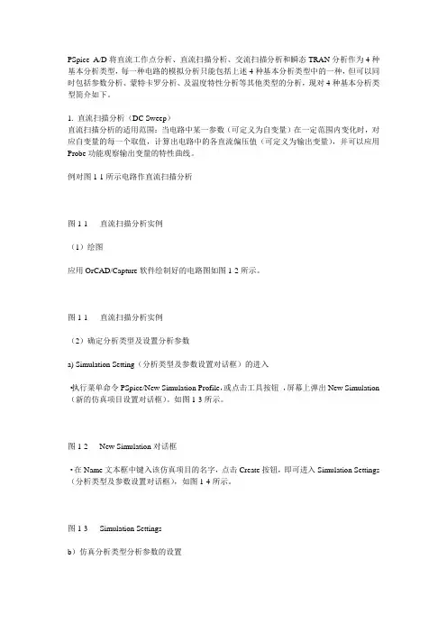
Pspice模型参数
附件A、三极管的Pspice模型参数.Model <model name> NPN(PNP、LPNP) [model parameters]
第 1 页共9页
第 2 页共9页
附件B、PSpice Goal Function
第 3 页共9页
附件C
Modeling voltage-controlled and temperature-dependent resistors
Analog Behavioral Modeling (ABM) can be used to model a nonlinear resistor through use of Ohm抯 law and tables and expressions which describe resistance. Here are some examples.
Voltage-controlled resistor
If a Resistance vs. Voltage curve is available, a look-up table can be used in the ABM expression. This table contains (Voltage, Resistance) pairs picked from points on the curve. The voltage input is nonlinearly mapped from the voltage values in the table to the resistance values. Linear interpolation is used between table values.
Let抯 say that points picked from a Resistance vs. Voltage curve are:
Voltage Resistance
The ABM expression for this is shown in Figure 1.
第 4 页共9页
Figure 1 - Voltage controlled resistor using look-up table
Temperature-dependent resistor
A temperature-dependent resistor (or thermistor) can be modeled with a look-up table, or an expression can be used to describe how the resistance varies with temperature. The denominator in the expression in Figure 2 is used to describe common thermistors. The TEMP variable in the expression is the simulation temperature, in Celsius. This is then converted to Kelvin by adding 273.15. This step is necessary to avoid a divide by zero problem in the denominator, when T=0 C.
NOTE: TEMP can only be used in ABM expressions (E, G devices).
Figure 3 shows the results of a DC sweep of temperature from -40 to 60 C. The y-axis shows the resistance or V(I1:-)/1A.
Figure 2 - Temperature controlled resistor
第 5 页共9页
Figure 3 - PSpice plot of Resistance vs. Temperature (current=1A)
Variable Q RLC network
In most circuits the value of a resistor is fixed during a simulation. While the value can be made to change for a set of simulations by using a Parametric Sweep to move through a fixed sequence of values, a voltage-controlled resistor can be made to change dynamically during a simulation. This is illustrated by the circuit shown in Figure 5, which employs a voltage-controlled resistor.
第 6 页共9页
Figure 4 - Parameter sweep of control voltage
This circuit employs an external reference component that is sensed. The output impedance equals the value of the control voltage times the reference. Here, we will use Rref, a 50 ohm resistor as our reference. As a result, the output impedance is seen by the circuit as a floating resistor equal to the value of V(Control) times the resistance value of Rref. In our circuit, the control voltage value is stepped from 0.5 volt to 2 volts in 0.5 volt steps, therefore, the resistance between nodes 3 and 0 varies from 25 ohms to 100 ohms in 25 ohm-steps.
第7 页共9页
Figure 5 - Variable Q RLC circuit
A transient analysis of this circuit using a 0.5 ms wide pulse will show how the ringing differs as the Q is varied.
Using Probe, we can observe how the ringing varies as the resistance changes. Figure 6 shows the input pulse and the voltage across the capacitor C1. Comparing the four output waveforms, we can see the most pronounced ringing occurs when the resistor has the lowest value and the Q is greatest. Any signal source can be used to drive the voltage-controlled resistance. If we had used a sinusoidal control source instead of a staircase, the resistance would have varied dynamically during the simulation.
第8 页共9页
Figure 6 - Output waveforms of variable Q RLC circuit
通过几天来的补习,我认为IS只是等于Icb0;
而VAF才是VCE0就是最高管耐压;
而IKF才是ICE0最大管电流;
BF是放大倍数没错了,
不知各位师傅有没有别的看法呢?
.MODEL MOD1 NPN IS=1E-6 BF=50 RB=100 V AF=160 CJC=3P 3DG201
第9 页共9页。
Pspice模型参数

附件A、三极管的Pspice模型参数.Model <model name> NPN(PNP、LPNP) [model parameters]第 1 页共9页第 2 页共9页附件B、PSpice Goal Function第 3 页共9页附件CModeling voltage-controlled and temperature-dependent resistorsAnalog Behavioral Modeling (ABM) can be used to model a nonlinear resistor through use of Ohm抯 law and tables and expressions which describe resistance. Here are some examples.Voltage-controlled resistorIf a Resistance vs. Voltage curve is available, a look-up table can be used in the ABM expression. This table contains (Voltage, Resistance) pairs picked from points on the curve. The voltage input is nonlinearly mapped from the voltage values in the table to the resistance values. Linear interpolation is used between table values.Let抯 say that points picked from a Resistance vs. Voltage curve are:Voltage ResistanceThe ABM expression for this is shown in Figure 1.第 4 页共9页Figure 1 - Voltage controlled resistor using look-up tableTemperature-dependent resistorA temperature-dependent resistor (or thermistor) can be modeled with a look-up table, or an expression can be used to describe how the resistance varies with temperature. The denominator in the expression in Figure 2 is used to describe common thermistors. The TEMP variable in the expression is the simulation temperature, in Celsius. This is then converted to Kelvin by adding 273.15. This step is necessary to avoid a divide by zero problem in the denominator, when T=0 C.NOTE: TEMP can only be used in ABM expressions (E, G devices).Figure 3 shows the results of a DC sweep of temperature from -40 to 60 C. The y-axis shows the resistance or V(I1:-)/1A.Figure 2 - Temperature controlled resistor第 5 页共9页Figure 3 - PSpice plot of Resistance vs. Temperature (current=1A)Variable Q RLC networkIn most circuits the value of a resistor is fixed during a simulation. While the value can be made to change for a set of simulations by using a Parametric Sweep to move through a fixed sequence of values, a voltage-controlled resistor can be made to change dynamically during a simulation. This is illustrated by the circuit shown in Figure 5, which employs a voltage-controlled resistor.第 6 页共9页Figure 4 - Parameter sweep of control voltageThis circuit employs an external reference component that is sensed. The output impedance equals the value of the control voltage times the reference. Here, we will use Rref, a 50 ohm resistor as our reference. As a result, the output impedance is seen by the circuit as a floating resistor equal to the value of V(Control) times the resistance value of Rref. In our circuit, the control voltage value is stepped from 0.5 volt to 2 volts in 0.5 volt steps, therefore, the resistance between nodes 3 and 0 varies from 25 ohms to 100 ohms in 25 ohm-steps.第7 页共9页Figure 5 - Variable Q RLC circuitA transient analysis of this circuit using a 0.5 ms wide pulse will show how the ringing differs as the Q is varied.Using Probe, we can observe how the ringing varies as the resistance changes. Figure 6 shows the input pulse and the voltage across the capacitor C1. Comparing the four output waveforms, we can see the most pronounced ringing occurs when the resistor has the lowest value and the Q is greatest. Any signal source can be used to drive the voltage-controlled resistance. If we had used a sinusoidal control source instead of a staircase, the resistance would have varied dynamically during the simulation.第8 页共9页Figure 6 - Output waveforms of variable Q RLC circuit通过几天来的补习,我认为IS只是等于Icb0;而VAF才是VCE0就是最高管耐压;而IKF才是ICE0最大管电流;BF是放大倍数没错了,不知各位师傅有没有别的看法呢?.MODEL MOD1 NPN IS=1E-6 BF=50 RB=100 V AF=160 CJC=3P 3DG201第9 页共9页。
PSpice04

第四讲
如果已知电路中某运放的宏模型及模型参 数,用户也可以自己创建该运放的模型。这里 将介绍两种最基本的线性运放模型:直流模型 和交流模型。
① 运放直流模型 运放直流模型可以等效为一个电压控制电 压源电路,如图1-23(a)所示,输入电阻Ri很大, 输出电阻Ro很小。Ri的典型值取2MegΩ,Ro的 典型值取75Ω。理想运放的输出电阻为零,模 型可简化为图1-23(b)所示电路。运放直流模型 适用于运放的直流和低频分析。
第四讲
而对于非线性元件本身,只需考虑与直流 工作状态有关的参数,如晶体管中电荷存储效 应则不必考虑。因此不同的分析要求需要建立 不同的等效模型。
由于实际电路元件的特性参数常常受集成 制造工艺和环境温度等诸多因素的影响,实际 参数值与理想的参数远远满足不了模拟要求。 因此,对许多元器件符号来说,除定义属性外, 还必须引入适当的电路模型、数学模型或物理 模型,通过定义相应的模型参数,才能反映各 种因素对元器件特性的影响,更准确地模拟实 际元器件的性能。
式中,IS—反向饱合电流(A); q—电子电荷量(1.6022E-19 C); K—波尔兹曼常数(1.3806E-23J/K); T—绝对温度(273.16K=0℃); n—发射系数,考虑PN不是突变结和载流子的 复合效应,n在1~2之间取值。二极管的符号与 模型如图1-21(b)所示。
第四讲
PSpice中二极管的模型参数共有14个,这 些参数的符号、含义和缺省值如表1-6所示。
第四讲
调频信号源:VSFFM、ISFFM 上述信号源名称中,开头字母为“V”的表 示电压源,如VSIN为正弦电压源,开头字母为 “I”的表示电流源,如ISIN表示正弦电流源。 由于同种类型的电压源和电流源,其属性和使 用方法都是类似的,为简便起见,只介绍电压 源。 a. 直流电压源(VDC) 直流电压源的属性如图1-30所示:
pspice3(二极管及模型参数)

3
二极管D的模型参数
4
练习1:二极管特性分析
eg1:电路如图所示,二极管参数: Is=2E-12,Rs=2Ω,输入信号为直流电压源,求二极管 上端电压随电压源的变化情况(0-5V)
5
模型参数修改方法
选中电路图中的dbreak元件 Schematics的主菜单editmodel 选择弹出对话框中edit instance model(txt)
BUBBL E11 Nhomakorabea12
6
7
文本编辑法(*.cir)
DIODE CIRCUIT *circuit name V1 2 0 5V *net R1 2 1 1k D1 1 0 DMOD .MODEL DMOD D(IS=2E-12 RS=2) *model edit .OP .DC LIN V1 0 5 0.1 *simu setup .PROBE *draw result 2:Pspice A/D-open .END
半导体二极管
半导体是导电性能介于导体和半导体之间的物 体。在一定条件下可导电。
2
二极管的V-I 特性
i D I S (e
v D / VT
1)
正向导通压降:硅管约0.7V,锗管0.2V 反向饱和电流:硅管为纳安(10-9)级 锗管为微安(10-6)级
硅二极管2CP10的V-I 特性
锗二极管2AP15的V-I 特性
Test.cir 1:Run editor
8
练习2:整流电路
已知二极管参数:Is=1e-14,Rs=1Ω,输入信 号幅度为5V,频率为1KHz的正弦波,求输出电 压波形,用文本编辑法实现 V2 1 0 SIN 0 5 1k 0 0 0
9
PSpice16.5教程二(噪声分析、参数分析、温度分析)

4 V-
15
1 OS1
6 OUT
5 OS2 V+
V1
0
15
0
out
0
图 2-5 反相运算放大器
上图所用到的器件信息: 器件
电源 电阻 晶体管 地
模型
V1 V2 V3 R1 R2 U1 0
2、仿真参数设置
模型库
VDC/source VSIN/source R/analog
uA741/opamp 0/source
邮箱:cadence@ / qipingwang@
也可以使用对数坐标显示结果,点选 按钮,就可以得到土 2-10 的结果
1.0V
10uV 0Hz V(OUT)
0.2KHz
0.4KHz
0.6KHz Frequency
2、分析参数的设置
首先点选菜单 Pspice/Edit Simulation,或者点击 ,出现设置参数的界面,如图 2-2 所示。在图 2-2 界面中选择 AC Analysis,设置频率参数,频率范围 1kHz 到 100MHz。 然后点选 Enabled 的小方框,选中噪声分析。并根据图 2-2 所示进行设置。图中的设 置表示将整个电路中的噪声源都集中折算到独立源 V1 处,然后计算在等效的噪声源 的激励下,输出点 V(out)处的产生的噪声。
3、执行 PSpice 程序
图 2-2 噪声分析的参数设置
图 2-2 点击确定后,再点击仿真工具栏中的 ,运行仿真。这样又调出了 PSpice
的界面。选择菜单栏 Trace/Add Trace,或者点击 图标,在“Simulation Output variables”中找到“V(INOISE)”和“V(ONOISE)”,得到输入噪声的波形和输出噪声 的波形,同样还可以通过 Plot/Add Y Axis 增加 Y 轴显示 DB 表示的输入噪声和输出 噪声波形。结果如图 2-3 所示。
第三讲-器件模型参数的优化提取详解

元器件模型参数的优化提取微电子学院贾新章(2013. 11 )PSpice中的模型和模型参数库一、概述:为元器件建立模型参数的步骤二、采用Model Editor分组提取模型参数三、基于器件物理原理计算部分模型参数四、建立适用于高级分析的元器件模型参数描述五、元器件模型参数的综合优化提取。
六、为元器件模型描述建立元器件符号七、将新建模型设置为PSpice仿真可以调用的库文件一、概述:为元器件建立模型参数的步骤第一步:优化提取模型参数1、采用Model Editor分组提取模型参数;2、基于器件物理原理,计算部分模型参数;3、为元器件建立适用于高级分析的模型参数描述;4、采用PSpice/Optimizer进行一次综合优化提取。
(采用前面结果作为优化提取模型参数的最佳初值)第二步:建立供Capture绘制电路图调用的元器件符号第三步:将新建模型设置为PSpice仿真可以调用的库文件。
下面将分别介绍每一部分的操作方法。
PSpice中的模型和模型参数库一、概述:为元器件建立模型参数的步骤二、采用Model Editor分组提取模型参数三、基于器件物理原理计算部分模型参数四、建立适用于高级分析的元器件模型参数描述五、元器件模型参数的综合优化提取。
六、为元器件模型描述建立元器件符号七、将新建模型设置为PSpice仿真可以调用的库文件二、采用Model Editor分组提取模型参数Model Editor模块可以对其支持的几种元器件,依据元器件的各种端特性数据,分组优化提取相应当模型参数数据。
(1) 调用MODEL EDITOR模块;(2) 选择执行Model/New命令,从对话框中设置模型类型。
下面以提取双极型晶体管模型参数为例(3)完成设置之后,点击OK,窗口就会更新为参数提取界面,不同的模型类型所对应的界面不相同,但界面的结构形式是一样的,分为三个子窗口。
特性数据输入窗口模型列表窗口参数列表窗口(4) 分组提取各组模型参数:将测试得到的器件外部端特性数据分别输入相应的特性窗口,分组进行参数提取。
Pspice仿真类型及不同电源参数
VSFFM属性设置框中各项参数的含义及单位见表1-3。
表1-3 VSFFM的属性参数
参数
含义
单位
VOFF
直流偏移电压
伏特
VAMPL
振幅
伏特
FC
载波频率
赫兹
FM
调制频率
赫兹
MOD
调制因子
无
按图1-15设置参数的VSFFM波形如图1-16所示。
图1-9 VSFFM波形
e)指数信号(VEXP、IEXP)
设置完毕,点击确定按钮。
图1-10 Simulation Settings
3.进行电路仿真
(1)执行菜单命令PSpice/Run,或点击工具按钮,调用PSpice A/D软件对该电路图进行仿真模拟。
(2)依次点击工具按钮、、,则电路图上相应位置依次显示节点电压、支路电流及各元器件上的功率损耗。如图1-29所示。
以上各项填完之后,按确定按钮,即可完成仿真分析类型及分析参数的设置。
另外,如果要修改电路的分析类型或分析参数,可执行菜单命令PSpice/Edit Simulation Profile,或点击工具按钮,在弹出的对话框中作相应修改。
(3)电路的模拟仿真
a)PSpice A/D视窗的启动
执行菜单命令PSpice/Run,或点击工具按钮,即可启动PSpice A/D视窗执行电路的仿真模拟,并且系统可自动调用Probe模块,对模拟结果进行后处理,屏幕显示如图1-5所示。
图1-11 VEXP波形
l瞬态分析的应用
现在通过举例,来说明瞬态分析的应用方法。
例:图1-19所示电路的电压源为分段线性源,其波形如图1-20所示。试对该电路进行瞬态分析。
第二讲-PSpice中的器件模型和模型参数
PSpice中的模型和模型参数库一.PSpice中的模型参数库二.模型描述格式半导体器件模型描述格式子电路模型描述格式三.以已有模型为基础新建模型描述四.为实际元器件提取模型参数、建立模型描述3.模型类别(按照建模方式划分)(1) 元器件物理模型(2) 子电路宏模型(3) 黑匣子宏模型4. 目前研究的问题(1) 提高模型精度。
(2) 建立新器件的模型。
(3) 提高模型参数提取精度。
5.PSpice中的模型参数库(1) PSpice软件数据库中提供有三万多个元器件的模型参数;分别存放在一百多个模型参数库文件(扩展名为LIB);一.PSpice中的模型参数库5.PSpice中的模型参数库(1) PSpice软件数据库中提供有三万多个元器件的模型参数;分别存放在一百多个模型参数库文件(扩展名为LIB);每个模型参数库文件都对应有一个元器件符号库文件(以OLB为扩展名),存放不同元器件的符号图。
一.PSpice中的模型参数库5.PSpice中的模型参数库(1) PSpice软件数据库中提供有三万多个元器件的模型参数;分别存放在一百多个模型参数库文件(扩展名为LIB);每个模型参数库文件都对应有一个元器件符号库文件(以OLB为扩展名),存放不同元器件的符号图。
注意:这两类库文件存放的子目录不相同。
元器件符号库文件所在的路径元器件模型参数库文件所在的路径注意:只有上述库文件中的元器件符号才配置有模型参数一.PSpice中的模型参数库5.PSpice中的模型参数库(1) PSpice软件数据库中提供有三万多个元器件的模型参数;分别存放在一百多个模型参数库文件(扩展名为LIB);每个模型参数库文件都对应有一个元器件符号库文件(以OLB为扩展名),存放不同元器件的符号图。
注意:这两类库文件存放的子目录不相同。
(2) 用户绘制电路图时实际调用的是元器件符号库中的元器件符号图。
调用PSpice进行模拟仿真时软件自动从对应的模型参数库中调用相应的模型参数。
SPICE模型、命令介绍
SPICE模型、命令介绍SPICE模型、命令介绍下⾯列出常⽤SPICE器件的模型描述。
{ }中的参数是必须的,[ ]中的参数可选,{ }*中的参数需要重复。
此外,每个SPICE模型提供商可能会有其他的参数或命令。
DEVICE:1、C device - Capacitor.C{name} {+node} {-node} [{model}] {value} [IC={initial}]Examples:CLOAD 15 0 20pFCFDBK 3 33 CMOD 10pF IC=1.5v2、D device - Diode.D{name} {+node} {-node} {model} [area]Examples:DCLAMP 14 0 DMOD3、I device - Current Source.I{name} {+node} {-node} [[DC] {value}] [AC {mag} [{phase}]]Examples:IBIAS 13 0 2.3mAIAC 2 3 AC .001IPULSE 1 0 PULSE(-1mA 1mA 2ns 2ns 2ns 50ns 100ns)I3 26 77 AC 1 SIN(.002 .002 1.5MEG)4、J device - Junction FET.J{name} {d} {g} {s} {model} [{area]}Examples:JIN 100 1 0 JFAST5、K device - Inductor Coupling.K{name} L{name} { L{name} }* {coupling}Examples:KTUNED L3OUT L4IN .8KXFR1 LPRIM LSEC .996、L device - Inductor.L{name} {+node} {-node} [model] {value} [IC={initial}]Examples:LLOAD 15 0 20mHL2 1 2 .2e-6LSENSE 5 12 2uH IC=2mA7、M device - MOSFET.M{name} {d} {g} {s} {sub} {mdl} [L={value}] [W={value}] + [AD={value}] [AS={value}] + [PD={value}] [PS={value}]+ [NRD={value}] [NRS={value}]Examples:M1 14 2 13 0 PNOM L=25u W=12uM13 15 3 0 0 PSTRONG8、Q device - Bipolar Transistor.Q{name} {c} {b} {e} [{subs}] {model} [{area}]Examples:Q1 14 2 13 PNPNOMQ13 15 3 0 1 NPNSTRONG 1.59、R device - Resistor.R{name} {+node} {-node} [{model}] {value}Examples:RLOAD 15 0 2k10、S device - Voltage-Controlled Switch.S{name} {+node} {-node} {+control} {-control} {model}Examples:S12 13 17 2 0 SMOD11、T device - Transmission Line.T{name} {A+} {A-} {B+} {B-} Z0={value}[TD={val} | F={val}[NL={val}]]Examples:T1 1 2 3 4 Z0=220 TD=115nsT2 1 2 3 4 Z0=50 F=5MEG NL=0.512、V device - Voltage Source.V{name} {+node} {-node} [[DC] {value}] [AC {mag} [{phase}]]Examples:VBIAS 13 0 2.3mVV AC 2 3 AC .001VPULSE 1 0 PULSE(-1mV 1mV 2ns 2ns 2ns 50ns 100ns)V3 26 77 AC 1 SIN(.002 .002 1.5MEG)13、X device - Subcircuit Call.X{name} [{node}]* {subcircuit name}Examples:X12 100 101 200 201 DIFFAMPCONTROLLED SOURCES14、E device - Voltage Controlled V oltage Source VCVS.E{name} {+node} {-node} {+cntrl} {-cntrl} {gain}E{name} {+node} {-node} POL Y({value}) {{+cntrl} {-cntrl}}* {{coeff}}* Examples: EBUFF 1 2 10 11 1.0EAMP 13 0 POL Y(1) 26 0 50015、F device - Current Controlled Current Source CCCS.F{name} {+node} {-node} {vsource name} {gain}Examples:FSENSE 1 2 VSENSE 10.016、G device - Voltage Controlled Current Source VCCS.G{name} {+node} {-node} {+control} {-control} {gain}Examples:GBUFF 1 2 10 11 1.017、H device - Current Controlled V oltage Source CCVS.H{name} {+node} {-node} {vsource name} {gain}H{name} {+node} {-node} POL Y({value}) { {vsource name} }* {{coeff}}* Examples: HSENSE 1 2 VSENSE 10.0HAMP 13 0 POL Y(1) VIN 500INPUT SOURCES18、EXPONENTIALEXP( {v1} {v2} {trise_delay} {tau_rise} {tfall_delay} {tau_fall) )19、PULSEPULSE( {v1} {v2} {tdelay} {trise} {tfall} {width} {period} )20、PIECE WISE LINEARPWL( {time1} {v1} {time2} {v2} ... {time3} {v3} )21、SINGLE FREQUENCY FMSFFM( {voffset} {vpeak} {fcarrier} {mod_index} {fsignal} )22、SINE WA VESIN( {voffset} {vpeak} {freq} {tdelay} {damp_factor} {phase} )ANALOG BEHA VIORAL MODELING23、V ALUEE|G{name} {+node} {-node} V ALUE {expression}Examples:GMULT 1 0 V ALUE = { V(3)*V(5,6)*100 }ERES 1 3 VALUE = { I(VSENSE)*10K }24、TABLEE|G{name} {+node} {-node} TABLE {expression} = (invalue, outvalue)* Examples: ECOMP 3 0 TABLE {V(1,2)} = (-1MV 0V) (1MV, 10V)25、LAPLACEE|G{name} {+node} {-node} LAPLACE {expression} {s expression} Examples:ELOPASS 4 0 LAPLACE {V(1)} {10 / (s/6800 + 1)}26、FREQE|G{name} {+node} {-node} FREQ {expression} (freq, gain, phase)* Examples:EAMP 5 0 FREQ {V(1)} (1KZ, 10DB, 0DEG) (10KHZ, 0DB, -90DEG)27、POL YE|G{name} {+node} {-node} POL Y(dim) {inputs X} {coeff k0,k1,...} [IC=value] Examples:EAMP 3 0 POL Y(1) (2,0) 0 500EMULT2 3 0 POL Y(2) (1,0) (2,0) 0 0 0 0 1ESUM3 6 0 POL Y(3) (3,0) (4,0) (5,0) 0 1.2 0.5 1.2COEFFICIENTS28、POL Y(1)y = k0 + k1?X1 + k2?X1?X1 + k3?X1?X1?X1 + ...29、POL Y(2)y = k0 + k1?X1+ k2?X2 + k3?X1?X1+ k4?X2?X1 + k5?X2?X2+ k6?X1?X1?X1 + k7?X2?X1?X1 + k8?X2?X2?X1+ k9?X2? X2?X2 + ...30、POL Y(3)y = k0 + k1?X1 + k2?X2 + k3?X3 + k4?X1?X1 + k5?X2?X1 + k6?X3?X1+ k7?X2?X2+ k8?X2?X3 + k9?X3?X3 + ...STATEMENTS31、.AC - AC Analysis..AC [LIN][OCT][DEC] {points} {start} {end}Examples:.AC LIN 101 10Hz 200Hz.AC DEC 20 1MEG 100MEG32、.DC - DC Analysis..DC [LIN] {varname} {start} {end} {incr}.DC [OCT][DEC] {varname} {start} {end} {points}Examples:.DC VIN -.25 .25 .05.DC LIN I2 5mA -2mA 0.1mA VCE 10V 15V 1V 33、.FOUR - Fourier Analysis..FOUR {freq} {output var}*Examples:.FOUR 10KHz v(5) v(6,7)34、.IC - Initial Transient Conditions..IC { {vnode} = {value} }*Examples:.IC V(2)=3.4 V(102)=035、.MODEL – Device Model..MODEL {name} {type}Typename Devname DevtypeCAP Cxxx capacitorIND Lxxx inductorRES Rxxx resistorD Dxxx diodeNPN Qxxx NPN bipolarPNP Qxxx PNP bipolarNJF Jxxx N-channel JFETPJF Jxxx P-channel JFETNMOS Mxxx N-channel MOSFETPMOS Mxxx P-channel MOSFETVSWITCH Sxxx voltage controlled switch Examples:.MODEL RMAX RES (R=1.5 TC=.02 TC2=.005).MODEL QDRIV NPN (IS=1e-7 BF=30)36、.NODESET – Initial bias point guess..NODESET { {node}={value} }*Examples:.NODESET V(2)=3.4 V(3)=-1V37、.NOISE - Noise Analysis..NOISE {output variable} {name} [{print interval}] Examples:.NOISE V(5) VIN38、.PLOT – Plot Output..PLOT [DC][AC][NOISE][TRAN] [ [{output variable}*] Examples: .PLOT DC V(3) V(2,3) V(R1) I(VIN).PLOT AC VM(2) VP(2) VG(2)39、.PRINT – Print Output..PRINT [DC][AC][NOISE][TRAN] [{output variable}*] Examples: .PRINT DC V(3) V(2,3) V(R1) IB(Q13).PRINT AC VM(2) VP(2) VG(5) II(7)40、.PROBE – Save simulation output PSPICE COMMAND. .PROBE [output variable]*Examples:.PROBE.PROBE V(3) VM(2) I(VIN)41、.SENS - Sensitivity Analysis..SENS {output variable}*Examples:.SENS V(9) V(4,3) I(VCC)42、.SUBCKT - Subcircuit Definition..SUBCKT {name} [{node}*]Examples:.SUBCKT OPAMP 1 2 101 10243、.TEMP – Temperature Analysis..TEMP {value}*Examples:.TEMP 0 27 12544、.TF – DC Transfer Function..TF {output variable} {input source name}Examples:.TF V(5) VIN45、.TRAN - Transient Analysis..TRAN {print step value} {final time} [{no print time} [{step ceiling value}]] [UIC] Examples:.TRAN 5NS 100NS。
关于PSPICE仿真软件中如何使用PARAMETERS参数分析教程
关于PSPICE仿真软件中如何使用PARAMETERS参数分析教程利用PARAMETERS进行参数分析,能够很好的分析参数变化所引起的波形变化,从而迅速观察出所需参数的范围值。
掌握此方法能够帮助我们高效率的完成工作。
接下来让我们看一下PARAMETERS参数分析使用的具体方法。
我们以一个TL431的分路稳压器的电路我为基础了解如何运用参数分析功能。
首先建立一个简单的原理图。
如上图所示,利用TL431的可编程性,调整R1,R2的比例关系,我们可以得到一个≤36V的输出电压,即Vout=Vvef(1+R2/R1)。
接下来我们看下此点路的波形,在原理图上我们添加两个电压探针。
仿真波形如下图所示:从波形中我们可以看出,Vref=2.4912V ,Vout=4.9845V。
从而验证了Vout=Vref(1+R2/R1),从例子中我们看出仿真软件给我们带来的便利。
接下来我们进入主题,学习如何运用PARAMETERS进行参数分析。
首先我们如下图搜索PARAM,选定PARAM/SPECIAL放在原理图上。
接下来我们就针对上图中的PARAMETERS进行相关的设置,设置之前要明确我们的目的,就是通过改变R2的值,来观察输出曲线的变化。
所以我们要做的工作就是把PARAMETERS进行关联。
1、双击PARAMETERS进行Property Editor设定。
2、在新打开的窗口中点击New Column…设置相关参数,var为任意起的一个名字,1k为R2现在的阻值。
3、双击R2的值1k进行关联设置。
此处的Value要与PARAM设置相互关联,此处我设置为{var}4、接下来我们进行仿真的相关设置。
设置参数如下图,注意全局变量Parameter name的设置。
5、点击仿真按钮,我们会看到如下对话框,点击OK。
6、我们可以观察到的仿真图形如下:参考电压不变,输出电压根据我们的设定显示出了不同的值。
方便我们对参数选取。
功能的实现基本就介绍到这里,如有疑问请联系我!hanjping@Hanjping at OPPLE2011.2.18。
bjt_model参数解释剖析
附件A、三极管的Pspice模型参数.Model <model name> NPN(PNP、LPNP) [model parameters]第 1 页共9页第 2 页共9页附件B、PSpice Goal Function第 3 页共9页附件CModeling voltage-controlled and temperature-dependent resistorsAnalog Behavioral Modeling (ABM) can be used to model a nonlinear resistor through use of Ohm抯 law and tables and expressions which describe resistance. Here are some examples.Voltage-controlled resistorIf a Resistance vs. Voltage curve is available, a look-up table can be used in the ABM expression. This table contains (Voltage, Resistance) pairs picked from points on the curve. The voltage input is nonlinearly mapped from the voltage values in the table to the resistance values. Linear interpolation is used between table values.Let抯 say that points picked from a Resistance vs. Voltage curve are:Voltage ResistanceThe ABM expression for this is shown in Figure 1.第 4 页共9页Figure 1 - Voltage controlled resistor using look-up tableTemperature-dependent resistorA temperature-dependent resistor (or thermistor) can be modeled with a look-up table, or an expression can be used to describe how the resistance varies with temperature. The denominator in the expression in Figure 2 is used to describe common thermistors. The TEMP variable in the expression is the simulation temperature, in Celsius. This is then converted to Kelvin by adding 273.15. This step is necessary to avoid a divide by zero problem in the denominator, when T=0 C.NOTE: TEMP can only be used in ABM expressions (E, G devices).Figure 3 shows the results of a DC sweep of temperature from -40 to 60 C. The y-axis shows the resistance or V(I1:-)/1A.Figure 2 - Temperature controlled resistor第 5 页共9页Figure 3 - PSpice plot of Resistance vs. Temperature (current=1A)Variable Q RLC networkIn most circuits the value of a resistor is fixed during a simulation. While the value can be made to change for a set of simulations by using a Parametric Sweep to move through a fixed sequence of values, a voltage-controlled resistor can be made to change dynamically during a simulation. This is illustrated by the circuit shown in Figure 5, which employs a voltage-controlled resistor.第 6 页共9页Figure 4 - Parameter sweep of control voltageThis circuit employs an external reference component that is sensed. The output impedance equals the value of the control voltage times the reference. Here, we will use Rref, a 50 ohm resistor as our reference. As a result, the output impedance is seen by the circuit as a floating resistor equal to the value of V(Control) times the resistance value of Rref. In our circuit, the control voltage value is stepped from 0.5 volt to 2 volts in 0.5 volt steps, therefore, the resistance between nodes 3 and 0 varies from 25 ohms to 100 ohms in 25 ohm-steps.第7 页共9页Figure 5 - Variable Q RLC circuitA transient analysis of this circuit using a 0.5 ms wide pulse will show how the ringing differs as the Q is varied.Using Probe, we can observe how the ringing varies as the resistance changes. Figure 6 shows the input pulse and the voltage across the capacitor C1. Comparing the four output waveforms, we can see the most pronounced ringing occurs when the resistor has the lowest value and the Q is greatest. Any signal source can be used to drive the voltage-controlled resistance. If we had used a sinusoidal control source instead of a staircase, the resistance would have varied dynamically during the simulation.第8 页共9页Figure 6 - Output waveforms of variable Q RLC circuit第9 页共9页。