SiT9005数据手册-1–141MHz任意频率SiTime扩频单端振荡器
SiT8008数据手册-SiTime低功耗1-110MHz任意频率单端有源晶振
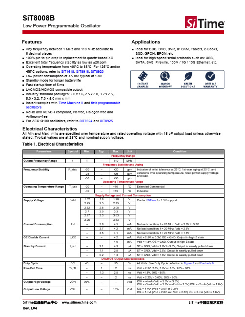
Electrical Characteristics
All Min and Max limits are specified over temperature and rated operating voltage with 15 pF output load unless otherwise stated. Typical values are at 25°C and nominal supply voltage.
+50 ppm Operating Temperature Range +70 °C
Hale Waihona Puke – +85 °C Industrial Supply Voltage and Current Consumption 1.8 2.5 2.8 3.0 3.3 – 3.8 3.7 3.5 – – 2.1 1.1 1.98 2.75 3.08 3.3 3.63 3.63 4.5 4.2 4.1 4.2 4.0 4.3 2.5 V V V V V V mA mA mA mA mA A A Contact SiTime for 1.5V support
Table 2. Pin Description
Pin Symbol Output Enable 1 OE/ST/NC Standby No Connect 2 3 4 GND OUT VDD Power Output Power Functionality H[1]: specified frequency output L: output is high impedance. Only output driver is disabled. H[1]: specified frequency output L: output is low (weak pull down). Device goes to sleep mode. Supply current reduces to I_std. Any voltage between 0 and Vdd or Open[1]: Specified frequency output. Pin 1 has no function. Electrical ground Oscillator output Power supply voltage[2] OE/ST/NC
SiT3809数据手册-80-220 MHz任意频率SiTime压控振荡器,牵引范围最大±1600ppm

FeaturesApplications⏹Any frequency between 80.000001 MHz and 220 MHz with 6 decimal places of accuracy⏹Telecom clock synchronization, instrumentation⏹Low bandwidth analog PLL, jitter cleaner, clock recovery, audio ⏹100% pin-to-pin drop-in replacement to quartz-based VCXO ⏹Video, 3G/HD-SDI, FPGA, broadband and networking⏹Frequency stability as tight as ±10 ppm⏹Widest pull range options from ±25 ppm to ±1600 ppm ⏹Industrial or extended commercial temperature range⏹Superior pull range linearity of ≤1%, 10 times better than quartz ⏹LVCMOS/LVTTL compatible output⏹Four industry-standard packages: 2.5 mm x 2.0 mm (4-pin),3.2 mm x 2.5mm (4-pin), 5.0 mm x 3.2 mm (6-pin), 7.0 mm x 5.0 mm (6-pin)⏹Instant samples with Time Machine II and field programmableoscillators⏹RoHS and REACH compliant, Pb-free, Halogen-free and Antimony-freeElectrical SpecificationsTable 1. Electrical Characteristics [1, 2, 3]ParameterSymbolMin.Typ.Max.Unit ConditionFrequency Range Output Frequency Range f 80.000001–220MHz Frequency Stability and AgingFrequency StabilityF_stab-10–+10ppm Inclusive of Initial tolerance [4] at 25°C, and variation over temperature, rated supply voltage and load.-25–+25ppm -50–+50ppm AgingF_aging -5–+5ppm 10 years, 25°C Operating Temperature RangeT_use-20–+70°C Extended Commercial -40–+85°C IndustrialSupply Voltage and Current ConsumptionSupply VoltageVdd1.71 1.8 1.89V Additional supply voltages between2.5V and3.3V can be supported. Contact SiTime for additional information.2.25 2.5 2.75V 2.52 2.8 3.08V 2.973.3 3.63V Current Consumption Idd –3436mA No load condition, f = 100 MHz, Vdd = 2.5V, 2.8V or 3.3V –3033mA No load condition, f = 100 MHz, Vdd = 1.8VStandby CurrentI_std––70μA Vdd = 2.5V, 2.8V, 3.3V, ST = GND, output is Weakly Pulled Down ––10μA Vdd = 1.8V, ST = GND, output is Weakly Pulled Down VCXO CharacteristicsPull Range [5, 6]PR ±25, ±50, ±100, ±150, ±200,±400, ±800, ±1600ppm See the Absolute Pull Range and APR table on page 8Upper Control VoltageVC_U1.7––V Vdd = 1.8V, Voltage at which maximum deviation is guaranteed.2.4––V Vdd = 2.5V, Voltage at which maximum deviation is guaranteed.2.7––V Vdd = 2.8V, Voltage at which maximum deviation is guaranteed.3.2––V Vdd = 3.3V, Voltage at which maximum deviation is guaranteed.Lower Control VoltageVC_L ––0.1V Voltage at which minimum deviation is guaranteed.Control Voltage Input Impedance Z_in 100––kΩControl Voltage Input Capacitance C_in –5–pF LinearityLin –0.11%Frequency Change Polarity –Positive slope–Control Voltage Bandwidth (-3dB)V_BW–8–kHzContact SiTime for 16 kHz and other high bandwidth optionsNotes:1.All electrical specifications in the above table are specified with 15 pF output load and for all Vdd(s) unless otherwise stated.2.The typical value of any parameter in the Electrical Characteristics table is specified for the nominal value of the highest voltage option for that parameter and at 25°C temperature.3.All max and min specifications are guaranteed across rated voltage variations and operating temperature ranges, unless specified otherwise4.Initial tolerance is measured at Vin = Vdd/25.Absolute Pull Range (APR) is defined as the guaranteed pull range over temperature and voltage.6.APR = pull range (PR) - frequency stability (F_stab) - Aging (F_aging)Electrical Specifications (continued)Table 1. Electrical Characteristics [1, 2, 3]ParameterSymbol Min.Typ.Max.Unit ConditionLVCMOS Output CharacteristicsDuty Cycle DC 45–55% f <= 165 MHz, all Vdds. Refer to Note 11 for definition of Duty Cycle.40–60% f > 165 MHz, all Vdds. Refer to Note 11 for definition of Duty Cycle . Rise/Fall Time Tr, Tf – 1.52ns Vdd = 1.8V, 2.5V, 2.8V or 3.3V, 10% - 90% Vdd level Output High VoltageVOH90%––VddIOH = -7 mA (Vdd = 3.0V or 3.3V)IOH = -4 mA (Vdd = 2.8V or 2.5V) IOH = -2 mA (Vdd = 1.8V)Output Low Voltage VOL ––10%VddIOL = 7 mA (Vdd = 3.0V or 3.3V)IOL = 4 mA (Vdd = 2.8V or 2.5V)IOL = 2 mA (Vdd = 1.8V)Input CharacteristicsInput Pull-up Impedance Z_in –100250kΩFor the OE/ST pin for 6-pin devices Input Capacitance C_in –5–pF For the OE/ST pin for 6-pin devicesStartup and Resume TimingStartup TimeT_start ––10ms See Figure 7 for startup resume timing diagramOE Enable/Disable Time T_oe ––115ns f = 80.000001 MHz, all Vdds. For other freq, T_oe = 100 ns + 3clock periodsResume Time T_resume –710msSee Figure 8 for resume timing diagram JitterRMS Period JitterT_jitt – 1.52ps f = 156.25 MHz, Vdd = 2.5V, 2.8V or 3.3V –23ps f = 156.25 MHz, Vdd = 1.8VRMS Phase Jitter (random)T_phj–0.51ps f = 156.25 MHz, Integration bandwidth = 12 kHz to 20 MHzTable 2. Pin Description. 4-Pin Configuration(For 2.5 x 2.0 mm and 3.2 x 2.5 mm packages)Pin Symbol Functionality1VIN Input 0-Vdd: produces voltage dependent frequency change2GND Power Electrical ground 3CLK Power Power supply voltage 4VDDInput PowerOscillator output power [7]Note:7. A capacitor value of 0.1 µF between VDD and GND is recommended.Table 3. Pin Description. 6-Pin Configuration(For 5.0 x 3.2 mm and 7.0 x 5.0 mm packages)Pin Symbol Functionality1VINInput 0-Vdd: produces voltage dependent frequency change 2NC/OE/ STNo ConnectH or L or Open: No effect on output frequency or other device functionsOutput Enable H or Open [8]: specified frequency output L: output is highStandbyH or Open [8]: specified frequency outputL: output is low (weak pull down)[9]. Oscillation stops 3GND Power Electrical ground 4CLK Output Oscillator output5NC No Connect H or L or Open: No effect on output frequency or other device functions6VDDPowerPower supply voltage [10]Notes:8. In OE or ST mode, a pull-up resistor of 10 kΩ or less is recommended if pin 2 in the 6-pin package is not externally driven. If pin 2 needs to be left floating, use the NC option9. Typical value of the weak pull-down impedance is 5 mΩ10. A capacitor value of 0.1 µF between VDD and GND is recommended.Table 4. Absolute Maximum LimitsAttempted operation outside the absolute maximum ratings may cause permanent damage to the part. Actual performance of the IC is only guaranteed within the operational specifications, not at absolute maximum ratings.ParameterMin.Max.Unit Storage Temperature -65150°C VDD-0.54V Electrostatic Discharge–2000V Soldering Temperature (follow standard Pb free soldering guidelines)–260°CTable 5. Thermal ConsiderationParameter θJA, 4 Layer Board(°C/W)θJA, 2 Layer Board(°C/W)θJC, Bottom(°C/W)70501912633050329719924322510921227252011722226Table 6. Environmental ComplianceParameterCondition/Test MethodMechanical Shock MIL-STD-883F, Method 2002Mechanical Vibration MIL-STD-883F, Method 2007Temperature Cycle JESD22, Method A104SolderabilityMIL-STD-883F, Method 2003Moisture Sensitivity LevelMSL1 @ 260°CTop ViewNotes:11.Duty Cycle is computed as Duty Cycle = TH/Period.12.SiT3809 supports the configurable duty cycle feature. For custom duty cycle at any given frequency, contact SiTime .Phase Noise PlotFigure 3. Phase NoiseTest Circuit and WaveformFigure 4. Test Circuit (4-Pin Device)Figure 5. Test Circuit (6-Pin Device)Figure 6. WaveformTiming DiagramFigure 7. Startup Timing (OE/ST Mode)Figure 8. Standby Resume Timing (ST Mode Only)Figure 9. OE Enable Timing (OE Mode Only)Figure 10. OE Disable Timing (OE Mode Only)Notes:13. SiT3809 supports “no runt” pulses and “no glitch” output during startup or resume.14. SiT3809 supports gated output which is accurate within rated frequency stability from the first cycle.Instant Samples with Time Machine and Field Programmable OscillatorsSiTime supports a field programmable version of the SiT3809MEMS VCXO for fast prototyping and real time customization of features. The field programmable devices (FP devices) are available for all four standard SiT3809 package sizes and can be configured to one’s exact specification using the Time Machine II , an USB powered MEMS oscillator programmer. Customizable Features of the SiT3809 FP Devices Include •Any frequency between 80.000001 MHz to 220 MHz •Three frequency stability options: ±10 ppm, ±25 ppm,±50 ppm•Two operating temperatures: -20 to 70°C or -40 to 85°C •Four supply voltage options: 1.8V, 2.5V, 2.8V, and 3.3V •Eight pull range options: ±25 ppm, ±50 ppm, ±100 ppm,±150 ppm, ±200 ppm, ±400 ppm, ±800 ppm, ±1600 ppmFor more information regarding SiTime’s field programmable solutions, visit /time-machine and /fp-devices .SiT3809 is typically factory-programmed per customer ordering codes for volume delivery.Note:15.Top marking: Y denotes manufacturing origin and XXXX denotes manufacturing lot number. The value of “Y” will depend on the assembly location of the device.Dimensions and PatternsOrdering InformationNote:16. Contact SiTime for different drive strength to drive multiple loads or to reduce EMI.Note:17.“–” indicates “not available.”Table 7. APR DefinitionAbsolute pull range (APR) = Norminal pull range (PR) - frequency stability (F_stab) - Aging (F_aging)Frequency StabilityNominal Pull Range± 10± 25± 50APR (PPM)± 25± 10––± 50± 35± 20–± 100± 85± 70± 45± 150± 135± 120± 95± 200± 185± 170± 145± 400± 385± 370± 345± 800± 785± 770± 745± 1600± 1585± 1570± 1545Table 8. Ordering Codes for Supported Tape & Reel Packing Method [17]Device Size 12 mm T&R (3ku)12 mm T&R (1ku)8 mm T&R (3ku)8 mm T&R 1ku)2.5 x 2.0 mm ––D E3.2 x 2.5 mm ––D E 5.0 x 3.2 mm T Y ––7.0 x 5.0 mmTY––© SiTime Corporation 2015. The information contained herein is subject to change at any time without notice. SiTime assumes no responsibility or liability for any loss, damage or defect of a Product which is caused in whole or in part by (i) use of any circuitry other than circuitry embodied in a SiTime product, (ii) misuse or abuse including static discharge, neglect or accident, (iii)unauthorized modification or repairs which have been soldered or altered during assembly and are not capable of being tested by SiTime under its normal test conditions, or (iv) improper installation, storage, handling, warehousing or transportation, or (v) being subjected to unusual physical, thermal, or electrical stress.Disclaimer: SiTime makes no warranty of any kind, express or implied, with regard to this material, and specifically disclaims any and all express or implied warranties, either in fact or by operation of law, statutory or otherwise, including the implied warranties of merchantability and fitness for use or a particular purpose, and any implied warranty arising from course of dealing or usage of trade, as well as any common-law duties relating to accuracy or lack of negligence, with respect to this material, any SiTime product and any product documentation. Products sold by SiTime are not suitable or intended to be used in a life support application or component, to operate nuclear facilities, or in other mission critical applications where human life may be involved or at stake. All sales are made conditioned upon compliance with the critical uses policy set forth below.CRITICAL USE EXCLUSION POLICYBUYER AGREES NOT TO USE SITIME'S PRODUCTS FOR ANY APPLICATION OR IN ANY COMPONENTS USED IN LIFE SUPPORT DEVICES OR TO OPERATE NUCLEAR FACILITIES OR FOR USE IN OTHER MISSION-CRITICAL APPLICATIONS OR COMPONENTS WHERE HUMAN LIFE OR PROPERTY MAY BE AT STAKE.SiTime owns all rights, title and interest to the intellectual property related to SiTime's products, including any software, firmware, copyright, patent, or trademark. The sale of SiTime products does not convey or imply any license under patent or other rights. SiTime retains the copyright and trademark rights in all documents, catalogs and plans supplied pursuant to or ancillary to the sale of products or services by SiTime. Unless otherwise agreed to in writing by SiTime, any reproduction, modification, translation, compilation, or representation of this material shall be strictly prohibited.Table 9. Additional InformationDocument DescriptionDownload LinkManufacturing Notes Tape & Reel dimension, reflow profile and other manufacturing related info /component/docman/doc_download/85-manufaturing-notes-for-sitime-oscillatorsQualification Reports RoHS report, reliability reports, composition reports/support/quality-and-reliabilityPerformance ReportsAdditional performance data such as phase noise, current consumption and jitter for selected frequencies /support/performance-measurement-reportTermination Techniques Termination design recommendations /support/application-notes Layout Techniques Layout recommendations /support/application-notesVCXOSpecifications Definition of key VCXO specifications such as APR and Kv/support2/documents/AN10020_VCXO_SpecDefinitions_rev1.pdfVCXO in PLL DesignSelection of VCXO parameters and trade-offs in PLL designs/support2/documents/AN10021_VCXO_PLL_Design_Guidelines_1v0.pdfRevision HistoryTable 10. Datasheet Version and Change LogVersion Release Date Change Summary 0.61/24/2013Preliminary 1.03/18/14•Preliminary removed from title •Updated features and application •Updated electrical specifications table •Updated figure 4,•Added new 6-pin device for figure 5•Updated timing diagrams•Updated ordering information drawing •Updated APR table•Updated ordering codes for tape and reel table •Reformatted additional information table columns1.011/8/15•Corrected CLK and VDD functionality description in Table 2•Revised VIN functionality description in Table 3Supplemental Information The Supplemental Information section is not part of the datasheet and is for informational purposes only.Silicon MEMS Outperforms QuartzBest ReliabilitySilicon is inherently more reliable than quartz. Unlike quartz suppliers, SiTime has in-house MEMS and analog CMOS expertise, which allows SiTime to develop the most reliable products. Figure 1 shows a comparison with quartz technology.Why is SiTime Best in Class:•SiTime’s MEMS resonators are vacuum sealed using an advanced EpiSeal™ process, which eliminates foreign par-ticles and improves long term aging and reliability •World-class MEMS and CMOS design expertiseFigure 1. Reliability Comparison [1]Best AgingUnlike quartz, MEMS oscillators have excellent long term aging performance which is why every new SiTime product specifies 10-year aging. A comparison is shown in Figure 2.Why is SiTime Best in Class:•SiTime’s MEMS resonators are vacuum sealed using an advanced EpiSeal process, which eliminates foreign parti-cles and improves long term aging and reliability •Inherently better immunity of electrostatically driven MEMS resonatorFigure 2. Aging Comparison [2]Best Electro Magnetic Susceptibility (EMS)SiTime’s oscillators in plastic packages are up to 54 times more immune to external electromagnetic fields than quartz oscillators as shown in Figure 3.Why is SiTime Best in Class:•Internal differential architecture for best common mode noise rejection•Electrostatically driven MEMS resonator is more immune to EMSFigure 3. Electro Magnetic Susceptibility (EMS)[3]Best Power Supply Noise RejectionSiTime’s MEMS oscillators are more resilient against noise on the power supply. A comparison is shown in Figure 4.Why is SiTime Best in Class:•On-chip regulators and internal differential architecture for common mode noise rejection•Best analog CMOS design expertiseFigure 4. Power Supply Noise Rejection [4]SiTime 20X Better1.53.53.08.02468101-Year 10-YearSiTime MEMS vs. Quartz AgingSiTime MEMS OscillatorQuartz OscillatorA g i n g (±P P M )SiTime 2X Better- 39- 40- 42- 43- 45- 73Kyocera Epson TXC CW SiLabs SiTimeSiTime 54X Better1,000Power Supply Noise Frequency (kHz)SiTime SiTime 3X BetterBest Vibration RobustnessHigh-vibration environments are all around us. All electronics,from handheld devices to enterprise servers and storage systems are subject to vibration. Figure 5 shows a comparison of vibration robustness.Why is SiTime Best in Class:•The moving mass of SiTime’s MEMS resonators is up to 3000 times smaller than quartz•Center-anchored MEMS resonator is the most robust designFigure 5. Vibration Robustness [5]Best Shock RobustnessSiTime’s oscillators can withstand at least 50,000 g shock.They all maintain their electrical performance in operation during shock events. A comparison with quartz devices is shown in Figure 6.Why is SiTime Best in Class:•The moving mass of SiTime’s MEMS resonators is up to 3000 times smaller than quartz•Center-anchored MEMS resonator is the most robust designFigure 6. Shock Robustness [6]Vibration Frequency (Hz)SiTime Up to 30x Better14.312.63.92.92.50.6Kyocera Epson TXC CW SiLabs SiTimeSiTime Up to 25x BetterNotes:1.Data Source: Reliability documents of named companies.2.Data source: SiTime and quartz oscillator devices datasheets.3.Test conditions for Electro Magnetic Susceptibility (EMS):• According to IEC EN61000-4.3 (Electromagnetic compatibility standard)• Field strength: 3V/m• Radiated signal modulation: AM 1 kHz at 80% depth • Carrier frequency scan: 80 MHz – 1 GHz in 1% steps • Antenna polarization: Vertical• DUT position: Center aligned to antenna Devices used in this test:SiTime, SiT9120AC-1D2-33E156.250000 - MEMS based - 156.25 MHz Epson, EG-2102CA 156.2500M-PHPAL3 - SAW based - 156.25 MHz TXC, BB-156.250MBE-T - 3rd Overtone quartz based - 156.25 MHz Kyocera, KC7050T156.250P30E00 - SAW based - 156.25 MHzConnor Winfield (CW), P123-156.25M - 3rd overtone quartz based - 156.25 MHz SiLabs, Si590AB-BDG - 3rd overtone quartz based - 156.25 MHz 4.50 mV pk-pk Sinusoidal voltage.Devices used in this test:SiTime, SiT8208AI-33-33E-25.000000, MEMS based - 25 MHz NDK, NZ2523SB-25.6M - quartz based - 25.6 MHzKyocera, KC2016B25M0C1GE00 - quartz based - 25 MHz Epson, SG-310SCF-25M0-MB3 - quartz based - 25 MHz5.Devices used in this test: same as EMS test stated in Note 3.6. Test conditions for shock test:• MIL-STD-883F Method 2002• Condition A: half sine wave shock pulse, 500-g, 1ms• Continuous frequency measurement in 100 μs gate time for 10 seconds Devices used in this test: same as EMS test stated in Note 37.Additional data, including setup and detailed results, is available upon request to qualified customers. Please contact productsupport@ .The Smart Timing Choice ™The Smart Timing Choice ™Document Feedback FormSiTime values your input in improving our documentation. Click here for our online feedback form or fill out and email the form below to productsupport@ .1.Does the Electrical Characteristics table provide complete information?Yes NoIf No, what parameters are missing?_________________________________________________________________________________________________2. Is the organization of this document easy to follow?YesNoIf “No,” please suggest improvements that we can make:_________________________________________________________________________________________________3.Is there any application specific information that you would like to see in this document? (Check all that apply)Shock and vibration performanceOtherIf “Other,” please specify:_________________________________________________________________________________________________4. Are there any errors in this document? YesNoIf “Yes”, please specify (what and where):_________________________________________________________________________________________________5.Do you have additional recommendations for this document?_________________________________________________________________________________________________Name ________________________________________________________________________________Title________________________________________________________________________________Company _________________________________________________________________________________________Address _________________________________________________________________________________________City / State or Province / Postal Code / Country ___________________________________________________________Telephone __________________________________Application ________________________________________________________________________________________Would you like a reply?YesNoThank you for your feedback. Please click the email icon in your Adobe Reader tool bar and send to productsupport@ .Or you may use our online feedback form .。
SiTime MEMS振荡器相位噪声测量指南

SiTime MEMS振荡器相位噪声测量指南1 简介相位噪声是振荡器的基本指标之一。
经验丰富的工程师可以通过查看相位噪声图来了解有关振荡器质量以及它是否适合应用的很多信息。
RF 工程师专注于某些载波偏移频率下的相位噪声水平,以确保可以支持所需的调制方案。
设计40GbE 等高速串行链路的专业人员将带通滤波器应用于参考时钟的相位噪声,对其进行积分,并将其转换为相位抖动以预测系统的误码率。
本应用指南首先简要介绍相位噪声和相位噪声测量方法的理论概述,然后重点介绍实用的相位噪声测量建议,例如将被测信号正确连接到仪器、设置相位噪声分析仪以及选择合适的相位噪声分析仪。
设置。
本文档中的所有测量均使用Keysight E5052B 相位噪声分析仪进行,该分析仪是北美最常用的相位噪声测量仪器之一。
2 什么是相位噪声相位噪声是信号短期相位不稳定性的频域表示。
相位噪声通常被描述为单边带(SSB) 相位噪声并表示为L(f)。
相位噪声的经典定义是在载波偏移频率处测得的功率谱密度与信号总功率之比。
出于实际目的,此定义已稍作修改,以便在载波偏移频率处测量的功率谱密度以载波功率为参考,而不是以总积分信号功率为参考(图2-1)。
图2-1:经典相位噪声定义使用频谱分析仪测量相位噪声时,经典定义很方便,但它结合了幅度和相位噪声效应。
它还对具有高相位噪声的信号有限制。
经典定义通常适用于峰峰值相位偏差远小于1 弧度的信号。
它也永远不能大于0 dB,因为信号中的噪声功率不能大于信号的总功率。
最近,相位噪声被重新定义为相位波动L(f) = SΦ(f)/2 的功率谱密度的一半。
理想的正弦波可以表示为f(t) = A∙sin(ωt + φ)。
具有相位噪声的正弦波可以表示为f(t) =A∙sin(ωt + φ(t)),其中φ(t) 是相位噪声。
那么SΦ(f) 是φ(t) 的功率谱密度。
以这种方式定义时,相位噪声与幅度噪声是分开的。
它也可以大于0 dB,这意味着相位变化大于1 弧度。
Sitime产品选型手册中文2012
p p
p p
-
p p
-
压控振荡器 — VCXO
SiT3807 网络、电信、 医疗、ATE、 视频、xDSL、 及嵌入式系统 VCXO • 可选标准频率,最大程度降低 成本 • 超低相位抖动: 0.5 psrms • 最广牵引范围 • 1%牵引线性度 • 超低相位抖动: 0.5 psrms 1.5-45 (标准频点范围) 1-80 10, 25, 50 80-220 25, 50 25-200 (1%线性度) CMOS LVTTL 32 70 µA (待机) C, I 2.5x2.0 mm 3.2x2.5 mm 5.0x3.2 mm 7.0x5.0 mm
-
-
要求低EMI的计算机 设备应用 应用、服务器
SiT9002
SSXO
• 扩频设计: 中心展频或向下 展频
1-220
25, 50
-
LVPECL LVDS HCSL CML
48-75
C, I
5.0x3.2 mm 7.0x5.0 mm
p
p
-
p
差分压控振荡器 — VCXO
SiT3821 网络、电信、 医疗、ATE、 视频、xDSL、 嵌入式系统 SiT3822 VCXO • 最佳稳定度 • 1%牵引线性度 • 超低相位抖动: 0.5 psrms 220-625 1-220 10, 25, 50 25-1600 (1% 牵引线 性度) LVPECL LVDS 55-69 C, I 5.0x3.2 mm 7.0x5.0 mm
单端数控振荡器 — DCXO
网络及电信
SiT3907
DCXO
• 单引脚串口可编程 • 0.1% 牵引线性度动 • 超低相位抖动 0.5 psrms
Sitime MEMS硅晶振介绍
Confidential
7
硅晶振内部框图/温度补偿
Programmable Oscillator
MEMS Resonator
VDD
Oscillator
5MHz
Frac-N PLL
CLK
(1~800MHz)
Prog. frequency Temperature Sensor GND A/D Digital Temperature Compensation
OSC、震盪器、晶振、 有源晶振
長晶
切割 清洗、抛光
披银
測試 校正
封装、黏贴 氮气密封
老化 测试
测试 筛选
打标
卷带封装
自日系起振芯片厂商采购起振芯片以及基座
Confidential
4
石英振荡器与MEMS硅晶振的区别
石英振荡器
• • • 石英切割组合简单三极管电路,易受环境 影响(湿度、温度、震动等) 金属封装,存在气密性问题 人工切割,人工的参与质量不稳定,产能 扩充困难,每一个频点需要不同的晶片
SiTime整合 8 个供应商
Confidential
11
SiTime MEMS时脉产品价值和优势
SiTime可编程 MEMS振荡器
交货期 质量
库存管理及风险
2-4周 全自动生产,质量稳定
只需2-4周存货,节省库存成本
传统固定频率 石英振荡器
8-16周 人工切割,质量受工人素质影响
进货周期长,需存货不同频点,电压,等
SiTime 全硅 MEMS 时钟方案
可靠性更高、任意频点可编程、成本更低
Confidential
SiTime 概览
• 美国硅谷VC投资Fabless IC创业公司具有业界 唯一量产,Bosch验证成熟的MEMS时脉技术及 最小,最薄的封装(<0.30um) 2007年三季量产,无一客户产品质量问题 高性能可编程MEMS时脉产品支持低抖动,高 频率,展频,低功耗,差分输出,多锁相环 (PLL)、多输出频率等功能 在九大应用领域里(网通,通讯,消费,服务器等) 超过800个客户,1500个计划进行测试或量产 与石英振荡器比较,超短交货期(2周),24小时克 制化样品,10倍的质量稳定性及无温飘的烦恼 业界标准封装,焊接管脚,直接替代石英组件 全球硅机电时钟领导者,年出货超越三千五百 万,并以指数快速增长。
sit8103,1-110MHZ 输出,可编程振荡器
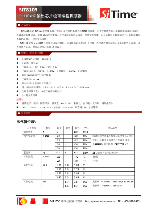
SiT8103/2是SiTime 最早推出的小体积,高性能的单端全硅MEMS 振荡器,用于对传统普通石英振荡器的升级与改造,无需改动PCB 设计,管脚100%完全兼容。
不仅可以降低产品成本,改善交货周期,而且从根本上有效解决了石英振荡器所伴随的温漂、一致性差等问题。
SiT8103支持1-110MHZ 任意频点可编程输出,且可精确到小数点后五位数。
内部具有温补功能,全温范围内无温漂,可直接替代石英,整体稳定度可提升10倍以上。
● 1-110MHZ 范围任一频点输出 ● 无温漂、低抖动● 工作电压:1.8V 、2.5V 、2.8V 、3.3V● 工作精度可达±20PPM 、±25PPM 、±30PPM 、±50PPM 、±100PPM ● 兼容LVCMOS/LVTTL 电平输出 ● 工作电流:6.1mA● 具有标准/使能两种工作模式● 同一频点多种封装:2.5×2.0,3.2×2.5,5.0×3.2,7.0×5.0mm ● 全硅半导体工艺,10倍于石英的稳定性 ● 2-4周交货周期应用:● 消费电子、视频、图像采集、机顶盒、HDTV 、DVR 、扫描仪、打印机、复印机、网络摄像头 ●USB1.1、USB2.0、SATA 、SAS 、光端机、IEEE 1394、以太网、PCI 总线等等电气特性表:工作参数 标识最小 典型 最大 单位 测试说明输出频率 f 1 - 110 MHZ频率稳定性F_stab -20 - +20 PPM 此处的精度指工作频偏、温度变化、电压变化、负载变化等条件下的综合考量。
±20PPM 仅限于商规(-20--+70℃)-25 - +25 PPM -30 - +30 PPM -50- +50 PPM老化率 Ag -1.0-+1.0ppM 25℃情况下每年的老化率 工作温度T_use-20 - +70 ℃ 商规 -40 - +85 ℃ 工规 工作电压 Vdd1.71 1.8 1.89 V2.25 2.5 2.75 V 2.52 2.83.08 V 2.973.3 3.63 V工作电流 Idd- 6.7 7.5 mA 无负载,f=20MHZ 、Vdd=2.5V,2.8V or 3.3V -6.16.7mA无负载,f=20MHZ 、Vdd=1.8V■ 特色,优点和应用 ■ 产品简介■ 技术参数工作参数标识最小典型最大单位测试说明静态电流I_std - 2.4 4.3 μA ST=GND, Vdd=3.3V, Output is WeaklyPulled Down- 1.2 2.2 μA ST = GND, Vdd = 2.5V or 2.8V, Output isWeakly Pulled Down- 0.4 0.8 μA ST=GND, Vdd=1.8V, Output is WeaklyPulled Down占空因数DC 45 50 55 % All Vdds. F<=75MHZ40 50 60 % All Vdds. F>75MHZ上升/下降时间Tr,Tf - 1 2 ns 20%--80% Vdd=2.5v,2.8v or 3.3v15pF Load- 1.3 2.5 ns 20%--80% Vdd=1.8v 15pF Load输出高电平VOH 90% - - Vdd IOH=-4mA (Vdd=3.3v)IOH=-3mA (Vdd=2.8v or 2.5v)IOH=-2mA (Vdd=1.8v)输出低电平VOL - - 10% Vdd IOL=4mA (Vdd=3.3v)IOL=3mA (Vdd=2.8v or 2.5v)IOL=2mA (Vdd=1.8v)输出负载Output load Ld - - 15PF At maximum frequency and supplyvoltage.Contact SiTime for higheroutput load option输入高电平VIH 70% - - Vdd Pin 1,OE or ST输入低电平VIL - - 30% Vdd Pin 1,OE or ST建立时间Startup TimeT_osc - - 10 ms 如下图1所示恢复时间Resume TimeT_resume - 3.0 4 ms 如下图1所示周期抖动T_jitt - - 4.0 ps f=75MHZ,Vdd=2.5V,2.8V or 3.3V- - 6.5 ps f=75MHZ,Vdd=1.8V相位抖动T_phj - 0.6 - ps f=75MHZ,测试带宽:900Khz to 7.5MHZ,Vdd=2.5V,2.8V or 3.3V.- 0.8 - ps f=75MHZ,测试带宽:900Khz to 7.5MHZ,Vdd=1.8V.图1管脚说明:OE 模式:当1脚为高或悬空时,正常输出CLK 信号; 当1脚为低时,输出禁止,呈高阻状态。
SiTime推出目前业界最小可编程扩频时钟振荡器系列产品
SiTime推出目前业界最小可编程扩频时钟振荡器系列产品
佚名
【期刊名称】《微纳电子技术》
【年(卷),期】2009(46)7
【摘要】MEMS Si计时设备领域的领衔企业SiTime最新推出了业界尺寸最小的
低周期到周期抖动宽频可编程扩频振荡器系列产品。
首款高性能产品包括
SiT9001和SiT9002。
SiT9001在业界空间占位堪称最小,适用于空间受限产品。
SIT9002是目前市场上唯一一款差分输出可编程扩频时钟振荡器。
这两款产品都
以内置MEMS谐振器作为时钟参考,而无需额外组件。
此外,两种产品都采用了SiTime成熟的MEMS技术,
【总页数】1页(P447-447)
【关键词】高性能产品;时钟振荡器;可编程;扩频;MEMS谐振器;MEMS技术;周期
抖动;差分输出
【正文语种】中文
【中图分类】TP316.7;TQ340.47
【相关文献】
1.Dallas推出扩频电阻可编程振荡器 [J],
2.赛普拉斯推出新型可编程FleXO时钟发生器系列产品 [J],
3.奥地利微电子推出具备降压功能的高效200mA DC-DC升压转换器/德州仪器推出业界最小正弦至正弦波时钟缓冲器 [J],
4.SiTime高精度MEMS振荡器颠覆全球电信与网络时钟市场 [J], 王颖
5.PMC-Sierra新推出maxSAS系列产品/Philips推出业界最小的4通道UART芯片 [J],
因版权原因,仅展示原文概要,查看原文内容请购买。
SiTime MEMS 振荡器产品数据手册说明书

SiTime introduced two families of ultra-robust AEC-Q100-qualified MEMS oscillators. The SiT2024/25 and SiT8924/25 oscillators deliver the highest performance and best robustness and are designed for ASIL (Automotive Safety Integrity Level) compliant automotive applications such as advanced driver assistance systems (ADAS), in-vehicle Ethernet, powertrain and electronic control units (ECUs).“The automotive industry is going through a massive transformation, with new features such as advanced safety and driver assistance systems, electrification, automation and real-time big data analytics. The usage of electronic components in automobiles is increasing rapidly and requires stringent levels of quality, reliability and performance,” said Piyush Sevalia, executive vice president of marketing at SiTime. “MEMS technologies are playing a significant role in this transformation. SiTime is leveraging our revolutionary silicon MEMS, advanced analog technology and standard semiconductor packaging to provide unique timing solutions that deliver the highest reliability and dynamic performance under extreme temperatures, shock and vibration.”SiTime’s new automotive product families offer a unique combination of the widest frequency range, tightest stability at ±20 ppm and the best reliability. The SiT2024/25 oscillators are optimized for under-the-hood systems such as engine control, transmission control, active suspension control, electronic steering and other ECUs. These oscillators are available in a SOT23-5 leaded package to enable visual inspection and the best solder joint reliability, especially in hot and cold environments. The SiT8924/25 oscillators, available in industry-standard QFN footprints as small as 2.0 x 1.6 mm, are ideal for camera modules and other small form factor systems.than quartz oscillators and deliver the following features and benefits.The SiT2024, SiT2025, SiT8924 and SiT8925 oscillators are in production now. Pricing information and Production Part Approval Process (PPAP) documentation, compliant with the AIAG manual, is available upon request.• AEC-Q100 qualified, Grade 1 (-40°C to +125°C), Grade 2 (-40°C to +105°C) and extended temperature range (-55°C to +125°C)3-wire version with a short-circuit protected open-drain output• SiT2024/2025: SOT23-5 leaded package for best board-level solder-joint reliability and ease-of-use in manufacturing and testLow current consumption of typ. 1.6 mA• SiT8924/8925: Five package options in industry-standard oscillator footprint• Excellent frequency stability at ±20 ppm for best timing margin• Highest reliability at over 1 billion hours MTBF (< 1 FIT)• Best shock resistance at 50,000 g• Best vibration resistance at 70 g• Lowest vibration sensitivity (g-sensitivity) at 0.1 ppb/g • Widest frequency range of 1 to 137 MHz with 6 decimal places of accuracy• Unique, programmable output drive strength for EMI reduction• Supply voltage options of 1.8 V, 2.5 to 3.3 VFEATURESHeadlightsEMI reductionSiT8924/5 & SiT2024/5AEC-Q100 MEMS Oscillator Applications & BenefitsPerformance in Presence of Vibration2016 2520 3225 5032 7050SOT23 SOIC-81. Contact SiTime for ≤±10 ppm stability options.2. Contact SiTime for AEC-Q100 compliance status.3. Contact SiTime for 95°C & 105°C products.。
- 1、下载文档前请自行甄别文档内容的完整性,平台不提供额外的编辑、内容补充、找答案等附加服务。
- 2、"仅部分预览"的文档,不可在线预览部分如存在完整性等问题,可反馈申请退款(可完整预览的文档不适用该条件!)。
- 3、如文档侵犯您的权益,请联系客服反馈,我们会尽快为您处理(人工客服工作时间:9:00-18:30)。
SiT90051 to 141 MHz EMI Reduction OscillatorFeatures⏹Spread spectrum for EMI reduction▪Wide spread % option▫Center spread: from ±0.125% to ±2%, ±0.125% step size ▫Down spread: -0.25% to -4% with -0.25% step size ▪Spread profile option: Triangular, Hershey-kiss⏹Programmable rise/fall time for EMI reduction: 8 options,0.25 to 40 ns⏹Any frequency between 1 MHz and 141 MHz accurate to 6 decimal places⏹ 100% pin-to-pin drop-in replacement to quartz-based XO’s ⏹ Excellent total frequency stability as low as ±20 ppm ⏹ Operating temperature from -40°C to 85°C.⏹ Low power consumption of 4.0 mA typical at 1.8V⏹ Pin1 modes: Standby, output enable, or spread disable ⏹ Fast startup time of 5 ms ⏹ LVCMOS output⏹Industry-standard packages▪QFN: 2.0 x 1.6, 2.5 x 2.0, 3.2 x 2.5 mm 2▪Contact SiTime for SOT23-5 (2.9 x 2.8 mm 2)⏹RoHS and REACH compliant, Pb-free, Halogen-free and Antimony-freeApplications⏹Surveillance camera ⏹IP camera⏹Industrial motors ⏹Flat panels⏹Multi function printers ⏹PCI expressElectrical SpecificationsTable 1. Electrical CharacteristicsAll Min and Max limits are specified over temperature and rated operating voltage with 15 pF output load unless otherwise stated. Typical values are at 25°C and 3.3V supply voltage.Table 1. Electrical Characteristics (continued)Table 2. Spread Spectrum % [1,2]Ordering Code Center Spread(%)Down Spread(%)A ±0.125 -0.25B ±0.250 -0.50C ±0.390 -0.78D ±0.515 -1.04E ±0.640 -1.29F ±0.765 -1.55G ±0.905 -1.84H ±1.030 -2.10I ±1.155 -2.36J ±1.280 -2.62K ±1.420 -2.91L ±1.545 -3.18M ±1.670 -3.45N ±1.795 -3.71O ±1.935 -4.01P ±2.060 -4.28Notes:1.In both center spread and down spread modes, modulation rateis employed with a frequency of ~31.25 kHz.2.Contact SiTime for wider spread options Table3. Spread ProfileSpread ProfileTriangularHershey-kissTable 4. Pin DescriptionTop ViewFigure 1. Pin AssignmentsNotes:3.In OE or ST mode, a pull-up resistor of 10 kΩ or less is recommended if pin 1 is not externally driven. If pin 1 needs to be left floating, use the NC option.4.A capacitor of value 0.1 µF or higher between Vdd and GND is required.Table 5. Absolute Maximum LimitsAttempted operation outside the absolute maximum ratings may cause permanent damage to the part.Actual performance of the IC is only guaranteed within the operational specifications, not at absolute maximum ratings.ParameterMin. Max. Unit Storage Temperature -65150 °C Vdd-0.54 V Electrostatic Discharge– 2000 V Soldering Temperature (follow standard Pb free soldering guidelines) – 260 °C Junction Temperature [5]–150°CNote:5.Exceeding this temperature for extended period of time may damage the device.Table 6. Maximum Operating Junction Temperature [6]Max Operating Temperature (ambient)Maximum Operating Junction Temperature70°C 80°C 85°C95°CNote:6.Datasheet specifications are not guaranteed if junction temperature exceeds the maximum operating junction temperature.Table 7. Environmental ComplianceParameterCondition/Test MethodMechanical Shock MIL-STD-883F, Method 2002 Mechanical Vibration MIL-STD-883F, Method 2007 Temperature Cycle JESD22, Method A104 SolderabilityMIL-STD-883F, Method 2003 Moisture Sensitivity LevelMSL1 @ 260°C12 34VDDOUTGND OE// NC/SDTiming DiagramsT_start: Time to start from power-offFigure 2. Startup TimingT_resume: Time to resume from STFigure 3. Standby Resume Timing(ST Mode O nly)T_oe: Time to re-enable the clock outputFigure 4. OE Enable Timing (OE Mode Only)T_oe: Time to put the output in High Z modeFigure 5. OE Disable Timing (OE Mode Only)F r e q u e n c yFigure 6. SD Enable Timing (SD Mode Only)F re q u e n c y D e v i a t i o n (%)Figure 7. SD Diable Timing (SD Mode Only)Note:7.SiT9005 has “no runt” pulses and “no glitch” output during startup or resume.Programmable Drive StrengthThe SiT9005 includes a programmable drive strength feature to provide a simple, flexible tool to optimize the clock rise/fall time for specific applications. Benefits from the programmable drive strength feature are:⏹Improves system radiated electromagnetic interference(EMI) by slowing down the clock rise/fall t ime⏹Improves the downstream clock receiver’s (RX) jitter bydecreasing (speeding up) the clock rise/fall t ime.⏹Ability to drive large capacitive loads while maintaining fullswing with sharp edge rates.For more detailed information about rise/fall time control and drive strength selection, see the SiTime Application Notes section: /support/application-notes.EMI Reduction by Slowing Rise/Fall TimeFigure 8 shows the harmonic power reduction as the rise/fall times are increased (slowed down). The rise/fall times are expressed as a ratio of the clock period. For the ratio of 0.05, the signal is very close to a square wave. For the ratio of 0.45, the rise/fall times are very close to near-triangular waveform. These results, for example, show that the 11th clock harmonic can be reduced by 35 dB if the rise/fall edge is increased from5% of the period to 45% of the period.Figure 8. Harmonic EMI reduction as a Functionof Slower Rise/Fall TimeJitter Reduction with Faster Rise/Fall TimePower supply noise can be a source of jitter for the downstream chipset. One way to reduce this jitter is to increase rise/fall time (edge rate) of the input clock. Some chipsets would require faster rise/fall time in order to reduce their sensitivity to this type of jitter. The SiT9005 provides up to 3 additional high drive strength settings for very fast rise/fall time. Refer to the Vdd = 1.8V Rise/Fall Times for Specific C LOAD to determine the proper drive strength.High Output Load CapabilityThe rise/fall time of the input clock varies as a function of the actual capacitive load the clock drives. At any given drive strength, the rise/fall time becomes slower as the output load increases. As an example, for a 3.3V SiT9005 device with default drive strength setting, the typical rise/fall time is 1.1 ns for 15 pF output load. The typical rise/fall time slows down to 2.9 ns when the output load increases to 45 pF. One can choose to speed up the rise/fall time to 1.9 ns by then increasing the drive strength setting on the SiT9005. The SiT9005 can support up to 60 pF or higher in maximum capacitive loads with up to 3 additional drive strength settings. Refer to the Vdd = 1.8V Rise/Fall Times for Specific C LOAD to determine the proper drive strength for the desired combination of output load vs. rise/fall timeSiT9005 Drive Strength SelectionTables Table 1 through Table 12 define the rise/fall time for a given capacitive load and supplyvoltage.Select the table that matches the SiT9005 nominalsupply voltage (1.8V, 2.5V, 2.8V, 3.3V).Select the capacitive load column that matches theapplication requirement (15 pF to 60 pF)Under the capacitive load column, select the desiredrise/fall times.The left-most column represents the part number codefor the corresponding drive strength.Add the drive strength code to the part number forordering purposes.Calculating Maximum FrequencyBased on the rise and fall time data given in Tables Table 1 through Table 12, the maximum frequency the oscillator can operate with guaranteed full swing of the output voltage over temperature as follows:=15 x Trf_20/80Max Frequencywhere Trf_20/80 is the typical rise/fall time at 20% to 80% Vdd Example 1Calculate f MAX for the following condition:⏹Vdd = 3.3V (Table 12)⏹Capacitive Load: 30 pF⏹Desired Tr/f time = 1.6ns (rise/fall time part number code = Z) Part number for the above example:Drive strength code is inserted here. Default setting is “-”SiT9005AI Z14-33EB-105.12345Rise/Fall Time (20% to 80%) vs C LOAD TablesTable 8. Vdd = 1.8V Rise/Fall Times for Specific C LOAD Table 9. Vdd = 2.5V Rise/Fall Times for Specific C LOADRise/Fall Time Typ (ns)Drive Strength \ C LOAD 5 pF 15 pF 30 pF 45 pF 60 pF L 6.16 11.61 22.00 31.27 39.91A 3.19 6.35 11.00 16.01 21.52R 2.11 4.31 7.65 10.77 14.47B 1.65 3.23 5.79 8.18 11.08T 0.93 1.91 3.32 4.66 6.48E 0.78 1.66 2.94 4.09 5.74U 0.70 1.48 2.64 3.68 5.09F or "‐": default 0.65 1.30 2.40 3.35 4.56Rise/Fall Time Typ (ns)Drive Strength \ C LOAD 5 pF 15 pF 30 pF 45 pF 60 pF L 4.13 8.25 12.82 21.45 27.79A 2.11 4.27 7.64 11.20 14.49R 1.45 2.81 5.16 7.65 9.88B 1.09 2.20 3.88 5.86 7.57T 0.62 1.28 2.27 3.51 4.45E or "‐": default 0.54 1.00 2.01 3.10 4.01U 0.43 0.96 1.81 2.79 3.65F 0.34 0.88 1.64 2.54 3.32Table 10. Vdd = 2.8V Rise/Fall Timesfor Specific C LOADRise/Fall Time Typ (ns)Drive Strength \ C LOAD 5 pF 15 pF 30 pF 45 pF 60 pF L 3.77 7.54 12.28 19.57 25.27A 1.94 3.90 7.03 10.24 13.34R 1.29 2.57 4.72 7.01 9.06B 0.97 2.00 3.54 5.43 6.93T 0.55 1.12 2.08 3.22 4.08E or "‐": default 0.44 1.00 1.83 2.82 3.67U 0.34 0.88 1.64 2.52 3.30F 0.29 0.81 1.48 2.29 2.99 Table 11. Vdd = 3.0V Rise/Fall Timesfor Specific C LOADRise/Fall Time Typ (ns)Drive Strength \ C LOAD 5 pF 15 pF 30 pF 45 pF 60 pF L 3.60 7.21 11.97 18.74 24.30A 1.84 3.71 6.72 9.86 12.68R 1.22 2.46 4.54 6.76 8.62B 0.89 1.92 3.39 5.20 6.64T or "‐": default 0.51 1.00 1.97 3.07 3.90E 0.38 0.92 1.72 2.71 3.51U 0.30 0.83 1.55 2.40 3.13F 0.27 0.76 1.39 2.16 2.85Table 12. Vdd = 3.3V Rise/Fall Timesfor Specific C LOADRise/Fall Time Typ (ns)Drive Strength \ C LOAD 5 pF 15 pF 30 pF 45 pF 60 pF L 3.39 6.88 11.63 17.56 23.59A 1.74 3.50 6.38 8.98 12.19R 1.16 2.33 4.29 6.04 8.34B 0.81 1.82 3.22 4.52 6.33T or "‐": default 0.46 1.00 1.86 2.60 3.84E 0.33 0.87 1.64 2.30 3.35U 0.28 0.79 1.46 2.05 2.93F 0.25 0.72 1.31 1.83 2.61Dimensions and PatternsNotes:8.Top marking: Y denotes manufacturing origin and XXXX denotes manufacturing lot number. The value of “Y” will depend on the assembly location of thedevice.9.A capacitor of value 0.1 µF or higher between Vdd and GND is required.Ordering InformationThe Part No. Guide is for reference only.To customize and build an exact part number, use the SiTime Part Number Generator.Frequency1.000000 to 141.000000 MHz Part Family“SiT9005”Revision Letter “A” is the revision Temperature RangeSupply Voltage“18” for 1.8V ±10%“25” for 2.5V ±10%“28” for 2.8V ±10%“33” for 3.3V ±10%Feature Pin“E” for Output Enable “S” for Standby “N” for No Connect “D” for Spread Disablel Frequency Stability “1” for ±20 ppm “2” for ±25 ppm “3” for ±50 ppm Package Size[10]SiT9005AI -71-18EA25.000625D“30” for 3.0V ±10%Packing Method“D”: 8 mm Tape & Reel, 3ku reel “E”: 8 mm Tape & Reel, 1ku reel Blank for Bulk “XX” for 2.5V -10% to 3.3V +10%Output Drive Strength“–” Default (datasheet limits)See Tables 7 to 11 for rise/fall times “7” 2.0 x 1.6 mm “1” 2.5 x 2.0 mm “2” 3.2 x 2.5 mm “L”“A”“R”“B”“T”“E”“U”“F”“C” Commercial -20ºC to 70ºC “I” Industrial -40ºC to 85ºC Spread PercentageCenter:Down:±0.125,-0.25±0.250,-0.50±0.390,-0.78±0.515,-1.04±0.640,-1.29±0.765,-1.55±0.905,-1.84±1.030,-2.10±1.155,-2.36±1.280,-2.62±1.420,-2.91±1.545,-3.18±1.670,-3.45±1.795,-3.71±1.935,-4.01±2.060,-4.28Spread Type and Profile“-” Center spread & Triangular (Default) “H” Center spread & Hershey Kiss “D” Down spread & Triangular “G” Down spread & Hershey Kissfor for for for for for for for for for for for for for for for ”A”“B”“C”“D”“E”“F”“G”“H”“I”“J”“K”“L”“M”“N”“O”“P”Note:10.Contact SiTime for SOT23 (2.9 x 2.8 mm 2) packageSiT9005 1 to 141 MHz EMI Reduction OscillatorTable 13. Revision HistoryRevision Release Date Change Summary1.0 09/25/2017 Final releaseSiTime Corporation, 5451 Patrick Henry Drive, Santa Clara, CA 95054, USA | Phone: +1-408-328-4400 | Fax: +1-408-328-4439© SiTime Corporation 2016-2017. The information contained herein is subject to change at any time without notice. SiTime assumes no responsibility or liability for any loss, damage or defect of a Product which is caused in whole or in part by (i) use of any circuitry other than circuitry embodied in a SiTime product, (ii) misuse or abuse including static discharge, neglect or accident, (iii) unauthorized modification or repairs which have been soldered or altered during assembly and are not capable of being tested by SiTime under its normal test conditions, or (iv) improper installation, storage, handling, warehousing or transportation, or (v) being subjected to unusual physical, thermal, or electrical stress.Disclaimer: SiTime makes no warranty of any kind, express or implied, with regard to this material, and specifically disclaims any and all express or implied warranties, either in fact or by operation of law, statutory or otherwise, including the implied warranties of merchantability and fitness for use or a particular purpose, and any implied warranty arising from course of dealing or usage of trade, as well as any common-law duties relating to accuracy or lack of negligence, with respect to this material, any SiTime product and any product documentation. Products sold by SiTime are not suitable or intended to be used in a life support application or component, to operate nuclear facilities, or in other mission critical applications where human life may be involved or at stake. All sales are made conditioned upon compliance with the critical uses policy set forth below.CRITICAL USE EXCLUSION POLICYBUYER AGREES NOT TO USE SITIME'S PRODUCTS FOR ANY APPLICATION OR IN ANY COMPONENTS USED IN LIFE SUPPORT DEVICES OR TO OPERATE NUCLEAR FACILITIES OR FOR USE IN OTHER MISSION-CRITICAL APPLICATIONS OR COMPONENTS WHERE HUMAN LIFE OR PROPERTY MAY BE AT STAKE.SiTime owns all rights, title and interest to the intellectual property related to SiTime's products, including any software, firmware, copyright, patent, or trademark. The sale of SiTime products does not convey or imply any license under patent or other rights. SiTime retains the copyright and trademark rights in all documents, catalogs and plans supplied pursuant to or ancillary to the sale of products or services by SiTime. Unless otherwise agreed to in writing by SiTime, any reproduction, modification, translation, compilation, or representation of this material shall be strictly prohibited.。