TA8211参数
TA2111高性能调频接收机
<<高性能调频接收机>>课程设计报告题目:_ __高性能调频接收机 _专业:___ _电子信息工程 _年级:_ __09级 ____________学号:___________学生姓名:_____ ________联系电话:_________指导老师:_____ ________完成日期: 2011 年 12 月 15 日高性能调频接收机摘要本设计采用TA2111单片调频、调幅收音机芯片,制作的高性能调频接收机实现信号失真小,接收范围在87-108MHz。
经测试,系统达到设计的要求,具有灵敏度高、工作稳定、选择性好及失真度小等优点。
关键词:TA2111;调频收音机;失真小;噪声低.ABSTRACTThis design uses TA2111 Chip FM, AM radio chip, making high performance FM receiver signal distortion is small, receiving range in 87-108MHz. After testing, the system achieved the design requirements, with the advantages of low noise, stereo outputKey W ords:TA2111; FM radio; distortion; low noise.目录(要自动生成的)摘要(三号黑体) ........................................................................................................... I I ABSTRACT(三号Times New Romar) ................................................................................ I I 1 设计要求及方案选择(标题1为四号黑体) (4)1.1设计要求(标题2为小四黑体) (4)1.2方案选择(标题2为小四黑体) (4)2 理论分析与设计 (2)2.1××××电路的分析及设计 (2)2.2 ××××电路的分析及设计 (3)3 电路设计 (7)3.1 硬件电路的设计 (7)3.2 软件的设计 ........................................................................ 错误!未定义书签。
CMT2119B 高功率 Sub-1GHz 射频发射器说明书
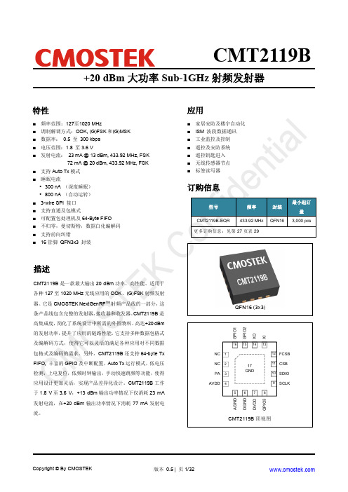
+20 dBm 大功率Sub-1GHz 射频发射器特性 ⏹ ⏹ ⏹ ⏹ ⏹ ⏹ ⏹ ⏹ ⏹ ⏹ ⏹ ⏹ ⏹ 应用于QFN16 (3X 3)17GNDCSB FCSB X IX OG P I O 2G P I O 1NC NC 13141516121112目录1.电气特性 (4)1.1推荐运行条件 (4)1.2绝对最大额定值 (4)1.3功耗 (5)1.4发射机 (5)1.5稳定时间 (6)1.6频率综合器 (6)1.7低电压检测 (6)1.8晶体 (7)1.9低频振荡器 (7)1.10数字接口 (7)1.11典型参数图表 (8)2.管脚描述 (10)3.典型应用原理图 (11)4.功能描述 (12)4.1发射器 (12)4.2辅助模块 (12)4.2.1晶体振荡器 (12)4.2.2睡眠计时器 (13)4.2.3低电压检测 (13)4.2.4快速手动跳频 (13)5.芯片运行 (14)5.1SPI接口 (14)5.2FIFO (14)5.2.1FIFO 读操作 (14)5.2.2FIFO 写操作 (15)5.2.3FIFO 相关中断 (15)5.3工作状态,时序及功耗 (16)5.3.1启动时序 (16)5.3.2工作状态 (16)5.4GPIO和中断 (18)6.数据包及包处理机 (20)6.1数据包格式 (20)6.2数据模式 (20)6.2.1直通模式 (21)6.2.2包模式 (21)7.自动运行模式 (22)8.用户寄存器 (23)8.1CMT区 (23)8.2系统区 (24)8.3频率区 (24)8.4数据率区 (24)8.5基带区 (25)8.6发射区 (25)8.7控制1区 (25)8.8控制2区 (26)9.订购信息 (27)10.封装信息 (28)11.顶部丝印 (29)11.1CMT2119B顶部丝印 (29)12.其它文档 (30)13.文档变更记录 (31)14.联系信息 (32)1. 电气特性V DD = 3.3 V,T OP = 25 °C,F RF = 433.92 MHz。
pt8211典型程序

pt8211典型程序1.引言1.1 概述概述部分是对整篇文章进行介绍和概括的部分。
在写概述部分时,应该简要介绍主题,突出重点,能够引起读者的兴趣。
对于文章《pt8211典型程序》的概述部分,可以写成以下内容:概述:本文将介绍pt8211,一个常用的音频解码器的典型程序。
pt8211是一种用于音频解码的芯片,它具有高性能和低功耗的特点,广泛应用于嵌入式系统、手机、音频设备等领域。
文章将从引言、正文和结论三个方面进行介绍。
引言部分将概述文章的整体结构和目的,为读者提供了解文章内容的框架。
正文部分将详细介绍pt8211的特点、工作原理以及实现典型程序的步骤。
通过具体的代码示例,读者将能够深入了解pt8211的使用方法和技巧。
结论部分将对整篇文章进行总结,并展望pt8211典型程序的发展前景。
本文的目的是为读者提供一个全面了解pt8211的平台,帮助读者更好地理解和应用pt8211解码器。
通过学习本文,读者将能够掌握pt8211的基本原理和常用的典型程序实现方法,为自己的项目提供有力的支持。
接下来,我们将在第二部分中详细介绍pt8211的特点和典型程序实现。
希望读者通过本文的学习,能够对pt8211有更深入的了解,提高自己在音频解码领域的技能水平。
1.2 文章结构文章结构:本文分为引言、正文和结论三个部分。
引言部分包括概述、文章结构和目的三个小节。
在概述中,将介绍pt8211这一主题的背景和重要性,引起读者的兴趣。
文章结构部分将说明本文的整体架构和各个章节的安排,使读者能够清晰地把握全文的脉络。
目的部分将说明本文的写作目的,即通过介绍pt8211典型程序的实现来帮助读者更好地理解和应用该技术。
正文部分主要包括pt8211的介绍和典型程序实现两个小节。
在pt8211的介绍中,将详细介绍pt8211这一技术的基本原理、特点和应用领域,帮助读者对pt8211有一个全面的了解。
在典型程序实现部分,将以实例的方式,逐步介绍pt8211的典型程序设计和实现方法,包括代码示例和详细的解析。
MAXIM MAX8211 MAX8212 说明书
________________General DescriptionMaxim’s MAX8211 and MAX8212 are CMOS micropower voltage detectors that warn microprocessors (µPs) of power failures. Each contains a comparator, a 1.5V bandgap reference, and an open-drain N-channel output driver. Two external resistors are used in conjunction with the internal reference to set the trip voltage to the desired level. A hysteresis output is also included, allowing the user to apply positive feedback for noise-free output switching.The MAX8211 provides a 7mA current-limited output sink whenever the voltage applied to the threshold pin is less than the 1.5V internal reference. In the MAX8212, a voltage greater than 1.5V at the threshold pin turns the output stage on (no current limit).The CMOS MAX8211/MAX8212 are plug-in replacements for the bipolar ICL8211/ICL8212 in applications where the maximum supply voltage is less than 16.5V. They offer sev-eral performance advantages, including reduced supply current, a more tightly controlled bandgap reference, and more available current from the hysteresis output.________________________ApplicationsµP Voltage Monitoring Undervoltage Detection Overvoltage Detection Battery-Backup Switching Power-Supply Fault Monitoring Low-Battery Detection____________________________Featureso µP Power-Fail Warningo Improved 2nd Source for ICL8211/ICL8212o Low-Power CMOS Design o 5µA Quiescent Currento On-Board Hysteresis Output o ±40mV Threshold Accuracy (±3.5%)o 2.0V to 16.5V Supply-Voltage Range o Define Output Current Limit (MAX8211)o High Output Current Capability (MAX8212)_______________Ordering InformationMAX8211/MAX8212Microprocessor Voltage Monitors with Programmable Voltage Detection________________________________________________________________Maxim Integrated Products 1___________________Pin Configuration___________Typical Operating Circuit19-0539; Rev 4; 9/02Ordering Information continued on last page.*Contact factory for dice specifications.For pricing, delivery, and ordering information,please contact Maxim/Dallas Direct!at 1-888-629-4642, or visit Maxim’s website at .M A X 8211/M A X 8212Microprocessor Voltage Monitorswith Programmable Voltage Detection 2_______________________________________________________________________________________Supply Voltage.......................................................-0.5V to +18V Output Voltage.......................................................-0.5V to +18V Hysteresis...................+0.5V to -18V with respect to (V+ + 0.5V)Threshold Input Voltage...............................-0.5V to (V+ + 0.5V)Current into Any Terminal.................................................±50mA Continuous Power Dissipation (T A = +70°C)8-Pin Plastic DIP (derate 9.09mW/°C above +70°C).....727mW 8-Pin SO (derate 5.88mW/°C above +70°C)..................471mW8-Pin CERDIP (derate 8.00mW/°C above +70°C)..........640mW 8-Pin TO-99 (derate 6.67mW/°C above +70°C).............533mW Operating Temperature RangesMAX821_C_ _.......................................................0°C to +70°C MAX821_E_ _.....................................................-40°C to +85°C MAX821_M_ _..................................................-55°C to +125°C Storage Temperature Range.............................-65°C to +150°C Lead Temperature (soldering, 10s).................................+300°CStresses beyond those listed under “Absolute Maximum Ratings” may cause permanent damage to the device. These are stress ratings only, and functional operation of the device at these or any other conditions beyond those indicated in the operational sections of the specifications is not implied. Exposure to absolute maximum rating conditions for extended periods may affect device reliability.ABSOLUTE MAXIMUM RATINGSELECTRICAL CHARACTERISTICS(V+ = 5V, T= +25°C, unless otherwise noted.)MAX8211/MAX8212Microprocessor Voltage Monitors with Programmable Voltage Detection________________________________________________________________________________________3Note 1:The maximum output current of the MAX8211 is limited by design to 30mA under any operating condition. The output voltagemay be sustained at any voltage up to +16.5V as long as the maximum power dissipation of the device is not exceeded.Note 2:The maximum output current of the MAX8212 is not defined, and systems using the MAX8212 must therefore ensure that theoutput current does not exceed 50mA and that the maximum power dissipation of the device is not exceeded.ELECTRICAL CHARACTERISTICS (continued)(V+ = 5V, T A = +25°C, unless otherwise noted.)PARAMETER SYMBOL CONDITIONSUNITSI OUT = 2mA, V TH = 1.0V 0.170.4Output Saturation Voltage V OL I OUT = 2mA, V TH = 1.3V 0.170.4V V TH = 1.0V (Note 1)47.0Maximum Available Output CurrentI OHC temp. range,V OUT = 5VV TH = 1.3V (Note 2)1235mAT A = TMIN to T MAX , C/E temp. ranges, V+ = 16.5V, V TH = 1.0V,V HYST = -16.5V with respect to V+0.10.1Hysteresis Leakage CurrentI LHYST A = T MIN to T MAX , M temp. range, V+ = 16.5V, V TH = 0.9V,V HYST = -16.5V with respect to V+33µAHysteresis Saturation VoltageV HYS (MAX)I HYST = 0.5mA, V TH = 1.3V,measured with respect to V+-0.1-0.2-0.1-0.2V Maximum Available Hysteresis CurrentV HYS (MAX)V TH = 1.3V, V HYS = 0V210210mAMAX8212MIN TYP MAXMAX8211MIN TYP MAX _______________Detailed DescriptionAs shown in the block diagrams of Figures 1 and 2, the MAX8211 and MAX8212 each contain a 1.15V refer-ence, a comparator, an open-drain N-channel output transistor, and an open-drain P-channel hysteresis out-put. The MAX8211 output N-channel turns on when the voltage applied to the THRESH pin is less than the internal reference (1.15V). The sink current is limited to 7mA (typical), allowing direct drive of an LED without a series resistor. The MAX8212 output turns on when the voltage applied to THRESH is greater than the internal reference. It is not current limited, and will typically sink 35mA.Compatibility with ICL8211/ICL8212The CMOS MAX8211/MAX8212 are plug-in replacements for the bipolar I CL8211/I CL8212 in most applications.The use of CMOS technology has several advantages.The quiescent supply current is much less than in the bipolar parts. Higher-value resistors can also be usedFigure 1. MAX8211 Block DiagramM A X 8211/M A X 8212Microprocessor Voltage Monitorswith Programmable Voltage Detection 4_______________________________________________________________________________________Figure 3. Basic Overvoltage/Undervoltage Circuitin the networks that set up the trip voltage, since the comparator input (THRESH pin) is a low-leakage MOSFET transistor. This further reduces system current drain. The tolerance of the internal reference has also been significantly improved, allowing for more precise voltage detection without the use of potentiometers.The available current from the HYST output has been increased from 21µA to 10mA, making the hysteresis feature easier to use. The disparity between the HYST output and the voltage required at THRESH to switch the OUT pin has also been reduced in the MAX8211from 8mV to 0.1mV to eliminate output “chatter” or oscillation.Most voltage detection circuits operate with supplies of 15V or less; in these applications, the MAX8211/MAX8212 will replace I CL8211/I CL8212s with the per-formance advantages described above. However, note that the CMOS parts have an absolute maximum sup-ply-voltage rating of 18V, and should never be used in applications where this rating could be exceeded.Exercise caution when replacing I CL8211/ICL8212s in closed-loop applications such as programmable zeners. Although neither the I CL8211/I CL8212 nor the MAX8211/MAX8212 are internally compensated, the CMOS parts have higher gain and may not be stable for the external compensation-capacitor values used in lower-gain ICL8211/ICL8212 circuits.__________Applications InformationBasic Voltage DetectorsFigure 3 shows the basic circuit for both undervoltage detection (MAX8211) and overvoltage detection (MAX8212). For applications where no hysteresis is needed, R3 should be omitted. The ratio of R1 to R2 is then chosen such that, for the desired trip voltage at V IN ,1.15V is applied to the THRESH pin. Since the com-parator inputs are very low-leakage MOSFET transis-tors, the MAX8211/MAX8212 can use much higherresistors values in the attenuator network than can the bipolar I CL8211/I CL8212. See Table 1 for switching delays.Table 1. Switching DelaysVoltage Detectors with HysteresisTo ensure noise-free output switching, hysteresis is frequently used in voltage detectors. For both the MAX8211 and MAX8212 the HYST output is on for threshold voltages greater than 1.15V. R3 (Figure 3)controls the amount of current (positive feedback) sup-plied from the HYST output to the mid-point of the resis-tor divider, and hence the magnitude of the hysteresis,or dead-band.Figure 2. MAX8212 Block DiagramCalculate resistor values for Figure 3 as follows:1)Choose a value for R1. Typical values are in the 10k Ω to 10M Ω range.2)Calculate R2for the desired upper trip point Vusing the formula:3)Calculate R3 for the desired amount of +Figure 5 shows an alternate circuit, suitable only when thevoltage being detected is also the power-supply voltage for the MAX8211 or MAX8212.Calculate resistor values for Figure 5 as follows:1)Choose a value for R1. Typical values are in the 10k Ω to 10M Ω range.2)Calculate R2:3)Calculate R3:Low-Voltage Detector for Logic SupplyThe circuit of Figure 5 will detect when a 5.0V (nominal)supply goes below 4.5V, which is the V MIN normally specified in logic systems. The selected resistor values ensure that false undervoltage alarms will not be gener-ated, even with worst-case threshold trip values and resistor tolerances. R3 provides approximately 75mV of hysteresis.MAX8211/MAX8212Microprocessor Voltage Monitors with Programmable Voltage Detection________________________________________________________________________________________5Figure 4. MAX8211/MAX8212 Threshold Trip Voltage vs.Ambient TemperatureFigure 5. MAX8211 Logic-Supply Low-Voltage DetectorM A X 8211/M A X 8212Microprocessor Voltage Monitorswith Programmable Voltage Detection 6________________________________________________________________________________________Ordering Information (continued)_____________________________________________Pin Configurations (continued)*Contact factory for dice specifications.MAX8211/MAX8212Microprocessor Voltage Monitors with Programmable Voltage Detection_______________________________________________________________________________________7Package Information(The package drawing(s) in this data sheet may not reflect the most current specifications. For the latest package outline information,go to /packages .)M A X 8211/M A X 8212Microprocessor Voltage Monitorswith Programmable Voltage Detection 8_______________________________________________________________________________________Package Information (continued)(The package drawing(s) in this data sheet may not reflect the most current specifications. For the latest package outline information,go to /packages .)MAX8211/MAX8212Microprocessor Voltage Monitors with Programmable Voltage Detection_______________________________________________________________________________________9Package Information (continued)(The package drawing(s) in this data sheet may not reflect the most current specifications. For the latest package outline information,go to /packages .)Ma xim ca nnot a ssume responsibility for use of a ny circuitry other tha n circuitry entirely embodied in a Ma xim product. No circuit pa tent licenses a re implied. Maxim reserves the right to change the circuitry and specifications without notice at any time.10__________________Maxim Integrated Products, 120 San Gabriel Drive, Sunnyvale, CA 94086 (408) 737-7600©2002 Maxim Integrated ProductsPrinted USAis a registered trademark of Maxim Integrated Products.M A X 8211/M A X 8212Microprocessor Voltage Monitorswith Programmable Voltage DetectionPackage Information (continued)(The package drawing(s) in this data sheet may not reflect the most current specifications. For the latest package outline information,。
ITECH IT8211 说明书

版权归属于艾德克斯电子(南京)有限公司Ver3.0/Jan, 2010/ IT8211用户使用手册直流电子负载 型号 IT8211广州伊测推荐--艾德克斯经济型电子负载IT8211 150W 60V 30A 华南销售电话:020-81097620安全规则为防止触电,非本公司授权人员,严禁拆开机器。
严禁将本设备使用于生命维持系统或其他任何有安全要求的设备上。
我们对于使用本产品时可能发生的直接或间接财务损失,不承担责任。
认证与品质保证艾德克斯电子保证本产品性能于工厂交 付时,符合本手册所标称的各项技标。
WARNINGSafety RegulationsCertificationNoticeTo avoid electrical shock, do not open the cabinet. Refer servicing to qualified personnel only.To avoid injuries, always disconnect power, discharge circuits, and remove external voltage sources before touching components. KEEP AWAY FROM LIVE CIRCUITS.We cannot accept responsibility for any direct or indirect financial damage or loss of profit that might occur when using the power supply.The instrument chassis and cover must be connected to an electrical ground.We certify that this product met its published specifications at time of shipment from the factory.T h e inf orm a t io n c o n ta in e d i n th i s document is subjectto changewithout notice.通告本手册的内容如有更改,恕不另行通知。
AT11V 无线门铃芯片

AT11VAT11V学习码门铃芯片描述:目前市场上的门铃大多采用2262编码加2272解码的方案,此方案存在编码量少极易重码,体积大,要手动跳线不易生产等缺点。
为改善以上缺点超通和龙公司专门开发出AT11V学习码门铃芯片,此芯片方案适用于无线遥控门铃产品。
特点:编码芯片采用MT361/TDH1100学习码芯片,特点如下:外部元器件少工作电压:1.8~13.5V(采用《TDH1100应用电路》的接法可以直接用12V电池供电)100万组编码自动延时发射功能(可选)解码芯片采用AT11V芯片,特点如下:标准可学习存储4个遥控器容错能力强自动波特率调整可控制高频接收模块间歇供电,大大降低接收模块功耗可支持两通道输出典型应用无线遥控门铃脚位图:AT11VMT361/MT361/TDH1100TDH1100管脚说明:AT11V 管脚说明:TDH1100极限参数:名称管脚说明VDD1电源正NC 2空脚NC3空脚DEC14功能检测脚1DOUT 5数据输出LED 6LED指示灯输出DEC27功能检测脚2VSS8电源负名称管脚说明VDD 1电源正SCL/STUDY 2外接存储器时钟/学习按键脚SDA 3外接存储器数据脚RFIN 4高频信号输入脚OUT15音频信号1输出脚OUT26音频信号2输出脚(此功能可选)RFPOWER 7高频电源控制脚VSS8电源负符号参数参数范围单位Vcc 电源电压-0.3~13.5V VI 输入电压-0.3~Vcc +0.3V VO 输出电压-0.3~Vcc +0.3V Tst 存储温度-40~125℃Top 工作温度-20~70℃Pdis最大功耗150mWAT11VMT361/MT361/TDH1100TDH1100电气参数:AT11V 极限参数:AT11V 电气参数:符号参数测试条件最小值典型值最大值单位Vcc 电源电压 1.80-12.00V Isb静态电流VCC=12V振荡器停振K0,K1开路1uAIop 工作电流VCC=5V OSC =80KHZ 0.51mA Ioh 输出驱动电流VCC=5V,Voh=2.5V -3mA Iol输出陷电流VCC=5V,Voh=2.5V3mA符号参数参数范围单位Vcc 电源电压-0.3~6.0V VI 输入电压-0.3~Vcc +0.3V VO 输出电压-0.3~Vcc +0.3V Tst 存储温度-40~125℃Top 工作温度0~70℃Pdis最大功耗150mW符号参数测试条件最小值典型值最大值单位Vcc 电源电压 2.0- 5.5V Icc平均工作电流VCC=4.5V0.12mAAT11VAT11V 学习码门铃芯片方案与2262/2272门铃方案对比表:序号比对项目AT11V 学习码2262/2272固定码1编码地址1048576组6561组2发射芯片编码方式出厂时已自动设定好要手动跳线3对码方式学习型,只要发射机与接收机无线对码即可使用接收端要手动跳线,且要与发射机跳线一致才可使用,不易生产且容易出错4如要新增遥控器直接无线对码,无需拆开遥控器和接收机手动跳线对码,要拆开遥控器和接收机5高频接收模块电源可以控制高频接收模块间歇供电,大大降低接收模块功耗不可控制高频接收模块电源6发射与接收振荡电阻匹配接收机采用自动波特率调整接收,接收机无需外接振荡电阻,更不需要与发射机匹配接收机的振荡电阻与发射机的振荡电阻要按要求配对才能使用7封装脚数发射芯片:8脚接收芯片:8脚发射芯片:18脚或20脚接收芯片:18脚或20脚封装信息1封装标识信息8引脚SOIC(150mil)示例AT11V 2封装详细信息。
IKEA RTA-8211 文档说明书
P.6
STEP 1 Hardware:
L 6x25mm x4
Scan QR Code to view this step
RTA-8211
STEPS FOR ASSEMBLY
2 1
3
P.6
5 2
1
3
STEP 2
Hardware:
4X35mm
C
x4
4X20mm
D
x2
Scan QR Code to view this step
RTA-8211
STEPS FOR ASSEMBLY
4
9
10
9 4
P.8
10
4
4
Scan QR Code to view this step
IMPORTANT: Make sure you use in this step the correct sliders ( 4 ) which are longer and have more holes than sliders ( 22 ). Use screws ( B ) to assemble the scanner sliders ( 4 ) to the top sets of slider holes on panels ( 9 ) and ( 10 ) in the following order: First open the slider slowly until the first hole on the front of the slider is visible through the big opening, and attach to the front hole on the panels as shown. The open the slider completely and attach to the 2 back holes as shown.
微昂 ME6214 低功耗低压差大电流线性稳压器说明书
ME62140.7uA 超低功耗、低压差大电流线性稳压器概述ME6214系列是以 CMOS 工艺制造的超低静态功耗、低压差线性稳压器。
稳压器消耗电流约0.7uA ,使能关断后功耗为0.01uA (典型)。
内置使能控制,限流电路以及折返短路保护,并有使能控制输出电容自动放电功能。
特点 ● 超低功耗:工作时:0.7uA (典型) 休眠时:0.01uA (典型) ● 输入电压范围:2.0~18V● 输出电压范围:1.5~5.0V (间隔0.1V ) ● 输出精度:±2%● 输入输出电压差:160mV@ I OUT =100mA (3.3V ) ● 输出电流:300mA● 电流保护: 折返短路电流30mA过流保护● 使能控制:高电平ON/低电平OFF ,不能悬空 输出电容自动放电功能 ME6214C 系列为带使能版本 ME6214A 系列为不带使能版本 应用场合 封装形式● 以电池供电的设备的稳压电源 ● 3-pin SOT89-3,SOT23-3 ● 家电产品的稳压电源 ● 5-pin SOT23-5 ● 携带通信设备、数码相机、数码音响设备的稳压电源 ● 6-pin DFN2X2-6L典型应用图VoutNCCE VSSVIN CIN1uFCIN 1uFME6214选购指南1. 产品型号说明ME 62 14X XX XG环保标识封装形式M3-SOT23-3 M5-SOT23-5版本或功能产品品种产品类别公司标识输出电压如:A-无使能 C-有使能P-SOT89-3 N6-DFN2*2-6L目前产品的电压值共有5种:1.5V 、1.8V 、2.8V 、3.0V 、3.3V 、4.5V 、5.0V 。
如需其他电压值或封装形式,请联系我司销售人员。
产品脚位图VSS VOUTVINVSS VIN VOUT VIN VSS CESOT23-3 SOT89-3 SOT23-5 DFN2*2-6L 脚位功能说明ME6214AXX功能框图OUTVSSVIN模块功能示意图绝对最大额定值注意:绝对最大额定值是本产品能够承受的最大物理伤害极限值,请在任何情况下勿超出该额定值。
长虹彩电常见故障及维修大全
长虹彩电常见故障及维修大全(一)长虹11、在检修a6机芯生产的21"彩电故障时,或检修因tda7496损坏无伴音故障时,将crt、主声道左右喇叭网和主板地用屏敝线相连。
2、针对个别型号的彩电在信号较差的地区接收信号出现雪花点较多,且出现有噪音出现的问题,可采取在前置中频放大电路v101"e"极电阻r115两端并接一只电容解决,参考值为0.01uf。
3、a6机芯生产的各型彩电当出现黑白图象显示正常,色饱和度开大后,满屏绿色画面的故障,主要检查la7688(1)脚外电路上的元件和基带延迟处理块lc89950。
判定方法是:测量la7688(1)脚电压,当电视机接收tv-pal/ntsc制时,该脚工作电压应设置在1.7-2.6v 间。
当电视机工作av-pal/ntsc制时,此脚应为2.9-3.8v。
当(1)脚电压正常,则故障在lc89950及周围电路上。
4、a6机芯生产的21〃彩电出现节目号"1"下的节目关机后频率漂移现象,而在其它节目号下无此现象,解决方法是将原装cpu换成cht0408-5l21。
cht0408-5l21可代替cht0405-5j77、ch0403-5h61。
5、la7688a可用la7688b代替。
为避免多次损坏la7688a,可在印制板号为ju7.820.1534/1360的y板上在r362左端与vd622正端之间背焊一只电容。
在板号为:ju7.820.1535/1462的y 板上在v617"c"极与显象管座接地脚间背焊一只电容。
该电容大小为:ct-500v-100p。
长虹26、cn-5机芯出现开机有图,随后出现水平亮线故障,请检查an5095(20)脚外接自动亮度控制电路上的元件,该脚电压低于0.7v时,(20)脚内接维修开关电路启动引起。
7、cn-5开关电源所用元件必须用本机规定的型号,如开关管必须用thd215。
功放集成芯片
•
最新标准虚拟杜比环绕声芯片 QS7779/QS7785
• QS7779/QS7785是加拿大Qsound音频实验室推出的单片虚拟化环绕 音效处理电路,是目前业界公认的处理效果最接近自然原声的虚拟杜 比环绕芯片!QS7779为2入2出方式,QS7785为2入5出,两者内部 都包括了杜比定向逻辑和DVD(AC-3)混合信号解码器,使用Qsound 实验室的专利Qsurround虚拟环绕技术,并由Qsound实验室授权使用, 该芯片的主要功能是:(1)如果输入的是普通的立体声信号,则进 行立体声效果增强:(2)如果输入的是2声道的矩阵编码信号(杜比 定向逻辑或混合AC-3信号)则先将其解码,再虚拟化合成2声道或5 声道输出。 QS7779主要特点: 1.内带杜比定向逻辑和 DVD(AC-3) 混合信号解码输器,使用2只扬声器实现虚拟化环绕声。 2.信噪比 11db, 动态范围110db . QS7785主要特点: 1.内带杜比定向逻辑和 DVD(AC-3)混合信号解码输器,解出的环绕信号为2声道全频带,和 AC-3环绕声相同,优于杜比定向逻辑系统。 2.前方采用3 D立体声增 强技术,后方采用3D合成虚拟环绕技术,分两种增强方式(低增强和 高增强),具有中置输出及低音增强功能。 3.使用5声道实现环绕声, 也可用2声道输出方式。 4..信噪比11db, 动态范围110db
• TDA7294
LM4610N
• LM4610是美国国家半导体公司的高品质直流控制音响电路。 它是一块利用直流电压控制音调、音量和声道平衡的立体声集 成电路,并且具有3D音场处理、等响度补偿功能。该电路控制 平滑流畅,音质自然流畅,高频清晰、解析力佳,其产生的3D 环绕声场具有很强的三维空间感和包围感,主观感觉与SRS的 效果类似。 LM4610N的主要电气参数如下:具有3 D声场处理 功能和响度补偿功能。响度补偿是针对人耳在音量较小时对高 低频信号的灵敏度下降,因而在不同音量时对高、低频端作适 度的提升补偿,使人耳在任何响度下始终听到平坦、均衡的响 应。它的电压范围是:9V~16V(典型为12伏,电流为35毫安); 失真度仅0.03%;信嘈比高达80dB;频宽达250 kHz,音量调节 为75dB;平衡调节为1~20dB;音调调节范围为±15dB;最大增 益2dB;LM4610N具有输入阻抗高(30Ω),输出电阻低(2 0Ω)的优点。用LM6410N音调控制电路对提高音质和加强低 频力度及三维空间感作用突出。可以说LM4610N是组装功放系 统或替换调音部分的精品。
- 1、下载文档前请自行甄别文档内容的完整性,平台不提供额外的编辑、内容补充、找答案等附加服务。
- 2、"仅部分预览"的文档,不可在线预览部分如存在完整性等问题,可反馈申请退款(可完整预览的文档不适用该条件!)。
- 3、如文档侵犯您的权益,请联系客服反馈,我们会尽快为您处理(人工客服工作时间:9:00-18:30)。
TOSHIBA Bipolar Linear Integrated Circuit Silicon MonolithicTA8211AHDual Audio Power AmplifierThe TA8211AH is dual audio power amplifier for consumerapplications.This IC provides an output power of 6 watts per channel (at V CC = 20 V, f = 1 kHz, THD = 10%, R L = 8 Ω).It is suitable for power amplifier of TV and home stereo.Features· High output power: P out = 6 W/channel (Typ.)(V CC = 20 V, R L = 8 Ω, f = 1 kHz, THD = 10%)· Low noise: V no = 0.14 mVrms (Typ.)(V CC = 28 V, R L = 8 Ω, G V = 34dB, R g = 10 kΩ,BW = 20 Hz~20 kHz)· Very few external parts· Built in thermal shut down protector circuit· Operating supply voltage range: V CC (opr) = 10~30 V (Ta = 25°C)Block DiagramWeight: 4.04 g (typ.)V CCApplication InformationVoltage gainThe closed loop voltage gain is determined by R 1, R 2.~ - 34(dB)(a)Amplifier with gain > 34dBWhen R 3 = 400 W G V ~ - 40 (dB) is given.(b)Amplifier with gain < 34dBWhen R 4 = 220 W G V ~ - 30 (dB) is given.CautionsThis IC is not proof enough against a strong E-M field by CRT which may cause malfunction such as leak. Please set the IC keeping the distance from CRT.WW+W = 400 400k 20og20l (dB)R R R og20G 221V +=l (dB)//R R //R R R og 20G 32321V +=l (dB)R R R R R og20G 42421V +++=lFigure 2Figure 3Standard PCB(Bottom view)Maximum Ratings (Ta = 25°C)Characteristics Symbol Rating UnitSupply voltageV CC 30 V Output current (Peak/ch) I O (peak) 2 A Power dissipation P D (Note) 25WOperating temperature T opr -20~75 °C Storage temperatureT stg-55~150 °CNote: Derated above Ta = 25°C in the proportion of 200 mW/°C.Electrical Characteristics(unless otherwise specified, V CC = 20 V, R L = 600 9, R g = 600 9, f = 1 kHz, Ta = 25°C)Characteristics SymbolTestCircuitTest ConditionMinTyp.MaxUnit Quiescent current I CCQ ¾V in = 0¾ 75 130mA P out (1) ¾ THD = 10% 5.06.0¾Output powerP out (2) ¾ THD = 1% ¾ 4.5 ¾WTotal harmonic distortion THD ¾ P out = 2 W¾ 0.1 0.6 % Closed loop voltage gain G V ¾ V out = 0.775 Vrms (0dBm) 32.5 34.0 35.5dBOpen loop voltage gain G VO ¾¾ 60 ¾ dB Input resistance R IN ¾ ¾¾ 30 ¾ k WRipple rejection ratio R.R. ¾ Rg = 0, f ripple = 100 HzV ripple = 0.775 Vrms (0dBm) -45-57¾ dBOutput noise voltageV no¾Rg = 10 k W ,BW = 20 Hz~20 kHz¾ 0.14 0.3 mVrmsTyp. DC Voltage of Each Terminal (V CC = 20 V, Ta = 25°C)Terminal No. 1 2 3 4 5 6 7 8 9 10 11 12 DC voltage (V)2.12.25GND2.252.16.89.82.25V CC GND 2.259.8Test CircuitV CC INPUT1INPUT20.030.1 0.3 1 10 303 0 8 16 24 32 40T o t a l h a r m o n i c d i s t o r t i o n T H D (%)T o t a l h a r m o n i c d i s t o r t i o n T H D (%)O u t p u t D C v o l t a g e V O U T (D C ) (V )Supply voltage V CC (V)I CCQ , V OUT (DC) – V CCQ u i e s c e n t c u r r e n t I C C Q (m A )Frequency f (Hz)G V– fV o l t a g e g a i n G V (d B )Output power P out (W)T o t a l h a r m o n i c d i s t o r t i o n T H D (%)Output power P out (W)THD – P outFrequency f (Hz) THD – fFrequency f (Hz)C.T. – fC r o s s t a l k C .T . (d B )--------301003001k 3k 10k 30k 100k0.3 1 3 10 100 3003030 -----100 300 1k --3k 10k 30k 100k --2040 60 80-402040 60 8030-----100 300 1k --3k 10k 30k 100k ---30----1003001k --3k 10k 30k---O u t p u t n o i s e v o l t a g e V n o (m V r m s )O u t p u t n o i s e v o l t a g e V n o (m V r m s )Signal source resistance Rg (W ) C.T. – RgC r o s s t a l k C .T . (d B )Frequency f (Hz)R.R. – fR i p p l e r e j e c t i o n r a t i o R .R . (d B )Signal source resistance Rg (W )R.R. – RgR i p p l e r e j e c t i o n r a t i o R .R . (d B )Signal source resistance Rg (W )V no – RgAmbient temperature Ta (°C)V no – TaAmbient temperature Ta (°C)I CCQ – TaQ u i e s c e n t c u r r e n t I C C Q (m A )301003001k 3k 10k 30k 100k25 50 100 17575125 150 04 8 12 16 201014 18 22 26 30-2040 60 808 1624 32 40A l l o w a b l e p o w e r d i s s i p a t i o n P D (W )P o w e r d i s s i p a t i o n P D (W )Ambient temperature Ta (ºC)THD – TaT o t a l h a r m o n i c d i s t o r a t i o n T H D (%)Supply voltage V CC (V)P out – V CCO u t p u t p o w e r P o u t (W )Supply voltage V CC (V)P D MAX – V CCM a x i m u m p o w e r d i s s i p a t i o n P D M A X (W )Output power P out (W)P D – P outAmbient temperature Ta (°C)P D – TaPackage DimensionsWeight: 4.04 g (typ.)· TOSHIBA is continually working to improve the quality and reliability of its products. Nevertheless, semiconductor devices in general can malfunction or fail due to their inherent electrical sensitivity and vulnerability to physical stress. It is the responsibility of the buyer, when utilizing TOSHIBA products, to comply with the standards of safety in making a safe design for the entire system, and to avoid situations in which a malfunction or failure of such TOSHIBA products could cause loss of human life, bodily injury or damage to property.In developing your designs, please ensure that TOSHIBA products are used within specified operating ranges as set forth in the most recent TOSHIBA products specifications. Also, please keep in mind the precautions and conditions set forth in the “Handling Guide for Semiconductor Devices,” or “TOSHIBA Semiconductor Reliability Handbook” etc.. · The TOSHIBA products listed in this document are intended for usage in general electronics applications (computer, personal equipment, office equipment, measuring equipment, industrial robotics, domestic appliances, etc.). These TOSHIBA products are neither intended nor warranted for usage in equipment that requires extraordinarily high quality and/or reliability or a malfunction or failure of which may cause loss of human life or bodily injury (“Unintended Usage”). Unintended Usage include atomic energy control instruments, airplane or spaceship instruments, transportation instruments, traffic signal instruments, combustion control instruments, medical instruments, all types of safety devices, etc.. Unintended Usage of TOSHIBA products listed in this document shall be made at the customer’s own risk. · This product generates heat during normal operation. However, substandard performance or malfunction may cause the product and its peripherals to reach abnormally high temperatures.The product is often the final stage (the external output stage) of a circuit. Substandard performance or malfunction of the destination device to which the circuit supplies output may cause damage to the circuit or to the product. · The products described in this document are subject to the foreign exchange and foreign trade laws.· The information contained herein is presented only as a guide for the applications of our products. No responsibility is assumed by TOSHIBA CORPORATION for any infringements of intellectual property or other rights of the third parties which may result from its use. No license is granted by implication or otherwise under any intellectual property or other rights of TOSHIBA CORPORATION or others. · The information contained herein is subject to change without notice.000707EBFRESTRICTIONS ON PRODUCT USE。