IC datasheet pdf-OPA2333-Q1,pdf(1.8-V Micropower CMOS Operational Amplifier Zero-Drift Series)
IC datasheet pdf-REF1004,pdf(Micropower Voltage Reference)

The REF1004 is offered in an 8-lead Plastic SOIC package and shipped in anti-static rails or tape and reel.
Typical Operating Circuit
NC 1 NC 2 NC 3 Anode 4
IR = 100µA
10Hz ≤ IR ≤ 10kHz
60
120
µV
LONG TERM STABILITY
IR = 100µA
TA = 25°C ± 0.1°C
20
2 (1) This specification applies over the full operating temperature range of 0°C ≤ TA ≤ 70°C. (2) This specification applies over the full operating temperature range of 40°C ≤ TA ≤ +85°C. (3) Denotes the specifications which apply over the full operating temperature range.
OPA2333SHKJ,OPA2333SJD,OPA2333SKGD1, 规格书,Datasheet 资料
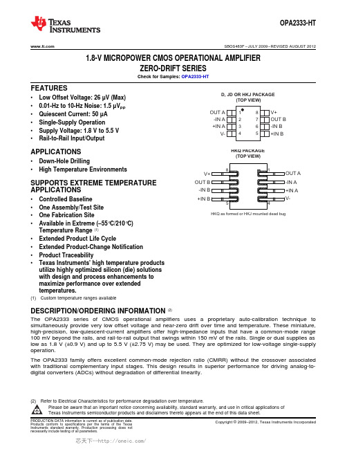
HKQ PACKAGE(TOP VIEW)8541HKQ as formed or HKJ mounted dead bugOUT A-IN A+IN AV-+IN B-IN BOUT BV+D, JD OR HKJ PACKAGEOUT-IN+INBOPA2333-HT SBOS483F–JULY2009–REVISED AUGUST20121.8-V MICROPOWER CMOS OPERATIONAL AMPLIFIERZERO-DRIFT SERIESCheck for Samples:OPA2333-HTFEATURES•Low Offset Voltage:26μV(Max)•0.01-Hz to10-Hz Noise:1.5μV PP•Quiescent Current:50μA•Single-Supply Operation•Supply Voltage:1.8V to5.5V•Rail-to-Rail Input/OutputAPPLICATIONS•Down-Hole Drilling•High Temperature EnvironmentsSUPPORTS EXTREME TEMPERATUREAPPLICATIONS•Controlled Baseline•One Assembly/Test Site•One Fabrication Site•Available in Extreme(–55°C/210°C)Temperature Range(1)•Extended Product Life Cycle•Extended Product-Change Notification•Product Traceability•Texas Instruments'high temperature productsutilize highly optimized silicon(die)solutionswith design and process enhancements tomaximize performance over extendedtemperatures.(1)Custom temperature ranges availableDESCRIPTION/ORDERING INFORMATION(2)The OPA2333series of CMOS operational amplifiers uses a proprietary auto-calibration technique to simultaneously provide very low offset voltage and near-zero drift over time and temperature.These miniature, high-precision,low-quiescent-current amplifiers offer high-impedance inputs that have a common-mode range 100mV beyond the rails,and rail-to-rail output that swings within150mV of the rails.Single or dual supplies as low as1.8V(±0.9V)and up to5.5V(±2.75V)may be used.They are optimized for low-voltage single-supply operation.The OPA2333family offers excellent common-mode rejection ratio(CMRR)without the crossover associated with traditional complementary input stages.This design results in superior performance for driving analog-to-digital converters(ADCs)without degradation of differential linearity.to Electrical Characteristics for performance degradation over temperature.Please be aware that an important notice concerning availability,standard warranty,and use in critical applications ofTexas Instruments semiconductor products and disclaimers thereto appears at the end of this data sheet.PRODUCTION DATA information is current as of publication date.Copyright©2009–2012,Texas Instruments Incorporated Products conform to specifications per the terms of the TexasInstruments standard warranty.Production processing does notnecessarily include testing of all parameters.OPA2333-HTSBOS483F–JULY2009–REVISED Table1.ORDERING INFORMATION(1)TA PACKAGE ORDERABLE PART NUMBER TOP-SIDE MARKINGKGD OPA2333SKGD1NAJD OPA2333SJD OPA2333SJD –55°C to210°CHKJ OPA2333SHKJ OPA2333SHKJHKQ OPA2333SHKQ OPA2333SHKQ –55°C to175°C D OPA2333HD O2333H(1)For the most current package and ordering information,see the Package Option Addendum at the end of this document,or see the TIWeb site at .BARE DIE INFORMATIONBACKSIDE BOND PAD DIE THICKNESS BACKSIDE FINISHPOTENTIAL METALLIZATION COMPOSITION 15mils.Silicon with backgrind V-Al-Si-Cu(0.5%)Table2.BOND PAD COORDINATESDESCRIPTION PAD NUMBER a b c d OUT A121.201288.5097.201364.50–IN A221.20923.6597.20999.65+IN A321.20533.0597.20609.05V–431.30172.20107.30248.20+IN B5864.80162.25940.80238.25–IN B6864.80552.65940.80628.65OUT B7864.80897.10940.80973.10V+8854.701280.45930.701356.452Submit Documentation Feedback Copyright©2009–2012,Texas Instruments IncorporatedProduct Folder Links:OPA2333-HT||||962mm 1490mm m||OPA2333-HTSBOS483F –JULY 2009–REVISED AUGUST 2012Copyright ©2009–2012,Texas Instruments IncorporatedSubmit Documentation Feedback3Product Folder Links:OPA2333-HTOPA2333-HTSBOS483F–JULY2009–REVISED THERMAL CHARACTERISTICS FOR JD PACKAGEover operating free-air temperature range(unless otherwise noted)PARAMETER TEST CONDITIONS MIN TYP MAX UNITHigh-K board(2),no airflow64.9Junction-to-ambient thermalθJA°C/W resistance(1)No airflow83.4θJB Junction-to-board thermal resistance High-K board without underfill27.9°C/WθJC Junction-to-case thermal resistance 6.49°C/W (1)The intent ofθJA specification is solely for a thermal performance comparison of one package to another in a standardized environment.This methodology is not meant to and will not predict the performance of a package in an application-specific environment.(2)JED51-7,high effective thermal conductivity test board for leaded surface mount packagesTHERMAL CHARACTERISTICS FOR HKJ OR HKQ PACKAGEover operating free-air temperature range(unless otherwise noted)PARAMETER MIN TYP MAX UNITto ceramic side of case 5.7θJC Junction-to-case thermal resistance°C/Wto top of case lid(metal side of case)13.7 THERMAL CHARACTERISTICS FOR D PACKAGEover operating free-air temperature range(unless otherwise noted)PARAMETER MIN TYP MAX UNITθJC Junction-to-case thermal resistance(to bottom of case)39.4°C/W Absolute Maximum Ratings(1)over operating free-air temperature range(unless otherwise noted)MIN MAX UNIT Supply voltage7V Signal input terminals,voltage(2)–0.3(V+)+0.3V Output short circuit(3)ContinuousJD,HKJ,HKQ packages–55210Operating temperature range°CD package–55175JD,HKJ,HKQ packages210Junction temperature°CD package175Human-Body Model(HBM)4000ESD rating VCharged-Device Model(CDM)1000(1)Stresses beyond those listed under"absolute maximum ratings"may cause permanent damage to the device.These are stress ratingsonly,and functional operation of the device at these or any other conditions beyond those indicated under"recommended operating conditions"is not implied.Exposure to absolute-maximum-rated conditions for extended periods may affect device reliability.(2)Input terminals are diode clamped to the power-supply rails.Input signals that can swing more than0.3V beyond the supply rails shouldbe current limited to10mA or less.(3)Short circuit to ground,one amplifier per package.4Submit Documentation Feedback Copyright©2009–2012,Texas Instruments IncorporatedProduct Folder Links:OPA2333-HTOPA2333-HT SBOS483F–JULY2009–REVISED AUGUST2012Electrical Characteristics:V S=1.8V to5.5VBoldface limits apply over the specified temperature range,T A=–55°C to210°C.At T A=25°C,R L=10kΩconnected toV S/2,V CM=V S/2,and V OUT=V S/2(unless otherwise noted).T A=–55°C to125°C T A=175°C(1)T A=210°C(2)UNIT PARAMETER TEST CONDITIONS MIN TYP MAX MIN TYP MAX MIN TYP MAXOFFSETVOLTAGEInput offsetV OS V S=5V210μV voltageover222626μV temperaturevsdV OS/d T0.020.050.05μV/°C temperaturevs powerPSRR V S=1.8V to5.5V16 1.28 1.711μV/V supplyLong-termSee(3)stability(3)Channel0.1μV/V separation,dcINPUT BIASCURRENTInput bias current I B±70±200pAover±150±1250±5300pA TemperatureInput offset±1060I OS±140±400±700pA current0NOISEInput voltagenoise,0.3 1.0 1.0μV PPf=0.01Hz to1HzInput voltagenoise,1.1 1.5 1.5μV PPf=0.1Hz to10HzInput currenti n100fA/√Hz noise,f=10HzINPUTVOLTAGERANGECommon mode(V–)–(V+)(V–)–(V–)+(V–)–(V–)+ V CM V voltage range0.1+0.10.250.250.250.25Common-ModeCMRR(V–)–0.1V<V CM<(V+)+0.1V10213010191dB Rejection RatioINPUTCAPACITANCEDifferential2 4.25 4.25pF Common mode412.2512.25pF OPEN-LOOPGAINOpen-loop(V–)+100mV<V O<(V+)–100mV,A OL104130931108593dB voltage gain R L=10kΩFREQUENCYRESPONSEGain-bandwidthGBW C L=100pF350350350kHz productSlew rate SR G=10.160.250.25V/μs (1)Minimum and maximum parameters are characterized for operation at T A=175°C,but may not be production tested at thattemperature.Production test limits with statistical guardbands are used to ensure high temperature performance.(2)Minimum and maximum parameters are characterized for operation at T A=210°C,but may not be production tested at thattemperature.Production test limits with statistical guardbands are used to ensure high temperature performance.(3)300-hour life test at150°C demonstrated randomly distributed variation of approximately1μV.Copyright©2009–2012,Texas Instruments Incorporated Submit Documentation Feedback5Product Folder Links:OPA2333-HTOPA2333-HTSBOS483F–JULY2009–REVISED Electrical Characteristics:V S=1.8V to5.5V(continued)Boldface limits apply over the specified temperature range,T A=–55°C to210°C.At T A=25°C,R L=10kΩconnected toV S/2,V CM=V S/2,and V OUT=V S/2(unless otherwise noted).T A=–55°C to125°C T A=175°C(1)T A=210°C(2)UNIT PARAMETER TEST CONDITIONS MIN TYP MAX MIN TYP MAX MIN TYP MAXOUTPUTVoltage outputR L=10kΩ3050mV swing from railoverR L=10kΩ85110150mV temperatureShort-circuitISC±5mA currentCapacitive loadCLdrive(4)Open-loopoutput f=350kHz,I O=02kΩimpedancePOWERSUPPLYSpecified voltageV S 1.8 5.5 1.8 5.5 1.8 5.5V rangeQuiescentcurrent per I Q I O=01725μA amplifierover3035405080μA temperatureTurn-on time V S=5V100μs TEMPERATURERANGESpecified range-55to210-55to175-55to210°C Operating range-55to210-55to175-55to210°C (4)See Typical Characteristics.6Submit Documentation Feedback Copyright©2009–2012,Texas Instruments IncorporatedProduct Folder Links:OPA2333-HTOPA2333-HT(1)See datasheet for absolute maximum and minimum recommended operating conditions.(2)Silicon operating life design goal is10years at105°C junction temperature(does not include package interconnectlife).(3)The predicted operating lifetime vs.junction temperature is based on reliability modeling using electromigration as thedominant failure mechanism affecting device wearout for the specific device process and design characteristics.(4)Wirebond fail mode applicable for D package only.Figure1.OPA2333SKGD1/OPA2333HD Operating Life Derating ChartCopyright©2009–2012,Texas Instruments Incorporated Submit Documentation Feedback7Product Folder Links:OPA2333-HTP S R R (d B )Frequency (Hz)O u t p u t S w i n g (V )−−−Output Current (mA)OPEN−LOOP GAIN vs FREQUENCYA O L (dB )10120100806040200−20P h a s e (_)250200150100500−50−100100k10k1k100Frequency (Hz)1MCOMMON−MODE REJECTION RATIO vs FREQUENCYC M R R (d B )1140120100806040200100k10k1k 10010Frequency (Hz)1M0.0020.0050.0070.0100.0120.0150.0170.0200.0220.0250.0270.0300.0320.0350.0370.0400.0420.0450.0470.050Offset VoltageDrift (µV/_C)−1−−−−−−−−−1Offset Voltage (µV)OPA2333-HTSBOS483F –JULY 2009–REVISED AUGUST 2012TYPICAL CHARACTERISTICSAt T A =25°C,V S =5V,and C L =0pF (unless otherwise noted).8Submit Documentation FeedbackCopyright ©2009–2012,Texas Instruments IncorporatedProduct Folder Links:OPA2333-HT2V /d i v1V /d i vQUIESCENT CURRENT vs TEMPERATUREINPUT BIAS CURRENT vs COMMON−MODE VOLTAGEI B (p A )100806040200−20−40−60−80−1001Common−Mode Voltage (V)5432−I B+I B V S = 5VI B (p A )−−−−Temperature (_C)OPA2333-HTSBOS483F –JULY 2009–REVISED AUGUST 2012TYPICAL CHARACTERISTICS (continued)Copyright ©2009–2012,Texas Instruments Incorporated Submit Documentation Feedback9Product Folder Links:OPA2333-HTCURRENT AND VOLTAGE NOISE SPECTRAL DENSITYV o l t a g e N o i s e (n V //H z )C u r r e n t N o i s e (f A //H z )Frequency (Hz)SMALL−SIGNAL OVERSHOOT vs LOAD CAPACITANCE O v e r s h o o t (%)104035302520151050100Load Capacitance (pF)10000.1HzTO 10Hz NOISE500n V /d i v1s/divS e t t l i n g T i m e (µs )Gain (dB)2V /d i v 1V /d i vOPA2333-HTSBOS483F –JULY 2009–REVISED AUGUST 2012TYPICAL CHARACTERISTICS (continued)10Submit Documentation FeedbackCopyright ©2009–2012,Texas Instruments IncorporatedProduct Folder Links:OPA2333-HTOPA2333-HT SBOS483F–JULY2009–REVISED AUGUST2012APPLICATION INFORMATION(1)The OPA2333is unity-gain stable and free from unexpected output phase reversal.It uses a proprietary auto-calibration technique to provide low offset voltage and very low drift over time and temperature.For lowest offset voltage and precision performance,circuit layout and mechanical conditions should be optimized.Avoid temperature gradients that create thermoelectric(Seebeck)effects in the thermocouple junctions formed from connecting dissimilar conductors.These thermally-generated potentials can be made to cancel by ensuring they are equal on both input terminals.Other layout and design considerations include:•Use low thermoelectric-coefficient conditions(avoid dissimilar metals)•Thermally isolate components from power supplies or other heat sources•Shield op amp and input circuitry from air currents,such as cooling fansFollowing these guidelines will reduce the likelihood of junctions being at different temperatures,which can cause thermoelectric voltages of0.1μV/°C or higher,depending on materials used.Operating VoltageThe OPA2333op amp operates over a power-supply range of 1.8V to 5.5V(±0.9V to ±2.75V).Supply voltages higher than7V(absolute maximum)can permanently damage the device.Parameters that vary over supply voltage or temperature are shown in the Typical Characteristics section of this data sheet. Input VoltageThe OPA2333input common-mode voltage range extends0.1V beyond the supply rails.The OPA2333is designed to cover the full range without the troublesome transition region found in some other rail-to-rail amplifiers.Normally,input bias current is about70pA;however,input voltages exceeding the power supplies can cause excessive current to flow into or out of the input pins.Momentary voltages greater than the power supply can be tolerated if the input current is limited to10mA.This limitation is easily accomplished with an input resistor(see Figure2).Figure2.Input Current ProtectionInternal Offset CorrectionThe OPA2333op amp uses an auto-calibration technique with a time-continuous350-kHz op amp in the signal path.This amplifier is zero corrected every8μs using a proprietary technique.Upon power up,the amplifier requires approximately100μs to achieve specified V OS accuracy.This design has no aliasing or flicker noise.(1)At T A=25°C(unless otherwise noted).Copyright©2009–2012,Texas Instruments Incorporated Submit Documentation Feedback11Product Folder Links:OPA2333-HTOPA2333-HTSBOS483F–JULY2009–REVISED Achieving Output Swing to the Op Amp Negative RailSome applications require output voltage swings from0V to a positive full-scale voltage(such as2.5V)with excellent accuracy.With most single-supply op amps,problems arise when the output signal approaches0V, near the lower output swing limit of a single-supply op amp.A good single-supply op amp may swing close to single-supply ground,but will not reach ground.The output of the OPA2333can be made to swing to ground,or slightly below,on a single-supply power source.To do so requires the use of another resistor and an additional, more negative,power supply than the op amp negative supply.A pulldown resistor may be connected between the output and the additional negative supply to pull the output down below the value that the output would otherwise achieve(see Figure3).Figure3.V OUT Range to GroundThe OPA2333has an output stage that allows the output voltage to be pulled to its negative supply rail,or slightly below,using the technique previously described.This technique only works with some types of output stages.The OPA2333has been characterized to perform with this technique;however,the recommended resistor value is approximately20kΩ.Note that this configuration will increase the current consumption by several hundreds of microamps.Accuracy is excellent down to0V and as low as –2mV.Limiting and nonlinearity occurs below–2mV,but excellent accuracy returns as the output is again driven above–2mV.Lowering the resistance of the pulldown resistor allows the op amp to swing even further below the negative rail.Resistances as low as10kΩcan be used to achieve excellent accuracy down to –10mV.General Layout GuidelinesAttention to good layout practices is always recommended.Keep traces short and,when possible,use a printed circuit board(PCB)ground plane with surface-mount components placed as close to the device pins as possible. Place a0.1-μF capacitor closely across the supply pins.These guidelines should be applied throughout the analog circuit to improve performance and provide benefits,such as reducing the electromagnetic interference (EMI)susceptibility.Operational amplifiers vary in their susceptibility to radio frequency interference(RFI).RFI can generally be identified as a variation in offset voltage or dc signal levels with changes in the interfering RF signal.The OPA2333has been specifically designed to minimize susceptibility to RFI and demonstrates remarkably low sensitivity compared to previous-generation devices.Strong RF fields may still cause varying offset levels.12Submit Documentation Feedback Copyright©2009–2012,Texas Instruments IncorporatedProduct Folder Links:OPA2333-HTOPA2333-HT SBOS483F–JULY2009–REVISED AUGUST2012Figure4.Temperature MeasurementFigure5shows the basic configuration for a bridge amplifier.Figure5.Single Op-Amp Bridge AmplifierA low-side current shunt monitor is shown in Figure6.R N are operational resistors used to isolate the ADS1100 from the noise of the digital I2C bus.Since the ADS1100is a16-bit converter,a precise reference is essential for maximum accuracy.If absolute accuracy is not required,and the5-V power supply is sufficiently stable,the REF3130may be omitted.Copyright©2009–2012,Texas Instruments Incorporated Submit Documentation Feedback13Product Folder Links:OPA2333-HTOPA2333-HTSBOS483F–JULY2009–REVISED A.REF3130and ADS1100have not been characterized or tested at210°C.Figure6.Low-Side Current MonitorFigure7.High-Side Current Monitor14Submit Documentation Feedback Copyright©2009–2012,Texas Instruments IncorporatedProduct Folder Links:OPA2333-HTOPA2333-HT SBOS483F–JULY2009–REVISED AUGUST2012Figure8.Thermistor MeasurementA.INA152has not been characterized or tested at210°C.Figure9.Precision Instrumentation AmplifierCopyright©2009–2012,Texas Instruments Incorporated Submit Documentation Feedback15Product Folder Links:OPA2333-HTAddendum-Page 1PACKAGING INFORMATIONOrderable Device Status(1)Package Type PackageDrawingPins Package QtyEco Plan(2)Lead/Ball FinishMSL Peak Temp(3)Samples (Requires Login)OPA2333HD PREVIEW SOIC D 875Green (RoHS & no Sb/Br)CU NIPDAU Level-1-260C-UNLIM OPA2333SHKJ ACTIVE CFP HKJ 81TBD Call TI N / A for Pkg Type OPA2333SHKQ ACTIVE CFP HKQ 825TBD AU N / A for Pkg Type OPA2333SJD ACTIVE CDIP SB JD 81TBD POST-PLATE N / A for Pkg TypeOPA2333SKGD1ACTIVEXCEPTKGD100TBDCall TICall TI(1)The marketing status values are defined as follows:ACTIVE: Product device recommended for new designs.LIFEBUY: TI has announced that the device will be discontinued, and a lifetime-buy period is in effect.NRND: Not recommended for new designs. Device is in production to support existing customers, but TI does not recommend using this part in a new design.PREVIEW: Device has been announced but is not in production. Samples may or may not be available.OBSOLETE: TI has discontinued the production of the device.(2)Eco Plan - The planned eco-friendly classification: Pb-Free (RoHS), Pb-Free (RoHS Exempt), or Green (RoHS & no Sb/Br) - please check /productcontent for the latest availability information and additional product content details.TBD: The Pb-Free/Green conversion plan has not been defined.Pb-Free (RoHS): TI's terms "Lead-Free" or "Pb-Free" mean semiconductor products that are compatible with the current RoHS requirements for all 6 substances, including the requirement that lead not exceed 0.1% by weight in homogeneous materials. Where designed to be soldered at high temperatures, TI Pb-Free products are suitable for use in specified lead-free processes.Pb-Free (RoHS Exempt): This component has a RoHS exemption for either 1) lead-based flip-chip solder bumps used between the die and package, or 2) lead-based die adhesive used between the die and leadframe. The component is otherwise considered Pb-Free (RoHS compatible) as defined above.Green (RoHS & no Sb/Br): TI defines "Green" to mean Pb-Free (RoHS compatible), and free of Bromine (Br) and Antimony (Sb) based flame retardants (Br or Sb do not exceed 0.1% by weight in homogeneous material)(3)MSL, Peak Temp. -- The Moisture Sensitivity Level rating according to the JEDEC industry standard classifications, and peak solder temperature.Important Information and Disclaimer:The information provided on this page represents TI's knowledge and belief as of the date that it is provided. TI bases its knowledge and belief on information provided by third parties, and makes no representation or warranty as to the accuracy of such information. Efforts are underway to better integrate information from third parties. TI has taken and continues to take reasonable steps to provide representative and accurate information but may not have conducted destructive testing or chemical analysis on incoming materials and chemicals.TI and TI suppliers consider certain information to be proprietary, and thus CAS numbers and other limited information may not be available for release.In no event shall TI's liability arising out of such information exceed the total purchase price of the TI part(s) at issue in this document sold by TI to Customer on an annual basis.OTHER QUALIFIED VERSIONS OF OPA2333-HT :芯天下--/•Catalog: OPA2333•Automotive: OPA2333-Q1NOTE: Qualified Version Definitions:•Catalog - TI's standard catalog product•Automotive - Q100 devices qualified for high-reliability automotive applications targeting zero defectsAddendum-Page 2芯天下--/IMPORTANT NOTICETexas Instruments Incorporated and its subsidiaries(TI)reserve the right to make corrections,enhancements,improvements and other changes to its semiconductor products and services per JESD46C and to discontinue any product or service per JESD48B.Buyers should obtain the latest relevant information before placing orders and should verify that such information is current and complete.All semiconductor products(also referred to herein as“components”)are sold subject to TI’s terms and conditions of sale supplied at the time of order acknowledgment.TI warrants performance of its components to the specifications applicable at the time of sale,in accordance with the warranty in TI’s terms and conditions of sale of semiconductor products.Testing and other quality control techniques are used to the extent TI deems necessary to support this warranty.Except where mandated by applicable law,testing of all parameters of each component is not necessarily performed.TI assumes no liability for applications assistance or the design of Buyers’products.Buyers are responsible for their products and applications using TI components.To minimize the risks associated with Buyers’products and applications,Buyers should provide adequate design and operating safeguards.TI does not warrant or represent that any license,either express or implied,is granted under any patent right,copyright,mask work right,or other intellectual property right relating to any combination,machine,or process in which TI components or services are rmation published by TI regarding third-party products or services does not constitute a license to use such products or services or a warranty or endorsement e of such information may require a license from a third party under the patents or other intellectual property of the third party,or a license from TI under the patents or other intellectual property of TI.Reproduction of significant portions of TI information in TI data books or data sheets is permissible only if reproduction is without alteration and is accompanied by all associated warranties,conditions,limitations,and notices.TI is not responsible or liable for such altered rmation of third parties may be subject to additional restrictions.Resale of TI components or services with statements different from or beyond the parameters stated by TI for that component or service voids all express and any implied warranties for the associated TI component or service and is an unfair and deceptive business practice. TI is not responsible or liable for any such statements.Buyer acknowledges and agrees that it is solely responsible for compliance with all legal,regulatory and safety-related requirements concerning its products,and any use of TI components in its applications,notwithstanding any applications-related information or support that may be provided by TI.Buyer represents and agrees that it has all the necessary expertise to create and implement safeguards which anticipate dangerous consequences of failures,monitor failures and their consequences,lessen the likelihood of failures that might cause harm and take appropriate remedial actions.Buyer will fully indemnify TI and its representatives against any damages arising out of the use of any TI components in safety-critical applications.In some cases,TI components may be promoted specifically to facilitate safety-related applications.With such components,TI’s goal is to help enable customers to design and create their own end-product solutions that meet applicable functional safety standards and requirements.Nonetheless,such components are subject to these terms.No TI components are authorized for use in FDA Class III(or similar life-critical medical equipment)unless authorized officers of the parties have executed a special agreement specifically governing such use.Only those TI components which TI has specifically designated as military grade or“enhanced plastic”are designed and intended for use in military/aerospace applications or environments.Buyer acknowledges and agrees that any military or aerospace use of TI components which have not been so designated is solely at the Buyer's risk,and that Buyer is solely responsible for compliance with all legal and regulatory requirements in connection with such use.TI has specifically designated certain components which meet ISO/TS16949requirements,mainly for automotive ponents which have not been so designated are neither designed nor intended for automotive use;and TI will not be responsible for any failure of such components to meet such requirements.Products ApplicationsAudio /audio Automotive and Transportation /automotiveAmplifiers Communications and Telecom /communicationsData Converters Computers and Peripherals /computersDLP®Products Consumer Electronics /consumer-appsDSP Energy and Lighting /energyClocks and Timers /clocks Industrial /industrialInterface Medical /medicalLogic Security /securityPower Mgmt Space,Avionics and Defense /space-avionics-defense Microcontrollers Video and Imaging /videoRFID OMAP Mobile Processors /omap TI E2E Community Wireless Connectivity /wirelessconnectivityMailing Address:Texas Instruments,Post Office Box655303,Dallas,Texas75265Copyright©2012,Texas Instruments Incorporated。
IC datasheet pdf-AS1119,pdf (144 LED driver with charge pump)
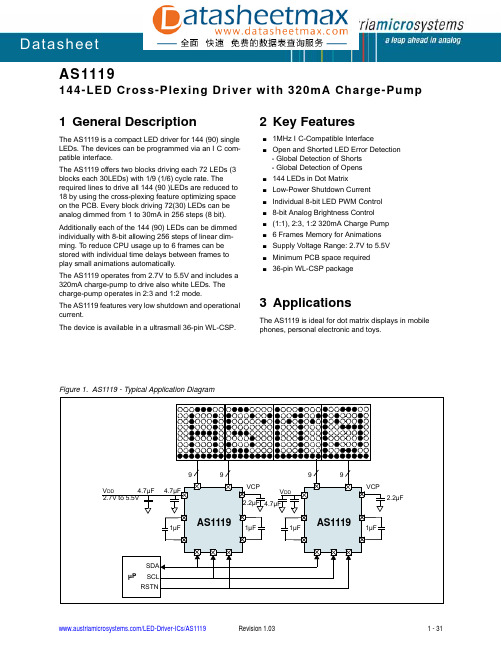
The AS1119 features very low shutdown and operational current.
AS1119
Datasheet - Pinout
电子发烧友 电子技术论坛
Table 1. Pin Descriptions
Pin Name CS0 - CS8
Pin Number
A5-A3, B4-B2, C4-C2
B4
B5
B6
CS6
AD0
SDA
C4
C5
C6
CS9
AD1
SCL
D4
D5
D6
CS12
VDD2
IRQ
E4
E5
E6
CS15 F4
GND2 F5
RSTN F6
Pin Descriptions
Table 1. Pin Descriptions
Pin Name VDD1, VDD2,
VDD3 VCP C1-, C1+ C2-, C2+ GND1 GND2 GND3 SDA SCL AD0 AD1
RSTN
SYNC_IN, SYNC_OUT
IRQ
Pin Number
A6, E5, E1
F1 B1, C1 A1, D1
B5 F5 A2 C6 D6 C5 D5
F6
Description Positive Supply Voltage. Connect to a +2.7V to +5.5V supply. Bypass this pin with 10µF capacitance to GND1, GND2, GND3. Charge-Pump Output Voltage. Connect a 2.2µF capacitor to GND3. Flying Cap 1. Connect a 1µF capacitor. Flying Cap 2. Connect a 1µF capacitor. Ground for VDD1. Used for CS0-CS8 Ground for VDD2. Used for CS9-CS17 Ground for VDD3. Used for Charge-Pump Serial-Data I/O. Open drain digital I/O I²C data pin. Serial-Clock Input. I²C Address for bit 0. Put to GND or VDD to set I²C addresses. I²C Address for bit 1. Put to GND or VDD to set I²C addresses. Reset Input. Pull this pin to logic low to reset all control registers (set to default values) and to put the device into power-down. For normal operation pull this pin to VDD.
IC datasheet pdf-OPA743,OPA2743,OPA4743,pdf(CMOS, Rail-to-Rail, I_O Operational Amplifiers)

ELECTROSTATIC DISCHARGE SENSITIVITY
This integrated circuit can be damaged by ESD. Texas Instruments recommends that all integrated circuits be handled with appropriate precautions. Failure to observe proper handling and installation procedures can cause damage.
OPA2743EA
MSOP-8
337
E43
OPA2743EA/250
Tape and Reel
"
"
"
"
OPA2743EA/2K5
Tape and Reel
OPA2743UA
"
SO-8
"
182
OPA2743UA
OPA2743UA
Rails
"
"
OPA2743UA/2K5
Tape and Reel
OPA2743PA
OPA743
Out 1 V– 2 +In 3
OPA743
5 V+ 4 –In
SOT23-5
Out A 1 –In A 2 +In A 3
V– 4
OPA2743
A B
NC 1 –In 2 +In 3 V– 4
SO-8, DIP-8 8 V+ 7 Out B 6 –In B 5 +In B
8 NC 7 V+ 6 Out 5 NC Out A 1
IC datasheet pdf-PCM3008,pdf(Low Power and Low Voltage 16-Bit, Single-Ended Analog Input_Output Ster
PACKAGE MARKING
ORDERING NUMBER(1)
TRANSPORT MEDIA
PCM3008T TSSOP–16
ZZ363{
–25 °C to +85 °C
PCM3008T
PCM3008T PCM3008T/2K
Rails Tape and Reel
† TI equivalent no. 4040064.
Pop-Noise Free Muting
D Sampling Rate: 8 kHz to 48 kHz D System Clock: 256fS, 384fS, 512fS D Low Voltage Power Supply:
– 2.4 V TYP, 2.1 V MIN to 3.6 V MAX
–
Decimation and
High Pass Filter
Serial Interface
LRCK BCK DIN DOUT
VOUTL VOUTR
Analog Low-Pass
Filter
Analog Low-Pass
Filter
Delta-Sigma Modulator
Interpolation Filter
– Single-Ended Voltage Input – Anti-Aliasing Filter Included – High Performance
– THD+N: –84 dB – SNR: 88 dB – Dynamic Range: 88 dB – 1/64× Decimation Digital Filter – Passband Ripple: ±0.05 dB – Stopband Attenuation: –65 dB – Digital HPF Included
OPA2380 DataSheet
proper handling and installation procedures can cause damage. ESD damage can range from subtle performance degradation to complete device failure. Precision integrated circuits may be more susceptible to damage because very small parametric changes couldPACKAGING INFORMATION Orderable DeviceStatus (1)Package Type Package Drawing Pins Package Qty Eco Plan (2)Lead/Ball Finish MSL Peak Temp (3)OPA2380AIDGKRACTIVE MSOP DGK 82500Green (RoHS &no Sb/Br)CU NIPDAU Level-2-260C-1YEAR OPA2380AIDGKTACTIVE MSOP DGK 8250Green (RoHS &no Sb/Br)CU NIPDAU Level-2-260C-1YEAR OPA380AIDACTIVE SOIC D 8100None CU SNPB Level-1-220C-UNLIM OPA380AIDGKRACTIVE MSOP DGK 82500None CU NIPDAU Level-1-220C-UNLIM OPA380AIDGKTACTIVE MSOP DGK 8250None CU NIPDAU Level-1-220C-UNLIM OPA380AIDRACTIVE SOIC D 82500None CU SNPB Level-1-220C-UNLIM (1)The marketing status values are defined as follows:ACTIVE:Product device recommended for new designs.LIFEBUY:TI has announced that the device will be discontinued,and a lifetime-buy period is in effect.NRND:Not recommended for new designs.Device is in production to support existing customers,but TI does not recommend using this part in a new design.PREVIEW:Device has been announced but is not in production.Samples may or may not be available.OBSOLETE:TI has discontinued the production of the device.(2)Eco Plan -May not be currently available -please check /productcontent for the latest availability information and additional product content details.None:Not yet available Lead (Pb-Free).Pb-Free (RoHS):TI's terms "Lead-Free"or "Pb-Free"mean semiconductor products that are compatible with the current RoHS requirements for all 6substances,including the requirement that lead not exceed 0.1%by weight in homogeneous materials.Where designed to be soldered at high temperatures,TI Pb-Free products are suitable for use in specified lead-free processes.Green (RoHS &no Sb/Br):TI defines "Green"to mean "Pb-Free"and in addition,uses package materials that do not contain halogens,including bromine (Br)or antimony (Sb)above 0.1%of total product weight.(3)MSL,Peak Temp.--The Moisture Sensitivity Level rating according to the JEDECindustry standardclassifications,and peak solder temperature.Important Information and Disclaimer:The information provided on this page represents TI's knowledge and belief as of the date that it is provided.TI bases its knowledge and belief on information provided by third parties,and makes no representation or warranty as to the accuracy of such information.Efforts are underway to better integrate information from third parties.TI has taken and continues to take reasonable steps to provide representative and accurate information but may not have conducted destructive testing or chemical analysis on incoming materials and chemicals.TI and TI suppliers consider certain information to be proprietary,and thus CAS numbers and other limited information may not be available for release.In no event shall TI's liability arising out of such information exceed the total purchase price of the TI part(s)at issue in this document sold by TI to Customer on an annual basis.PACKAGE OPTION ADDENDUM 9-Dec-2004Addendum-Page 1IMPORTANT NOTICETexas Instruments Incorporated and its subsidiaries (TI) reserve the right to make corrections, modifications, enhancements, improvements, and other changes to its products and services at any time and to discontinue any product or service without notice. Customers should obtain the latest relevant information before placing orders and should verify that such information is current and complete. All products are sold subject to TI’s terms and conditions of sale supplied at the time of order acknowledgment.TI warrants performance of its hardware products to the specifications applicable at the time of sale in accordance with TI’s standard warranty. T esting and other quality control techniques are used to the extent TI deems necessary to support this warranty. Except where mandated by government requirements, testing of all parameters of each product is not necessarily performed.TI assumes no liability for applications assistance or customer product design. Customers are responsible for their products and applications using TI components. T o minimize the risks associated with customer products and applications, customers should provide adequate design and operating safeguards.TI does not warrant or represent that any license, either express or implied, is granted under any TI patent right, copyright, mask work right, or other TI intellectual property right relating to any combination, machine, or process in which TI products or services are used. Information published by TI regarding third-party products or services does not constitute a license from TI to use such products or services or a warranty or endorsement thereof. Use of such information may require a license from a third party under the patents or other intellectual property of the third party, or a license from TI under the patents or other intellectual property of TI.Reproduction of information in TI data books or data sheets is permissible only if reproduction is without alteration and is accompanied by all associated warranties, conditions, limitations, and notices. Reproduction of this information with alteration is an unfair and deceptive business practice. TI is not responsible or liable for such altered documentation.Resale of TI products or services with statements different from or beyond the parameters stated by TI for that product or service voids all express and any implied warranties for the associated TI product or service and is an unfair and deceptive business practice. TI is not responsible or liable for any such statements. Following are URLs where you can obtain information on other Texas Instruments products and application solutions:Products ApplicationsAmplifiers Audio /audioData Converters Automotive /automotiveDSP Broadband /broadbandInterface Digital Control /digitalcontrolLogic Military /militaryPower Mgmt Optical Networking /opticalnetwork Microcontrollers Security /securityTelephony /telephonyVideo & Imaging /videoWireless /wirelessMailing Address:Texas InstrumentsPost Office Box 655303 Dallas, Texas 75265Copyright 2004, Texas Instruments Incorporated。
IC datasheet pdf-CD54AC273, CD74AC273,CD54ACT273, CD74ACT273,pdf(Octal D Flip-Flop)
Data sheet acquired from Harris SemiconductorSCHS249BFeatures•Buffered Inputs•Typical Propagation Delay- 6.5ns at V CC = 5V , T A = 25o C, C L = 50pF•Exceeds 2kV ESD Protection MIL-STD-883, Method 3015•SCR-Latchup-Resistant CMOS Process and Circuit Design •Speed of Bipolar FAST™/AS/S with Significantly Reduced Power Consumption •Balanced Propagation Delays•AC Types Feature 1.5V to 5.5V Operation and Balanced Noise Immunity at 30% of the Supply •±24mA Output Drive Current -Fanout to 15 FAST™ ICs-Drives 50Ω Transmission LinesPinoutCD54AC273, CD54ACT273(CDIP)CD74AC273, CD74ACT273(PDIP , SOIC)TOP VIEWDescriptionThe ’AC273and ’ACT273devices are octal D-type flip-flops with reset that utilize advanced CMOS logic rmation at the D input is transferred to the Q output on the positive-going edge of the clock pulse.All eight flip-flops are controlled by a common clock (CP)and a common reset (MR).Resetting is accomplished by a low voltage level independent of the clock.1112131415161718201910987654321MR Q0D0D1Q1Q2D3D2Q3GND V CC D7D6Q6Q7Q5D5D4Q4CPOrdering InformationPART NUMBER TEMPERATURERANGE PACKAGE CD74AC273E0o C to 70o C -40o C to 85o C -55o C to 125o C 20 Ld PDIPCD54AC273F3A -55o C to 125o C 20 Ld CDIP CD74ACT273E0o C to 70o C -40o C to 85o C -55o C to 125o C 20 Ld PDIPCD54ACT273F3A -55o C to 125o C 20 Ld CDIP CD74AC273M0o C to 70o C -40o C to 85o C -55o C to 125o C 20 Ld SOICCD74ACT273M 0o C to 70o C -40o C to 85o C -55o C to 125o C20 Ld SOICNOTES:1.When ordering,use the entire part number.Add the suffix 96to obtain the variant in the tape and reel.2.Wafer and die for this part number is available which meets allelectrical specifications.Please contact your local sales office for ordering information.August 1998 - Revised July 2002CD54AC273, CD74AC273CD54ACT273, CD74ACT273Octal D Flip-Flop with ResetFunctional DiagramTRUTH TABLE INPUTSOUTPUTSRESET (MR)CLOCK CP DATA Dn Qn L X X L H ↑H H H ↑L L HLXQ0H =High level (steady state),L =Low level (steady state),X =Irrel-evant,↑=Transition from Low to High level,Q0=The level of Q before the indicated steady-state input conditions were estab-lished.Q0Q1Q2Q3Q4Q5Q6Q7RESET MRD0D1D2D3D4D5D6D7CLOCKCPDATA INPUTSDATAOUTPUTSAbsolute Maximum Ratings Thermal InformationDC Supply Voltage, V CC. . . . . . . . . . . . . . . . . . . . . . . .-0.5V to 6V DC Input Diode Current, I IKFor V I < -0.5V or V I > V CC + 0.5V. . . . . . . . . . . . . . . . . . . . . .±20mA DC Output Diode Current, I OKFor V O < -0.5V or V O > V CC + 0.5V . . . . . . . . . . . . . . . . . . . .±50mA DC Output Source or Sink Current per Output Pin, I OFor V O > -0.5V or V O < V CC + 0.5V . . . . . . . . . . . . . . . . . . . .±50mA DC V CC or Ground Current, I CC or I GND (Note 3) . . . . . . . . .±100mA Operating ConditionsTemperature Range, T A . . . . . . . . . . . . . . . . . . . . . .-55o C to 125o C Supply Voltage Range, V CC (Note 4)AC T ypes. . . . . . . . . . . . . . . . . . . . . . . . . . . . . . . . . . .1.5V to 5.5V ACT T ypes . . . . . . . . . . . . . . . . . . . . . . . . . . . . . . . . .4.5V to 5.5V DC Input or Output Voltage, V I, V O . . . . . . . . . . . . . . . . .0V to V CC Input Rise and Fall Slew Rate, dt/dvAC T ypes, 1.5V to 3V . . . . . . . . . . . . . . . . . . . . . . . . .50ns (Max) AC T ypes, 3.6V to 5.5V. . . . . . . . . . . . . . . . . . . . . . . .20ns (Max) ACT T ypes, 4.5V to 5.5V. . . . . . . . . . . . . . . . . . . . . . .10ns (Max)Thermal Resistance,θJA(Typical, Note 5)E Package. . . . . . . . . . . . . . . . . . . . . . . . . . . . . . . . . . . . .69o C/W M Package. . . . . . . . . . . . . . . . . . . . . . . . . . . . . . . . . . . . .58o C/W Maximum Junction T emperature (Plastic Package) . . . . . . . . . .150o C Maximum Storage Temperature Range . . . . . . . . . .-65o C to 150o C Maximum Lead Temperature (Soldering 10s). . . . . . . . . . . . .300o CCAUTION:Stresses above those listed in“Absolute Maximum Ratings”may cause permanent damage to the device.This is a stress only rating and operation of the device at these or any other conditions above those indicated in the operational sections of this specification is not implied.NOTES:3.For up to 4 outputs per device, add±25mA for each additional output.4.Unless otherwise specified, all voltages are referenced to ground.5.The package thermal impedance is calculated in accordance with JESD 51.DC Electrical SpecificationsPARAMETER SYMBOLTESTCONDITIONS VCC(V)25o C-40o C TO85o C-55o C TO125o CUNITS V I(V)I O(mA)MIN MAX MIN MAX MIN MAXAC TYPESHigh Level Input Voltage V IH-- 1.5 1.2- 1.2- 1.2-V3 2.1- 2.1- 2.1-V5.5 3.85- 3.85- 3.85-V Low Level Input Voltage V IL-- 1.5-0.3-0.3-0.3V3-0.9-0.9-0.9V5.5- 1.65- 1.65- 1.65V High Level Output Voltage V OH V IH or V IL-0.05 1.5 1.4- 1.4- 1.4-V-0.053 2.9- 2.9- 2.9-V-0.05 4.5 4.4- 4.4- 4.4-V-43 2.58- 2.48- 2.4-V-24 4.5 3.94- 3.8- 3.7-V-75(Note 6, 7)5.5-- 3.85---V-50(Note 6, 7)5.5---- 3.85-VLow Level Output VoltageV OLV IH or V IL0.05 1.5-0.1-0.1-0.1V 0.053-0.1-0.1-0.1V 0.05 4.5-0.1-0.1-0.1V 123-0.36-0.44-0.5V 24 4.5-0.36-0.44-0.5V 75(Note 6, 7) 5.5--- 1.65--V 50(Note 6, 7)5.5----- 1.65V Input Leakage Current I I V CC or GND - 5.5-±0.1-±1-±1µA Quiescent Supply Current MSI I CCV CC or GND5.5-8-80-160µAACT TYPESHigh Level Input Voltage V IH -- 4.5 to 5.52-2-2-V Low Level Input Voltage V IL -- 4.5 to 5.5-0.8-0.8-0.8V High Level Output VoltageV OHV IH or V IL-0.05 4.5 4.4- 4.4- 4.4-V -24 4.5 3.94- 3.8- 3.7-V -75(Note 6, 7) 5.5-- 3.85---V -50(Note 6, 7)5.5---- 3.85-V Low Level Output VoltageV OLV IH or V IL0.05 4.5-0.1-0.1-0.1V 24 4.5-0.36-0.44-0.5V 75(Note 6, 7) 5.5--- 1.65--V 50(Note 6, 7)5.5----- 1.65V Input Leakage Current I I V CC or GND - 5.5-±0.1-±1-±1µA Quiescent Supply Current MSII CC V CC or GND 0 5.5-8-80-160µA Additional Supply Current per Input Pin TTL Inputs High 1 Unit Load ∆I CCV CC -2.1- 4.5 to 5.5- 2.4- 2.8-3mANOTES:6.Test one output at a time for a 1-second maximum duration.Measurement is made by forcing current and measuring voltage to minimize power dissipation.7.Test verifies a minimum 50Ω transmission-line-drive capability at 85o C, 75Ω at 125o C.ACT Input Load TableINPUT UNIT LOADDn 0.5MR 0.57CP1NOTE:Unit load is ∆I CC limit specified in DC Electrical Specifications T able, e.g., 2.4mA max at 25o C.DC Electrical Specifications(Continued)PARAMETERSYMBOL TEST CONDITIONSV CC (V)25o C -40o C TO 85o C -55o C TO 125o C UNITS V I (V)I O (mA)MIN MAX MIN MAX MIN MAXPrerequisite For Switching FunctionPARAMETER SYMBOL V CC (V)-40o C TO 85o C-55o C TO 125o CUNITS MIN MAX MIN MAXAC TYPESData to CP Set-Up Time t SU 1.52-2-ns3.3(Note 9)2-2-ns5(Note 10)2-2-ns Hold Time t H 1.52-2-ns3.32-2-ns52-2-ns Removal Time,MR to CP t REM 1.52-2-ns3.32-2-ns52-2-ns MR Pulse Width t W 1.555-63-ns3.3 6.1-7-ns5 4.4-5-ns CP Pulse Width t W 1.555-63-ns3.3 6.1-7-ns5 4.4-5-ns CP Frequency f MAX 1.59-8-MHz3.381-71-MHz5114-100-MHz ACT TYPESData to CP Set-Up Time t SU5(Note 10)2-2-ns Hold Time t H52-2-ns Removal Time MR to CP t REM52-2-ns MR Pulse Width t W5 4.4-5-ns CP Pulse Width t W5 5.3-6-ns CP Frequency f MAX597-85-MHz Switching Specifications Input t r, t f = 3ns, C L= 50pF (Worst Case)PARAMETER SYMBOL V CC (V)-40o C TO 85o C-55o C TO 125o CUNITS MIN TYP MAX MIN TYP MAXAC TYPESPropagation Delay, CP to Qn t PLH, t PHL 1.5--154--169ns3.3(Note 9)4.9-17.2 4.7-18.9ns5(Note 10)3.5-12.3 3.4-13.5nsPropagation Delay,MR to Qnt PLH , t PHL1.5--154--169ns 3.3 4.9-17.2 4.7-18.9ns 53.5-12.3 3.4-13.5ns Input CapacitanceC I ---10--10pF Power Dissipation Capacitance C PD (Note 11)--45--45-pFACT TYPES Propagation Delay,CP to Qnt PLH , t PHL 5(Note 10)3.5-12.3 3.4-13.5ns Propagation Delay,MR to Qn t PLH , t PHL5 3.5-12.3 3.4-13.5ns Input CapacitanceC I ---10--10pF Power Dissipation Capacitance C PD (Note 11)--45--45-pFNOTES:8.Limits tested 100%.9.3.3V Min is at 3.6V, Max is at 3V.10.5V Min is at 5.5V, Max is at 4.5V.11.C PD is used to determine the dynamic power consumption per flip-flop.AC: P D = C PD V CC 2 f i =∑ (C L V CC 2 f o )ACT:P D =C PD V CC 2f i +∑(C L V CC 2f o )+V CC ∆I CC where f i =input frequency,f o =output frequency,C L =output load capacitance,V CC = supply voltage.FIGURE 1.PROPAGATION DELAY TIMES AND CLOCKPULSE WIDTH FIGURE 2.PREREQUISITE AND PROPAGATION DELAYTIMES FOR MASTER RESETSwitching Specifications Input t r , t f = 3ns, C L = 50pF (Worst Case)(Continued)PARAMETERSYMBOL V CC (V)-40o C TO 85o C-55o C TO 125o CUNITS MIN TYP MAX MIN TYP MAX 90%t f t r V SV S V SV SV St PLHt PHLt W 10%10%CP INPUT LEVEL QMR CPINPUT LEVELV SQV St REMV SV St PLHt WGNDINPUT(Q)FIGURE 3.PREREQUISITE FOR CLOCKDV S V S V SV S V S V St H (H)t SU (L)t H (L)t SU (H)CPOUTPUT LEVELDUT OUTPUTR L (NOTE)OUTPUT LOAD500ΩC L 50pFNOTE:For AC Series Only: When V CC = 1.5V , R L = 1k Ω.FIGURE 4.PROPAGATION DELAY TIMESACACT Input LevelV CC 3V Input Switching Voltage, V S 0.5 V CC 1.5V Output Switching Voltage, V S0.5 V CC0.5 V CCPACKAGING INFORMATIONOrderable Device Status(1)PackageType PackageDrawingPins PackageQtyEco Plan(2)Lead/Ball Finish MSL Peak Temp(3)CD54AC273F3A ACTIVE CDIP J201TBD A42N/A for Pkg Type CD54ACT273F3A ACTIVE CDIP J201TBD A42N/A for Pkg Type CD74AC273E ACTIVE PDIP N2020Pb-Free(RoHS)CU NIPDAU N/A for Pkg TypeCD74AC273EE4ACTIVE PDIP N2020Pb-Free(RoHS)CU NIPDAU N/A for Pkg TypeCD74AC273M ACTIVE SOIC DW2025Green(RoHS&no Sb/Br)CU NIPDAU Level-1-260C-UNLIMCD74AC273M96ACTIVE SOIC DW202000Green(RoHS&no Sb/Br)CU NIPDAU Level-1-260C-UNLIMCD74AC273M96E4ACTIVE SOIC DW202000Green(RoHS&no Sb/Br)CU NIPDAU Level-1-260C-UNLIMCD74AC273M96G4ACTIVE SOIC DW202000Green(RoHS&no Sb/Br)CU NIPDAU Level-1-260C-UNLIMCD74AC273ME4ACTIVE SOIC DW2025Green(RoHS&no Sb/Br)CU NIPDAU Level-1-260C-UNLIMCD74AC273MG4ACTIVE SOIC DW2025Green(RoHS&no Sb/Br)CU NIPDAU Level-1-260C-UNLIMCD74ACT273E ACTIVE PDIP N2020Pb-Free(RoHS)CU NIPDAU N/A for Pkg TypeCD74ACT273EE4ACTIVE PDIP N2020Pb-Free(RoHS)CU NIPDAU N/A for Pkg TypeCD74ACT273M ACTIVE SOIC DW2025Green(RoHS&no Sb/Br)CU NIPDAU Level-1-260C-UNLIMCD74ACT273M96ACTIVE SOIC DW202000Green(RoHS&no Sb/Br)CU NIPDAU Level-1-260C-UNLIMCD74ACT273M96E4ACTIVE SOIC DW202000Green(RoHS&no Sb/Br)CU NIPDAU Level-1-260C-UNLIMCD74ACT273M96G4ACTIVE SOIC DW202000Green(RoHS&no Sb/Br)CU NIPDAU Level-1-260C-UNLIMCD74ACT273ME4ACTIVE SOIC DW2025Green(RoHS&no Sb/Br)CU NIPDAU Level-1-260C-UNLIMCD74ACT273MG4ACTIVE SOIC DW2025Green(RoHS&no Sb/Br)CU NIPDAU Level-1-260C-UNLIMCD74ACT273PW ACTIVE TSSOP PW2070Green(RoHS&no Sb/Br)CU NIPDAU Level-1-260C-UNLIMCD74ACT273PWE4ACTIVE TSSOP PW2070Green(RoHS&no Sb/Br)CU NIPDAU Level-1-260C-UNLIMCD74ACT273PWG4ACTIVE TSSOP PW2070Green(RoHS&no Sb/Br)CU NIPDAU Level-1-260C-UNLIMCD74ACT273PWR ACTIVE TSSOP PW202000Green(RoHS&no Sb/Br)CU NIPDAU Level-1-260C-UNLIMCD74ACT273PWRE4ACTIVE TSSOP PW202000Green(RoHS&no Sb/Br)CU NIPDAU Level-1-260C-UNLIMCD74ACT273PWRG4ACTIVE TSSOP PW202000Green(RoHS&no Sb/Br)CU NIPDAU Level-1-260C-UNLIMCD74ACT273SM96ACTIVE SSOP DB202000Green(RoHS&no Sb/Br)CU NIPDAU Level-1-260C-UNLIMCD74ACT273SM96E4ACTIVE SSOP DB202000Green(RoHS&CU NIPDAU Level-1-260C-UNLIMOrderable Device Status(1)PackageType PackageDrawingPins PackageQtyEco Plan(2)Lead/Ball Finish MSL Peak Temp(3)no Sb/Br)CD74ACT273SM96G4ACTIVE SSOP DB202000Green(RoHS&no Sb/Br)CU NIPDAU Level-1-260C-UNLIM(1)The marketing status values are defined as follows:ACTIVE:Product device recommended for new designs.LIFEBUY:TI has announced that the device will be discontinued,and a lifetime-buy period is in effect.NRND:Not recommended for new designs.Device is in production to support existing customers,but TI does not recommend using this part in a new design.PREVIEW:Device has been announced but is not in production.Samples may or may not be available.OBSOLETE:TI has discontinued the production of the device.(2)Eco Plan-The planned eco-friendly classification:Pb-Free(RoHS),Pb-Free(RoHS Exempt),or Green(RoHS&no Sb/Br)-please check /productcontent for the latest availability information and additional product content details.TBD:The Pb-Free/Green conversion plan has not been defined.Pb-Free(RoHS):TI's terms"Lead-Free"or"Pb-Free"mean semiconductor products that are compatible with the current RoHS requirements for all6substances,including the requirement that lead not exceed0.1%by weight in homogeneous materials.Where designed to be soldered at high temperatures,TI Pb-Free products are suitable for use in specified lead-free processes.Pb-Free(RoHS Exempt):This component has a RoHS exemption for either1)lead-based flip-chip solder bumps used between the die and package,or2)lead-based die adhesive used between the die and leadframe.The component is otherwise considered Pb-Free(RoHS compatible)as defined above.Green(RoHS&no Sb/Br):TI defines"Green"to mean Pb-Free(RoHS compatible),and free of Bromine(Br)and Antimony(Sb)based flame retardants(Br or Sb do not exceed0.1%by weight in homogeneous material)(3)MSL,Peak Temp.--The Moisture Sensitivity Level rating according to the JEDEC industry standard classifications,and peak solder temperature.Important Information and Disclaimer:The information provided on this page represents TI's knowledge and belief as of the date that it is provided.TI bases its knowledge and belief on information provided by third parties,and makes no representation or warranty as to the accuracy of such information.Efforts are underway to better integrate information from third parties.TI has taken and continues to take reasonable steps to provide representative and accurate information but may not have conducted destructive testing or chemical analysis on incoming materials and chemicals.TI and TI suppliers consider certain information to be proprietary,and thus CAS numbers and other limited information may not be available for release.In no event shall TI's liability arising out of such information exceed the total purchase price of the TI part(s)at issue in this document sold by TI to Customer on an annual basis.TAPE AND REELINFORMATION*All dimensionsare nominalDevicePackage Type Package Drawing Pins SPQReel Diameter (mm)Reel Width W1(mm)A0(mm)B0(mm)K0(mm)P1(mm)W (mm)Pin1Quadrant CD74AC273M96SOIC DW 202000330.024.410.813.0 2.712.024.0Q1CD74ACT273M96SOIC DW 202000330.024.410.813.0 2.712.024.0Q1CD74ACT273PWR TSSOP PW 202000330.016.4 6.957.1 1.68.016.0Q1CD74ACT273SM96SSOPDB202000330.016.48.27.52.512.016.0Q1PACKAGE MATERIALS INFORMATION11-Mar-2008*Alldimensions are nominal DevicePackage Type Package Drawing Pins SPQ Length (mm)Width (mm)Height (mm)CD74AC273M96SOIC DW 202000346.0346.041.0CD74ACT273M96SOIC DW 202000346.0346.041.0CD74ACT273PWRTSSOP PW 202000346.0346.033.0CD74ACT273SM96SSOP DB 202000346.0346.033.0PACKAGE MATERIALS INFORMATION 11-Mar-2008Pack Materials-Page 2IMPORTANT NOTICETexas Instruments Incorporated and its subsidiaries(TI)reserve the right to make corrections,modifications,enhancements,improvements, and other changes to its products and services at any time and to discontinue any product or service without notice.Customers should obtain the latest relevant information before placing orders and should verify that such information is current and complete.All products are sold subject to TI’s terms and conditions of sale supplied at the time of order acknowledgment.TI warrants performance of its hardware products to the specifications applicable at the time of sale in accordance with TI’s standard warranty.Testing and other quality control techniques are used to the extent TI deems necessary to support this warranty.Except where mandated by government requirements,testing of all parameters of each product is not necessarily performed.TI assumes no liability for applications assistance or customer product design.Customers are responsible for their products and applications using TI components.To minimize the risks associated with customer products and applications,customers should provide adequate design and operating safeguards.TI does not warrant or represent that any license,either express or implied,is granted under any TI patent right,copyright,mask work right, or other TI intellectual property right relating to any combination,machine,or process in which TI products or services are rmation published by TI regarding third-party products or services does not constitute a license from TI to use such products or services or a warranty or endorsement e of such information may require a license from a third party under the patents or other intellectual property of the third party,or a license from TI under the patents or other intellectual property of TI.Reproduction of TI information in TI data books or data sheets is permissible only if reproduction is without alteration and is accompanied by all associated warranties,conditions,limitations,and notices.Reproduction of this information with alteration is an unfair and deceptive business practice.TI is not responsible or liable for such altered rmation of third parties may be subject to additional restrictions.Resale of TI products or services with statements different from or beyond the parameters stated by TI for that product or service voids all express and any implied warranties for the associated TI product or service and is an unfair and deceptive business practice.TI is not responsible or liable for any such statements.TI products are not authorized for use in safety-critical applications(such as life support)where a failure of the TI product would reasonably be expected to cause severe personal injury or death,unless officers of the parties have executed an agreement specifically governing such use.Buyers represent that they have all necessary expertise in the safety and regulatory ramifications of their applications,and acknowledge and agree that they are solely responsible for all legal,regulatory and safety-related requirements concerning their products and any use of TI products in such safety-critical applications,notwithstanding any applications-related information or support that may be provided by TI.Further,Buyers must fully indemnify TI and its representatives against any damages arising out of the use of TI products in such safety-critical applications.TI products are neither designed nor intended for use in military/aerospace applications or environments unless the TI products are specifically designated by TI as military-grade or"enhanced plastic."Only products designated by TI as military-grade meet military specifications.Buyers acknowledge and agree that any such use of TI products which TI has not designated as military-grade is solely at the Buyer's risk,and that they are solely responsible for compliance with all legal and regulatory requirements in connection with such use. TI products are neither designed nor intended for use in automotive applications or environments unless the specific TI products are designated by TI as compliant with ISO/TS16949requirements.Buyers acknowledge and agree that,if they use any non-designated products in automotive applications,TI will not be responsible for any failure to meet such requirements.Following are URLs where you can obtain information on other Texas Instruments products and application solutions:Products ApplicationsAmplifiers AudioData Converters AutomotiveDLP®Products BroadbandDSP Digital ControlClocks and Timers MedicalInterface MilitaryLogic Optical NetworkingPower Mgmt SecurityMicrocontrollers TelephonyRFID Video&ImagingRF/IF and ZigBee®Solutions WirelessMailing Address:Texas Instruments,Post Office Box655303,Dallas,Texas75265Copyright©2009,Texas Instruments Incorporated。
IC datasheet pdf-CAT3606 pdf,datasheet
CAT36066-Channel Low Noise Charge Pump White LED DriverDescriptionThe CAT3606 controls up to four LEDs for the main display and two LEDs for the sub-display in cellular phones. The device is capable of operating in either 1x (LDO) mode or 1.5x charge pump mode. All LED pin currents are regulated and tightly matched to achieve uniformity of brightness across the LCD backlight. An external resistor (R SET) sets the nominal output current.The device can deliver as much as 20 mA per channel during low voltage operation (3 V), and 30 mA per channel during nominal operation (3.3 V). A constant high-frequency switching scheme (1MHz) provides low noise and allows the use of very small value ceramic capacitors.A “zero” quiescent current mode can be achieved via the chip enable pin EN. The Main and Sub LEDs each have their own dedicated ON/OFF control pins ENM, ENS. Dimming can be achieved using either a DC voltage to control the R SET pin current, or by applying a PWM signal on the ENM and ENS pins.The device is available in a 16−pad TQFN package with a max height of 0.8 mm.Features•Drives up to 4 Main LEDs and 2 Sub LEDs•Separate Control for Main and Sub LEDs •Compatible with Supply V oltage of 3 V to 5.5 V•Power Efficiency up to 90%•Output Current up to 30 mA per LED•High−frequency Operation at 1 MHz•2 Modes of Operation 1x and 1.5x•White LED Detect Circuitry on All Channels •Shutdown Current less than 1 m A•Small Ceramic Capacitors•Soft Start and Current Limiting•Short Circuit Protection•16−pad TQFN Package, 0.8 mm Max Height•These Devices are Pb−Free, Halogen Free/BFR Free and are RoHS CompliantApplications•Cell Phone Main and Sub−display Backlight•Navigation •PDAs •Digital CamerasTQFN−16HV4 SUFFIXCASE 510AEPIN CONNECTIONS (Note 1)G366MARKING DIAGRAMSDevice Package ShippingORDERING INFORMATIONCAT3606HV4−T2TQFN−16(Note 2)2,000/Tape & ReelG366 = CAT3606HV4−T2CDBB = CAT3606HV4−GT21.The “exposed pad” under the package must beconnected to the ground plane on the PCB.2.Matte−Tin Plated Finish (RoHS−compliant).3.NiPdAu Plated Finish (RoHS−compliant).LED5LED4LED3LED2LED1C2+C2−C1−LED6ENENMENSRSETVOUTVINC1+1(4 x 4 mm) (Top View)CDBBCAT3606HV4−GT2TQFN−16(Note 3)GNDFigure 1. Typical Application Circuitm FLi −OUT Table 1. PIN DESCRIPTIONPin #Name Function1LED6LED6 cathode terminal2EN Enable/shutdown input, active high3ENM Enable “main” input for LED1 to LED4, active low 4ENS Enable “sub” input for LED5 and LED6, active low5RSET The LED output current is set by the current sourced out of the RSET pin 6VOUT Charge pump output connected to the LED anodes 7VIN Supply voltage8C1+Bucket capacitor 1 terminal 9C1Bucket capacitor 1 terminal 10C2Bucket capacitor 2 terminal 11C2+Bucket capacitor 2 terminal 12LED1LED 1 cathode terminal 13LED2LED 2 cathode terminal 14LED3LED 3 cathode terminal 15LED4LED 4 cathode terminal 16LED5LED 5 cathode terminal PADGNDGround referenceTable 2. ABSOLUTE MAXIMUM RATINGSParameter Rating Unit VIN, VOUT, LEDx voltage−0.3 to 7.0V EN, ENM, ENS voltage−0.3 to VIN V RSET voltage−0.3 to VIN V RSET current±1mA Ambient Temperature Range−40 to +85_C Storage Temperature Range−65 to +160_C Lead Temperature300_C ESD Rating HBM (Human Body Model)2,000V ESD Rating MM (Machine Model) (Note 4)200V Stresses exceeding Maximum Ratings may damage the device. Maximum Ratings are stress ratings only. Functional operation above the Recommended Operating Conditions is not implied. Extended exposure to stresses above the Recommended Operating Conditions may affect device reliability.4.Machine model is with 200 pF capacitor discharged directly into each pin.Table 3. RECOMMENDED OPERATING CONDITIONSParameter Range Unit VIN 3.0 to 5.5V Ambient Temperature Range−40 to +85_C Input/Output/Bucket Capacitors 1 ±20% Typical m FI LED per LED pin0 to 30mAI OUT Total Output Current0 to 150mA Table 4. ELECTRICAL OPERATING CHARACTERISTICS(Limits over recommended operating conditions unless specified otherwise. Typical values at T A = 25°C, V IN = 3.5 V, I RSET = 5 m A.) Symbol Parameter Conditions Min Typ Max UnitI Q Quiescent Current V EN= 0 V1x Mode, No Load1.5x Mode, No Load 0.10.32.6115m AmAmAV RSET RSET Regulated Voltage 1.17 1.2 1.23VI LED Programmed LED Current I RSET = 5 m AI RSET = 37 m AI RSET = 78 m A 2.415.030.0mAI LED LED Current Range with 6 LEDs 3.3 ≤ VIN ≤ 4.5 V3.0 ≤ VIN ≤4.5 V 3020mAI LED LED Current Range with 4 LEDs 3.3 ≤ VIN ≤ 4.5 V30mAI LED−ACC LED Current Accuracy0.5 mA ≤ I LED≤ 3 mA3 mA ≤ I LED≤ 30 mA ±15±5%I LED−DEV LED Channel Matching(I LED – I LEDAVG) / I LEDAVG±3%R OUT Output Resistance(Open Loop)1x Mode,1.5x Mode, I OUT = 100 mA1.46.52.510Wf OSC Charge Pump Frequency0.8 1.0 1.3MHz T DROPOUT1x to 1.5x Mode Transition Dropout Delay0.40.60.9ms I EN−CTR Input Leakage Current On Inputs EN, ENM, ENS1m AV EN−CTR High Detect ThresholdLow Detect Threshold On Inputs EN, ENM, ENS0.40.80.71.3VI SC Input Current Limit VOUT = GND304560mA I LIM Maximum Input Current VOUT > 1 V200400600mABlock DiagramFigure 2. CAT3606 Functional Block Diagramm FVBasic OperationAt power-up, the CA T3606 starts operation in 1x mode. If it is able to drive the programmed LED current, it continues in 1x mode. If the battery voltage drops to a level where the LED current cannot be met, the driver automatically switches into 1.5x mode, to boost the output voltage high enough to achieve the nominal LED current.The above sequence is reinitialized each and every time the chip is powered up or is taken out of shutdown mode (via EN pin). The use of the Main and Sub display enable pins (ENM or ENS) does not affect the mode of operation. LED Current SettingThe LED current is set by the external resistor R SET connected between the RSET pin and ground. Table 5 lists various LED currents and the associated R SET resistor value for standard 1% precision surface mount resistors.Table 5. RSET Resistor SelectionLED Current (mA)R SET (k W)1649228751021049.91532.42023.73015.4The enable lines ENM and ENS allow to turn On or Off a group of LEDs as shown in Table 6.Table 6. LED SelectionControl Lines LED Outputs EN ENM ENSMainLED1 − LED4SubLED5 −LED6 0X X––111––101ON−110−ON100ON ON NOTES:1 = logic high (or VIN)0 = logic low (or GND)– = LED output OFFX = don’t careThe unused LED channels can also be turned off by connecting the respective LED pins to VOUT. In which case, the corresponding LED driver is disabled and the typical LED sink current is only about 0.2 mA. When the following equation is true on any channel, the driver turns off the LED channel:VOUT*V LED v1V(LED channel OFF) Note: The CA T3606 is designed to drive LEDs with forward voltage greater than 1 V and is not compatible with resistive loads.Figure 3. Efficiency vs. Input Voltage(6 LEDs)Figure 4. Efficiency vs. Total LED Current(6 LEDs)INPUT VOLTAGE (V)TOTAL LED CURRENT (mA)405060708090100405060708090100Figure 5. LED Current vs. Input VoltageFigure 6. LED Current Change vs.TemperatureINPUT VOLTAGE (V)TEMPERATURE (°C)−−−0.51.5−−Figure 7. Ground Current vs. Input Voltage(1x Mode)Figure 8. Ground Current vs. Temperature(1x Mode)INPUT VOLTAGE (V)TEMPERATURE (°C)0.10.20.30.40.500.10.20.30.40.5E F F I C I E N C Y (%)E F F I C I E N C Y (%)L E D C U R R E N T C H A N G E (%)L E D C U R R E N T C H A N G E (%)G R O U N D C U R R E N T (m A )G R O U N D C U R R E N T (m A )01.0−−Figure 9. Ground Current vs. Input Voltage(1.5x Mode)Figure 10. Supply Current vs. Input VoltageINPUT VOLTAGE (V)INPUT VOLTAGE (V)134580120140Figure 11. Oscillator Frequency vs. InputVoltageFigure 12. Oscillator Frequency vs.TemperatureINPUT VOLTAGE (V)TEMPERATURE (°C)0.900.951.001.051.100.900.951.001.051.10Figure 13. Output Resistance vs. Input Voltage(1x Mode)Figure 14. Output Resistance vs. Input Voltage(1.5x Mode)INPUT VOLTAGE (V)INPUT VOLTAGE (V)1234246810G R O U N D C U R R E N T (m A )G R O U N D C U R R E N T (m A )C L O C K F R E Q U E N C Y (M H z )C L O C K F R E Q U E N C Y (M H z )O U T P U T R E S I S T A N C E (W )O U T P U T R E S I S T A N C E (W )2100Figure 15. Switching Waveforms in 1.5x Mode Figure 16. Operating Waveforms in 1x Mode400 nsec/div400 nsec/divCurrent Input 50mV/VIN 50mV/divVOUT Input 50mV/div VIN Figure 17. Power Up 6 LEDs at 15 mA,VIN = 3 V (1.5x Mode)Figure 18. Power Up 6 LEDs at 15 mA,VIN = 3.6 V (1x Mode)400 m sec/div400 m sec/div2V/divVOUT 2V/div EN 2V/divVOUT 100mA/divInput 2V/divEN Figure 19. LED Current vs. R SETFigure 20. Line Transient Responsein 1x ModeRSET (k W )200 m sec/div10,000100100.1101002V/div VOUT 5mA/div Input 1V/div3.6V to4.9VVinL E D C U R R E N T (m A )10mA/Input Current 100mA/divAC coupledCurrent 10mA/div AC coupledAC coupledVOUT 50mV/divdiv divCurrent Current 10001(V IN = 3.6 V, EN = V IN , ENM = ENS = GND, C IN = C OUT = 1 m F, T AMB = 25°C, unless otherwise specified.)Figure 21. Foldback Current Limiting OUTPUT CURRENT (mA)5004003002001000012345O U TP U T V O L T A G E (V )1x ModeFigure 22. RSET Pin Voltage vs. Temperature−50−2502550751001251.161.181.201.221.24R S E T P I N V O L T A G E (V )Figure 23. PWM Dimming at 1 kHz on ENM and ENS50mA/divCurrent Tot. LED 1V/divVOUT ENM & ENS5V/div200 m sec/divTEMPERATURE (°C)Recommended LayoutWhen the driver is in the 1.5x charge pump mode, the 1MHz switching frequency operation requires to minimize trace length and impedance to ground on all 4 capacitors. A ground plane should cover the area on the bottom side of the PCB opposite to the IC and the bypass capacitors.Capacitors Cin and Cout require short connection to ground which can be done with multiple vias as shown on Figure 24.A square copper area matches the QFN16 exposed pad (GND) and must be connected to the ground plane underneath. The use of multiple via will improve the heat dissipation.Figure 24. PCB LayoutPACKAGE DIMENSIONSTQFN16, 4x4CASE 510AE−01ISSUE AA3A1SIDE VIEWTOP VIEW BOTTOM VIEWDETAIL AFRONT VIEWNotes:(1) All dimensions are in millimeters.(2) Complies with JEDEC MO-220.SYMBOL MIN NOM MAXA0.700.750.80A10.000.020.05A30.20 REFb0.250.300.35D 3.90 4.00 4.10D2 2.00−−− 2.25E 4.00E2 2.00−−− 2.25e3.900.65 BSC4.10L0.45−−−0.65CAT3606Example of Ordering Information (Note 7)PrefixDevice #Suffix 5.All packages are RoHS −compliant (Lead −free, Halogen −free).6.The standard lead finish is NiPdAu.7.The device used in the above example is a CAT3606HV4−GT2 (TQFN, NiPdAu Plated Finish, Tape & Reel, 2,000/Reel).8.For Matte −Tin package option, please contact your nearest ON Semiconductor Sales office.9.For information on tape and reel specifications, including part orientation and tape sizes, please refer to our Tape and Reel Packaging Specifications Brochure, BRD8011/D.ON Semiconductor and are registered trademarks of Semiconductor Components Industries, LLC (SCILLC). SCILLC reserves the right to make changes without further notice to any products herein. SCILLC makes no warranty, representation or guarantee regarding the suitability of its products for any particular purpose, nor does SCILLC assume any liability arising out of the application or use of any product or circuit, and specifically disclaims any and all liability, including without limitation special, consequential or incidental damages.“Typical” parameters which may be provided in SCILLC data sheets and/or specifications can and do vary in different applications and actual performance may vary over time. All operating parameters, including “Typicals” must be validated for each customer application by customer’s technical experts. SCILLC does not convey any license under its patent rights nor the rights of others. SCILLC products are not designed, intended, or authorized for use as components in systems intended for surgical implant into the body, or other applications intended to support or sustain life, or for any other application in which the failure of the SCILLC product could create a situation where personal injury or death may occur. Should Buyer purchase or use SCILLC products for any such unintended or unauthorized application, Buyer shall indemnify and hold SCILLC and its officers, employees, subsidiaries, affiliates,and distributors harmless against all claims, costs, damages, and expenses, and reasonable attorney fees arising out of, directly or indirectly, any claim of personal injury or death associated with such unintended or unauthorized use, even if such claim alleges that SCILLC was negligent regarding the design or manufacture of the part. SCILLC is an Equal Opportunity/Affirmative Action Employer. This literature is subject to all applicable copyright laws and is not for resale in any manner.PUBLICATION ORDERING INFORMATION。
OPA2333A-EP资料
PRODUCT OPA333AMDBVREP OPA333AMDCKREP OPA2333AMDREP
ORDERING INFORMATION(1)
PACKAGE-LEAD SOT23-5 SC70-5 SO-8
PACKAGE DESIGNATOR DBV DCK D
PACKAGE MARKING(2) OBYM CHQ 2333EP
(2) Input terminals are diode clamped to the power-supply rails. Input signals that can swing more than 0.3 V beyond the supply rails should be current limited to 10 mA or less.
Absolute Maximum Ratings(1)
over operating free-air temperature range (unless otherwise noted)
Supply voltage Signal input terminals, voltage(2) Output short circuit(3) Operating temperature range Storage temperature range Junction temperature
IC datasheet pdf-NCP5603 pdf,datasheet
Rating Power Supply Voltage Power Supply Current Digital Input Pins Digital Input Pins Output Voltage ESD Capability (Note 3) Human Body Model Machine Model DFN10, 3x3 Package Power Dissipation @ Tamb = +85°C Thermal Resistance, Junction-to-Air (RqJA) Operating Ambient Temperature Range Operating Junction Temperature Range Maximum Junction Temperature Storage Temperature Range Latchup Current Maximum Rating Moisture Sensitivity Level (MSL) Symbol Vbat Ibat Vin Iin Vout VESD 2.5 200 PDS RqJA TA TJ TJmax Tstg 580 68.5 -40 to +85 -40 to +125 +150 -65 to +150 100 mA per JEDEC standard, JESD78 1 per IPC/JEDEC standard, J-STD-020A kV V mW °C/W °C °C °C °C Value 7.0 800 -0.5 V < Vbat < Vbat +0.5 V < 6.0 V "5.0 5.5 Unit V mA V mA V
- 1、下载文档前请自行甄别文档内容的完整性,平台不提供额外的编辑、内容补充、找答案等附加服务。
- 2、"仅部分预览"的文档,不可在线预览部分如存在完整性等问题,可反馈申请退款(可完整预览的文档不适用该条件!)。
- 3、如文档侵犯您的权益,请联系客服反馈,我们会尽快为您处理(人工客服工作时间:9:00-18:30)。
2
Submit Documentation Feedback
Copyright © 2008–2010, Texas Instruments Incorporated Product Folder Link(s): OPA2333-Q1
OPA2333-Q1
PARAMETER
TEST CONDITIONS
MIN
TYP
MAX UNIT
OFFSET VOLTAGE
Input offset voltage over temperature
VOS
VS = 5 V
2
10 mV
22 mV
vs temperature vs power supply Long-term stability(1)
PRODUCTION DATA information is current as of publication date. Products conform to specifications per the terms of the Texas Instruments standard warranty. Production processing does not necessarily include testing of all parameters.
in
INPUT VOLTAGE RANGE
100
fA/√Hz
Common mode voltage range
Common-Mode Rejection Ratio
VCM CMRR
(V–) – 0.1 V < VCM < (V+) + 0.1 V
(V–) – 0.1 102
(V+) + 0.1
V
130
dB
INPUT CAPACITANCE
Differential
2
pF
Common mode
4
pF
OPEN-LOOP GAIN
Open-loop voltage gain
AOL
(V–) + 100 mV < VO < (V+) – 100 mV, RL = 10 kΩ
104
130
dB
FREQUENCY RESPONSE
dVOS/dT PSRR
VS = 1.8 V to 5.5 V
0.02 1
(1)
mV/°C 6 mV/V
Channel separation, dc
0.1
mV/V
INPUT BIAS CURRENT
Input bias current
IB
over Temperature
±70 ±150
±200
pA
pA
Copyright © 2008–2010, Texas Instruments Incorporated
OPA2333-Q1
SBOS463A – DECEMBER 2008 – REVISED JUNE 2010
ABSOLUTE MAXIMUM RATINGS(1)
over operating free-air temperature range (unless otherwise noted)
1s/div
DESCRIPTION/ORDERING INFORMATION
The OPA2333A CMOS operational amplifiers use a proprietary auto-calibration technique to simultaneously provide very low offset voltage (10 mV max) and near-zero drift over time and temperature. These miniature high-precision low-quiescent-current amplifiers offer high-impedance inputs that have a common-mode range 100 mV beyond the rails and rail-to-rail output that swings within 50 mV of the rails. Single or dual supplies as low as 1.8 V (±0.9 V) and up to 5.5 V (±2.75 V) may be used. They are optimized for low-voltage single-supply operation.
(2) Package drawings, thermal data, and symbolization are available at /packaging.
1
Please be aware that an important notice concerning availability, standard warranty, and use in critical applications of Texas Instruments semiconductor products and disclaimers thereto appears at the end of this data sheet.
Gain-bandwidth product Slew rate
GBW SR
CL = 100 pF G=1
350
kHz
0.16
V/ms
(1) 300-hour life test at 150°C demonstrated randomly distributed variation of approximately 1 mV.
FEATURES
1
• Qualified for Automotive Applications • Low Offset Voltage: 23 mV (Max) • 0.01-Hz to 10-Hz Noise: 1.1 mVPP • Quiescent Current: 17 mA • Single-Supply Operation • Supply Voltage: 1.8 V to 5.5 V • Rail-to-Rail Input/Output
The OPA2333A is specified for operation from –40°C to 125°C.
TA –40°C to 125°C
SOIC – D MSOP – DGK
ORDERING INFORMATION(1)
PACKAGE (2)
ORDERABLE PART NUMBER
(2) Input terminals are diode clamped to the power-supply rails. Input signals that can swing more than 0.3 V beyond the supply rails should be current limited to 10 mA or less.
2000 V 1000 V
(1) Stresses beyond those listed under absolute maximum ratings may cause permanent damage to the device. These are stress ratings only, and functional operation of the device at these or any other conditions beyond those indicated under recommended operating conditions is not implied. Exposure to absolute-maximum-rated conditions for extended periods may affect device reliability.
OPA2333-Q1
SBOS463A – DECEMBER 2008 – REVISED JUNE 2010
1.8-V MICROPOWER CMOS OPERATIONAL AMPLIFIER ZERO-DRIFT SERIES
Check for Samples: OPA2333-Q1
Reel of 2500
OPA2333AQDRQ1
Reel of 2500
OPA2333AQDGKRQ1
TOP-SIDE MARKING 02333Q OCOQ
(1) For the most current package and ordering information, see the Package Option Addendum at the end of this document, or see the TI web site at .
Input offset current
IOS
NOISE
±140
±400
pA
Input voltage noise, f = 0.01 Hz to 1 Hz
0.3
mVPP
Input voltage noise, f = 0.1 Hz to 10 Hz
1.1
mVPP
Input current noise, f = 10 Hz
VCC VI IO(SS) TA TJ Tstg
Supply voltage Input voltage, signal input terminals(2) Output short-circuit circuit(3) Operating free-air temperature range Maximum operating virtual-junction temperature Storage temperature range